JP4265796B2 - 受熱シート、電子機器及び受熱シートの製造方法 - Google Patents
受熱シート、電子機器及び受熱シートの製造方法 Download PDFInfo
- Publication number
- JP4265796B2 JP4265796B2 JP2005084794A JP2005084794A JP4265796B2 JP 4265796 B2 JP4265796 B2 JP 4265796B2 JP 2005084794 A JP2005084794 A JP 2005084794A JP 2005084794 A JP2005084794 A JP 2005084794A JP 4265796 B2 JP4265796 B2 JP 4265796B2
- Authority
- JP
- Japan
- Prior art keywords
- heat
- receiving sheet
- sheet
- silicone rubber
- base material
- Prior art date
- Legal status (The legal status is an assumption and is not a legal conclusion. Google has not performed a legal analysis and makes no representation as to the accuracy of the status listed.)
- Expired - Fee Related
Links
Images

Classifications
-
- H—ELECTRICITY
- H05—ELECTRIC TECHNIQUES NOT OTHERWISE PROVIDED FOR
- H05K—PRINTED CIRCUITS; CASINGS OR CONSTRUCTIONAL DETAILS OF ELECTRIC APPARATUS; MANUFACTURE OF ASSEMBLAGES OF ELECTRICAL COMPONENTS
- H05K7/00—Constructional details common to different types of electric apparatus
- H05K7/20—Modifications to facilitate cooling, ventilating, or heating
- H05K7/2039—Modifications to facilitate cooling, ventilating, or heating characterised by the heat transfer by conduction from the heat generating element to a dissipating body
- H05K7/20518—Unevenly distributed heat load, e.g. different sectors at different temperatures, localised cooling, hot spots
-
- B—PERFORMING OPERATIONS; TRANSPORTING
- B32—LAYERED PRODUCTS
- B32B—LAYERED PRODUCTS, i.e. PRODUCTS BUILT-UP OF STRATA OF FLAT OR NON-FLAT, e.g. CELLULAR OR HONEYCOMB, FORM
- B32B3/00—Layered products comprising a layer with external or internal discontinuities or unevennesses, or a layer of non-planar shape; Layered products comprising a layer having particular features of form
- B32B3/10—Layered products comprising a layer with external or internal discontinuities or unevennesses, or a layer of non-planar shape; Layered products comprising a layer having particular features of form characterised by a discontinuous layer, i.e. formed of separate pieces of material
- B32B3/18—Layered products comprising a layer with external or internal discontinuities or unevennesses, or a layer of non-planar shape; Layered products comprising a layer having particular features of form characterised by a discontinuous layer, i.e. formed of separate pieces of material characterised by an internal layer formed of separate pieces of material which are juxtaposed side-by-side
- B32B3/20—Layered products comprising a layer with external or internal discontinuities or unevennesses, or a layer of non-planar shape; Layered products comprising a layer having particular features of form characterised by a discontinuous layer, i.e. formed of separate pieces of material characterised by an internal layer formed of separate pieces of material which are juxtaposed side-by-side of hollow pieces, e.g. tubes; of pieces with channels or cavities
-
- B—PERFORMING OPERATIONS; TRANSPORTING
- B32—LAYERED PRODUCTS
- B32B—LAYERED PRODUCTS, i.e. PRODUCTS BUILT-UP OF STRATA OF FLAT OR NON-FLAT, e.g. CELLULAR OR HONEYCOMB, FORM
- B32B7/00—Layered products characterised by the relation between layers; Layered products characterised by the relative orientation of features between layers, or by the relative values of a measurable parameter between layers, i.e. products comprising layers having different physical, chemical or physicochemical properties; Layered products characterised by the interconnection of layers
- B32B7/02—Physical, chemical or physicochemical properties
- B32B7/027—Thermal properties
-
- G—PHYSICS
- G06—COMPUTING OR CALCULATING; COUNTING
- G06F—ELECTRIC DIGITAL DATA PROCESSING
- G06F1/00—Details not covered by groups G06F3/00 - G06F13/00 and G06F21/00
- G06F1/16—Constructional details or arrangements
- G06F1/20—Cooling means
-
- H—ELECTRICITY
- H05—ELECTRIC TECHNIQUES NOT OTHERWISE PROVIDED FOR
- H05K—PRINTED CIRCUITS; CASINGS OR CONSTRUCTIONAL DETAILS OF ELECTRIC APPARATUS; MANUFACTURE OF ASSEMBLAGES OF ELECTRICAL COMPONENTS
- H05K7/00—Constructional details common to different types of electric apparatus
- H05K7/20—Modifications to facilitate cooling, ventilating, or heating
- H05K7/2039—Modifications to facilitate cooling, ventilating, or heating characterised by the heat transfer by conduction from the heat generating element to a dissipating body
- H05K7/20436—Inner thermal coupling elements in heat dissipating housings, e.g. protrusions or depressions integrally formed in the housing
- H05K7/20445—Inner thermal coupling elements in heat dissipating housings, e.g. protrusions or depressions integrally formed in the housing the coupling element being an additional piece, e.g. thermal standoff
- H05K7/20463—Filling compound, e.g. potted resin
-
- H—ELECTRICITY
- H10—SEMICONDUCTOR DEVICES; ELECTRIC SOLID-STATE DEVICES NOT OTHERWISE PROVIDED FOR
- H10W—GENERIC PACKAGES, INTERCONNECTIONS, CONNECTORS OR OTHER CONSTRUCTIONAL DETAILS OF DEVICES COVERED BY CLASS H10
- H10W40/00—Arrangements for thermal protection or thermal control
-
- H—ELECTRICITY
- H10—SEMICONDUCTOR DEVICES; ELECTRIC SOLID-STATE DEVICES NOT OTHERWISE PROVIDED FOR
- H10W—GENERIC PACKAGES, INTERCONNECTIONS, CONNECTORS OR OTHER CONSTRUCTIONAL DETAILS OF DEVICES COVERED BY CLASS H10
- H10W40/00—Arrangements for thermal protection or thermal control
- H10W40/20—Arrangements for cooling
- H10W40/25—Arrangements for cooling characterised by their materials
- H10W40/251—Organics
-
- H—ELECTRICITY
- H10—SEMICONDUCTOR DEVICES; ELECTRIC SOLID-STATE DEVICES NOT OTHERWISE PROVIDED FOR
- H10W—GENERIC PACKAGES, INTERCONNECTIONS, CONNECTORS OR OTHER CONSTRUCTIONAL DETAILS OF DEVICES COVERED BY CLASS H10
- H10W40/00—Arrangements for thermal protection or thermal control
- H10W40/20—Arrangements for cooling
- H10W40/25—Arrangements for cooling characterised by their materials
- H10W40/257—Arrangements for cooling characterised by their materials having a heterogeneous or anisotropic structure, e.g. powder or fibres in a matrix, wire mesh or porous structures
-
- Y—GENERAL TAGGING OF NEW TECHNOLOGICAL DEVELOPMENTS; GENERAL TAGGING OF CROSS-SECTIONAL TECHNOLOGIES SPANNING OVER SEVERAL SECTIONS OF THE IPC; TECHNICAL SUBJECTS COVERED BY FORMER USPC CROSS-REFERENCE ART COLLECTIONS [XRACs] AND DIGESTS
- Y10—TECHNICAL SUBJECTS COVERED BY FORMER USPC
- Y10T—TECHNICAL SUBJECTS COVERED BY FORMER US CLASSIFICATION
- Y10T428/00—Stock material or miscellaneous articles
- Y10T428/24—Structurally defined web or sheet [e.g., overall dimension, etc.]
- Y10T428/24802—Discontinuous or differential coating, impregnation or bond [e.g., artwork, printing, retouched photograph, etc.]
- Y10T428/24843—Discontinuous or differential coating, impregnation or bond [e.g., artwork, printing, retouched photograph, etc.] with heat sealable or heat releasable adhesive layer
-
- Y—GENERAL TAGGING OF NEW TECHNOLOGICAL DEVELOPMENTS; GENERAL TAGGING OF CROSS-SECTIONAL TECHNOLOGIES SPANNING OVER SEVERAL SECTIONS OF THE IPC; TECHNICAL SUBJECTS COVERED BY FORMER USPC CROSS-REFERENCE ART COLLECTIONS [XRACs] AND DIGESTS
- Y10—TECHNICAL SUBJECTS COVERED BY FORMER USPC
- Y10T—TECHNICAL SUBJECTS COVERED BY FORMER US CLASSIFICATION
- Y10T428/00—Stock material or miscellaneous articles
- Y10T428/24—Structurally defined web or sheet [e.g., overall dimension, etc.]
- Y10T428/24802—Discontinuous or differential coating, impregnation or bond [e.g., artwork, printing, retouched photograph, etc.]
- Y10T428/24851—Intermediate layer is discontinuous or differential
- Y10T428/2486—Intermediate layer is discontinuous or differential with outer strippable or release layer
-
- Y—GENERAL TAGGING OF NEW TECHNOLOGICAL DEVELOPMENTS; GENERAL TAGGING OF CROSS-SECTIONAL TECHNOLOGIES SPANNING OVER SEVERAL SECTIONS OF THE IPC; TECHNICAL SUBJECTS COVERED BY FORMER USPC CROSS-REFERENCE ART COLLECTIONS [XRACs] AND DIGESTS
- Y10—TECHNICAL SUBJECTS COVERED BY FORMER USPC
- Y10T—TECHNICAL SUBJECTS COVERED BY FORMER US CLASSIFICATION
- Y10T428/00—Stock material or miscellaneous articles
- Y10T428/31504—Composite [nonstructural laminate]
- Y10T428/31551—Of polyamidoester [polyurethane, polyisocyanate, polycarbamate, etc.]
- Y10T428/31645—Next to addition polymer from unsaturated monomers
- Y10T428/31649—Ester, halide or nitrile of addition polymer
-
- Y—GENERAL TAGGING OF NEW TECHNOLOGICAL DEVELOPMENTS; GENERAL TAGGING OF CROSS-SECTIONAL TECHNOLOGIES SPANNING OVER SEVERAL SECTIONS OF THE IPC; TECHNICAL SUBJECTS COVERED BY FORMER USPC CROSS-REFERENCE ART COLLECTIONS [XRACs] AND DIGESTS
- Y10—TECHNICAL SUBJECTS COVERED BY FORMER USPC
- Y10T—TECHNICAL SUBJECTS COVERED BY FORMER US CLASSIFICATION
- Y10T428/00—Stock material or miscellaneous articles
- Y10T428/31504—Composite [nonstructural laminate]
- Y10T428/31678—Of metal
Landscapes
- Engineering & Computer Science (AREA)
- Physics & Mathematics (AREA)
- Thermal Sciences (AREA)
- Theoretical Computer Science (AREA)
- Microelectronics & Electronic Packaging (AREA)
- Human Computer Interaction (AREA)
- General Engineering & Computer Science (AREA)
- General Physics & Mathematics (AREA)
- Cooling Or The Like Of Semiconductors Or Solid State Devices (AREA)
- Cooling Or The Like Of Electrical Apparatus (AREA)
Description
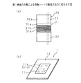
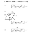
図4は、第1実施の形態による受熱シートの製造方法の工程を示す図である。金属線31bをシリコーンゴム製の基材31aに埋設した伝熱ブロック及びシリコーンゴム製の基材32aに断熱用のフィラー(図示せず)を拡散した断熱ブロックを接合させることにより、1または複数の伝熱体21と1または複数の断熱体22とを結合させた結合体23を作製する(図4(a))。なお、複数の伝熱シート及び断熱シートを積層させて、伝熱体21と断熱体22とを結合させた結合体23を作製しても良い。
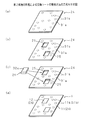
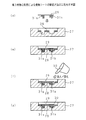
図5は、第2実施の形態による受熱シートの製造方法の工程を示す図である。金属線31bをシリコーンゴム製の基材31aに埋設してなる伝熱シート24を作製する(図5(a))。次いで、伝熱シート24の所定領域に打ち抜き加工を施して、1または複数の孔25を形成する(図5(b))。
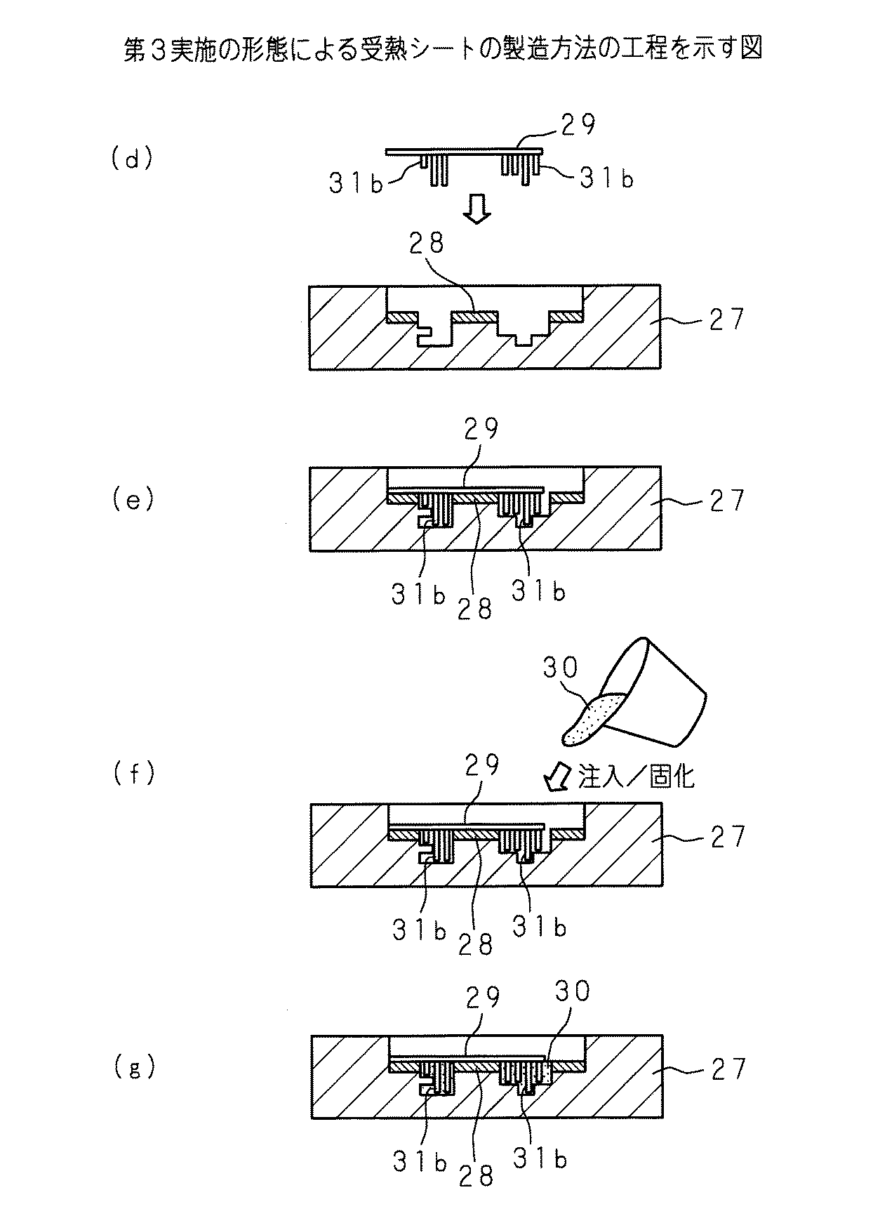
図6及び図7は、第3実施の形態による受熱シートの製造方法の工程を示す図である。製造する受熱シートの形状に合わせて成形された金型27を作製する(図6(a))。次いで、シリコーンゴム製の基材32aに断熱用のフィラー(図示せず)を拡散してなり、1または複数の孔25が形成された断熱シート28を、金型27内に設置する(図6(b),(c))。
(付記1)複数の発熱体で発生した熱を受ける受熱シートにおいて、伝熱部分と断熱部分とを有することを特徴とする受熱シート。
(付記2)前記伝熱部分は、シリコーンゴムからなる基材に金属線を埋設した構成をなすことを特徴とする付記1記載の受熱シート。
(付記3)前記断熱部分は、シリコーンゴムからなる基材に中空体を拡散した構成をなすことを特徴とする付記1または2記載の受熱シート。
(付記4)複数の電子部品で発生した熱を受ける受熱シートを有する電子機器において、前記受熱シートは伝熱部分と断熱部分とを有しており、前記複数の電子部品の中で発熱が大きい第1の電子部品には前記伝熱部分が接触し、前記第1の電子部品の発熱より小さい発熱の第2の電子部品には前記断熱部分が接触するように、前記受熱シートを設けてあることを特徴とする電子機器。
(付記5)前記伝熱部分及び前記断熱部分の厚さは、接触する発熱が大きい前記第1の電子部品及び発熱が小さい前記第2の電子部品の高さに応じて設定してあることを特徴とする付記4記載の電子機器。
(付記6)前記伝熱部分は、シリコーンゴムからなる基材に金属線を埋設した構成をなしており、前記金属線を熱流の方向に配向させていることを特徴とする付記4または5記載の電子機器。
(付記7)伝熱部分と断熱部分とを有する受熱シートを製造する方法であって、1または複数の伝熱体と1または複数の断熱体とを結合して結合体を作製し、作製した結合体からなることを特徴とする受熱シートの製造方法。
(付記8)伝熱部分と断熱部分とを有する受熱シートを製造する方法であって、シート状の伝熱体または断熱体に孔を開け、開けた孔にシート状の断熱体または伝熱体を嵌め込むことを特徴とする受熱シートの製造方法。
(付記9)伝熱部分と断熱部分とを有する受熱シートを製造する方法であって、前記受熱シートの金型を作製し、作製した金型に、1または複数の孔が開けられたシート状の伝熱体または断熱体を設置し、前記孔にシート状の断熱体または伝熱体を形成することを特徴とする受熱シートの製造方法。
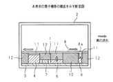
2 筐体
3 プリント基板
4,5,6 電子部品(発熱部品)
7 電子部品(低温部品)
8 中子部材
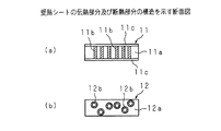
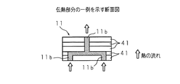
11 伝熱部分
11a,31a 基材
11b,31b 金属線
12 断熱部分
12a,32a 基材
12b ガラスバルーン
21 伝熱体
22 断熱体
23 結合体
24 伝熱シート
25 孔
26 断熱ピース
27 金型
28 断熱シート
Claims (5)
- 複数の発熱体で発生した熱を受ける受熱シートにおいて、シリコーンゴムからなる基材に金属線を埋設した構成をなす伝熱部分とシリコーンゴムからなる基材に中空体を拡散した構成をなす断熱部分とを有することを特徴とする受熱シート。
- 複数の電子部品で発生した熱を受ける受熱シートを有する電子機器において、前記受熱シートはシリコーンゴムからなる基材に金属線を埋設した構成をなす伝熱部分とシリコーンゴムからなる基材に中空体を拡散した構成をなす断熱部分とを有しており、前記複数の電子部品の中で発熱が大きい第1の電子部品には前記伝熱部分が接触し、前記第1の電子部品の発熱より小さい発熱の第2の電子部品には前記断熱部分が接触するように、前記受熱シートを設けてあることを特徴とする電子機器。
- 伝熱部分と断熱部分とを有する受熱シートを製造する方法であって、シリコーンゴムからなる基材に金属線を埋設した構成をなす1または複数の伝熱体とシリコーンゴムからなる基材に中空体を拡散した構成をなす1または複数の断熱体とを結合して結合体を作製し、作製した結合体からなることを特徴とする受熱シートの製造方法。
- 伝熱部分と断熱部分とを有する受熱シートを製造する方法であって、シート状のシリコーンゴムからなる基材に金属線を埋設した構成をなす伝熱体またはシリコーンゴムからなる基材に中空体を拡散した構成をなす断熱体に孔を開け、開けた孔にシート状の断熱体または伝熱体を嵌め込むことを特徴とする受熱シートの製造方法。
- 伝熱部分と断熱部分とを有する受熱シートを製造する方法であって、前記受熱シートの金型を作製し、作製した金型に、1または複数の孔が開けられたシート状の伝熱体または断熱体を設置し、前記孔にシート状の断熱体または伝熱体を形成することを特徴とする受熱シートの製造方法。
Priority Applications (4)
| Application Number | Priority Date | Filing Date | Title |
|---|---|---|---|
| JP2005084794A JP4265796B2 (ja) | 2005-03-23 | 2005-03-23 | 受熱シート、電子機器及び受熱シートの製造方法 |
| US11/181,789 US7295438B2 (en) | 2005-03-23 | 2005-07-15 | Heat receiving sheet, electronic apparatus, and fabrication method for heat receiving sheet |
| KR1020050069188A KR100699972B1 (ko) | 2005-03-23 | 2005-07-29 | 수열 시트, 전자 기기 및 수열 시트의 제조 방법 |
| CN2005100876971A CN1838405B (zh) | 2005-03-23 | 2005-07-29 | 受热片、电子设备以及受热片的制造方法 |
Applications Claiming Priority (1)
| Application Number | Priority Date | Filing Date | Title |
|---|---|---|---|
| JP2005084794A JP4265796B2 (ja) | 2005-03-23 | 2005-03-23 | 受熱シート、電子機器及び受熱シートの製造方法 |
Publications (2)
| Publication Number | Publication Date |
|---|---|
| JP2006269685A JP2006269685A (ja) | 2006-10-05 |
| JP4265796B2 true JP4265796B2 (ja) | 2009-05-20 |
Family
ID=37015723
Family Applications (1)
| Application Number | Title | Priority Date | Filing Date |
|---|---|---|---|
| JP2005084794A Expired - Fee Related JP4265796B2 (ja) | 2005-03-23 | 2005-03-23 | 受熱シート、電子機器及び受熱シートの製造方法 |
Country Status (4)
| Country | Link |
|---|---|
| US (1) | US7295438B2 (ja) |
| JP (1) | JP4265796B2 (ja) |
| KR (1) | KR100699972B1 (ja) |
| CN (1) | CN1838405B (ja) |
Families Citing this family (13)
| Publication number | Priority date | Publication date | Assignee | Title |
|---|---|---|---|---|
| WO2010034411A1 (de) * | 2008-09-24 | 2010-04-01 | Johnson Controls Interiors Gmbh & Co. Kg | Werkzeug und verfahren zur herstellung von flächigen gegenständen mit anbauteilen |
| CN102781199B (zh) * | 2011-05-10 | 2016-03-30 | 华为终端有限公司 | 一种电子元件的保护方法及终端设备 |
| JP2013128034A (ja) * | 2011-12-19 | 2013-06-27 | Seiwa Electric Mfg Co Ltd | 熱対策シート |
| JP5851878B2 (ja) | 2012-02-21 | 2016-02-03 | ルネサスエレクトロニクス株式会社 | 半導体モジュールの製造方法 |
| JP2013254791A (ja) * | 2012-06-05 | 2013-12-19 | Nec Corp | 放熱機構およびその放熱機構を備えた電子機器 |
| CN103635063A (zh) * | 2012-08-21 | 2014-03-12 | 富瑞精密组件(昆山)有限公司 | 散热器组合 |
| TWI624640B (zh) * | 2017-01-25 | 2018-05-21 | 雙鴻科技股份有限公司 | 液冷式散熱裝置 |
| CN108631822A (zh) * | 2018-04-16 | 2018-10-09 | 岫岩满族自治县萤石科技有限公司 | 一种电力线载波通信无线wifi设备 |
| US10856443B2 (en) * | 2018-06-06 | 2020-12-01 | Apple Inc. | Cladded metal structures for dissipation of heat in a portable electronic device |
| KR102808639B1 (ko) * | 2019-05-10 | 2025-05-20 | 삼성전자주식회사 | 열전달 구조를 포함하는 전자 장치 |
| JP6885438B2 (ja) * | 2019-09-24 | 2021-06-16 | カシオ計算機株式会社 | 電子機器 |
| JP7069238B2 (ja) * | 2020-03-17 | 2022-05-17 | 株式会社クボタ | 電子制御装置 |
| JP2024176215A (ja) * | 2023-06-08 | 2024-12-19 | 株式会社オートネットワーク技術研究所 | 車載用電子機器 |
Family Cites Families (10)
| Publication number | Priority date | Publication date | Assignee | Title |
|---|---|---|---|---|
| US5305186A (en) * | 1993-01-27 | 1994-04-19 | International Business Machines Corporation | Power carrier with selective thermal performance |
| JPH07149365A (ja) * | 1993-11-26 | 1995-06-13 | Denki Kagaku Kogyo Kk | 絶縁放熱シート包装体、及び基板又は放熱フィン |
| JPH1126968A (ja) | 1997-07-09 | 1999-01-29 | Asia Electron Inc | 基板の冷却装置及び基板放熱用スペーサ |
| JP3444199B2 (ja) * | 1998-06-17 | 2003-09-08 | 信越化学工業株式会社 | 熱伝導性シリコーンゴム組成物及びその製造方法 |
| JP2000077872A (ja) * | 1998-08-27 | 2000-03-14 | Nitto Denko Corp | 熱伝導部材及び当該伝導部材を用いた電子機器 |
| JP3543663B2 (ja) * | 1999-03-11 | 2004-07-14 | 信越化学工業株式会社 | 熱伝導性シリコーンゴム組成物及びその製造方法 |
| JP4301468B2 (ja) * | 1999-07-07 | 2009-07-22 | 信越化学工業株式会社 | 耐熱熱伝導性シリコーンゴム複合シート及びその製造方法 |
| TW555794B (en) * | 2000-02-29 | 2003-10-01 | Shinetsu Chemical Co | Method for the preparation of low specific gravity silicone rubber elastomers |
| JP2001270021A (ja) | 2000-03-23 | 2001-10-02 | Fujimori Kogyo Co Ltd | 反射断熱シート |
| EP1233666A4 (en) * | 2000-06-06 | 2005-04-13 | Mitsubishi Electric Corp | COOLING STRUCTURE OF A COMMUNICATION DEVICE |
-
2005
- 2005-03-23 JP JP2005084794A patent/JP4265796B2/ja not_active Expired - Fee Related
- 2005-07-15 US US11/181,789 patent/US7295438B2/en not_active Expired - Fee Related
- 2005-07-29 KR KR1020050069188A patent/KR100699972B1/ko not_active Expired - Fee Related
- 2005-07-29 CN CN2005100876971A patent/CN1838405B/zh not_active Expired - Fee Related
Also Published As
| Publication number | Publication date |
|---|---|
| CN1838405A (zh) | 2006-09-27 |
| US20060215371A1 (en) | 2006-09-28 |
| KR20060102469A (ko) | 2006-09-27 |
| JP2006269685A (ja) | 2006-10-05 |
| US7295438B2 (en) | 2007-11-13 |
| CN1838405B (zh) | 2012-03-07 |
| KR100699972B1 (ko) | 2007-03-27 |
Similar Documents
| Publication | Publication Date | Title |
|---|---|---|
| JP4265796B2 (ja) | 受熱シート、電子機器及び受熱シートの製造方法 | |
| KR101538944B1 (ko) | 유연한 적층 열도전성 계면 조립체 및 이를 포함하는 메모리 모듈 | |
| US8004846B2 (en) | Heat radiator | |
| US9222735B2 (en) | Compliant multilayered thermally-conductive interface assemblies | |
| CN102036466A (zh) | 刚性-柔性电路板以及制造该电路板的方法 | |
| JP6862896B2 (ja) | 半導体装置及び半導体装置の製造方法 | |
| US20090139690A1 (en) | Heat sink and method for producing a heat sink | |
| US20140262449A1 (en) | Apparatus and Method for a Back Plate for Heat Sink Mounting | |
| US20100321897A1 (en) | Compliant multilayered thermally-conductive interface assemblies | |
| CN101513150A (zh) | 马达控制器 | |
| JP2010251386A (ja) | 熱拡散部材を備える電子機器、熱拡散部材を備える電子機器の製法及び熱拡散部材 | |
| WO2016067383A1 (ja) | 放熱構造 | |
| JP2002033558A (ja) | 回路基板とその製造方法 | |
| JP2014187233A (ja) | 放熱シートおよびこれを用いた放熱構造 | |
| CN102404976A (zh) | 电子装置 | |
| JP2008218618A (ja) | プリント配線板 | |
| JP2020174116A (ja) | ヒートシンク固定部材及び電子装置 | |
| JP2008205344A (ja) | 熱伝導基板とその製造方法及びこれを用いた回路モジュール | |
| CN104350592A (zh) | 用于在安装具有导热垫的组件时减少机械应力的方法和装置 | |
| JP2008258527A (ja) | 放熱装置 | |
| CN102802379B (zh) | 散热组件及电子设备 | |
| CN112310019A (zh) | 包括用于热管理的石墨烯层的存储器模块和存储器封装 | |
| JP5279639B2 (ja) | グラファイトシート | |
| KR20150143578A (ko) | 프린트 배선판 및 그의 제조방법, 및 전열체 | |
| JP4325329B2 (ja) | 放熱実装体 |
Legal Events
| Date | Code | Title | Description |
|---|---|---|---|
| A621 | Written request for application examination |
Free format text: JAPANESE INTERMEDIATE CODE: A621 Effective date: 20060714 |
|
| A977 | Report on retrieval |
Free format text: JAPANESE INTERMEDIATE CODE: A971007 Effective date: 20081022 |
|
| A131 | Notification of reasons for refusal |
Free format text: JAPANESE INTERMEDIATE CODE: A131 Effective date: 20081028 |
|
| A521 | Request for written amendment filed |
Free format text: JAPANESE INTERMEDIATE CODE: A523 Effective date: 20081225 |
|
| TRDD | Decision of grant or rejection written | ||
| A01 | Written decision to grant a patent or to grant a registration (utility model) |
Free format text: JAPANESE INTERMEDIATE CODE: A01 Effective date: 20090210 |
|
| A01 | Written decision to grant a patent or to grant a registration (utility model) |
Free format text: JAPANESE INTERMEDIATE CODE: A01 |
|
| A61 | First payment of annual fees (during grant procedure) |
Free format text: JAPANESE INTERMEDIATE CODE: A61 Effective date: 20090210 |
|
| R150 | Certificate of patent or registration of utility model |
Free format text: JAPANESE INTERMEDIATE CODE: R150 |
|
| FPAY | Renewal fee payment (event date is renewal date of database) |
Free format text: PAYMENT UNTIL: 20120227 Year of fee payment: 3 |
|
| FPAY | Renewal fee payment (event date is renewal date of database) |
Free format text: PAYMENT UNTIL: 20130227 Year of fee payment: 4 |
|
| FPAY | Renewal fee payment (event date is renewal date of database) |
Free format text: PAYMENT UNTIL: 20140227 Year of fee payment: 5 |
|
| LAPS | Cancellation because of no payment of annual fees |