JP4261440B2 - 伝送回路基板 - Google Patents
伝送回路基板 Download PDFInfo
- Publication number
- JP4261440B2 JP4261440B2 JP2004249442A JP2004249442A JP4261440B2 JP 4261440 B2 JP4261440 B2 JP 4261440B2 JP 2004249442 A JP2004249442 A JP 2004249442A JP 2004249442 A JP2004249442 A JP 2004249442A JP 4261440 B2 JP4261440 B2 JP 4261440B2
- Authority
- JP
- Japan
- Prior art keywords
- signal
- row
- layer
- terminal
- portions
- Prior art date
- Legal status (The legal status is an assumption and is not a legal conclusion. Google has not performed a legal analysis and makes no representation as to the accuracy of the status listed.)
- Expired - Fee Related
Links
Images


Classifications
-
- H—ELECTRICITY
- H05—ELECTRIC TECHNIQUES NOT OTHERWISE PROVIDED FOR
- H05K—PRINTED CIRCUITS; CASINGS OR CONSTRUCTIONAL DETAILS OF ELECTRIC APPARATUS; MANUFACTURE OF ASSEMBLAGES OF ELECTRICAL COMPONENTS
- H05K1/00—Printed circuits
- H05K1/02—Details
- H05K1/11—Printed elements for providing electric connections to or between printed circuits
- H05K1/115—Via connections; Lands around holes or via connections
- H05K1/116—Lands, clearance holes or other lay-out details concerning the surrounding of a via
-
- H—ELECTRICITY
- H05—ELECTRIC TECHNIQUES NOT OTHERWISE PROVIDED FOR
- H05K—PRINTED CIRCUITS; CASINGS OR CONSTRUCTIONAL DETAILS OF ELECTRIC APPARATUS; MANUFACTURE OF ASSEMBLAGES OF ELECTRICAL COMPONENTS
- H05K1/00—Printed circuits
- H05K1/02—Details
- H05K1/0213—Electrical arrangements not otherwise provided for
- H05K1/0216—Reduction of cross-talk, noise or electromagnetic interference
- H05K1/0218—Reduction of cross-talk, noise or electromagnetic interference by printed shielding conductors, ground planes or power plane
-
- H—ELECTRICITY
- H01—ELECTRIC ELEMENTS
- H01L—SEMICONDUCTOR DEVICES NOT COVERED BY CLASS H10
- H01L23/00—Details of semiconductor or other solid state devices
- H01L23/48—Arrangements for conducting electric current to or from the solid state body in operation, e.g. leads, terminal arrangements ; Selection of materials therefor
- H01L23/488—Arrangements for conducting electric current to or from the solid state body in operation, e.g. leads, terminal arrangements ; Selection of materials therefor consisting of soldered or bonded constructions
- H01L23/498—Leads, i.e. metallisations or lead-frames on insulating substrates, e.g. chip carriers
- H01L23/49838—Geometry or layout
-
- H—ELECTRICITY
- H01—ELECTRIC ELEMENTS
- H01L—SEMICONDUCTOR DEVICES NOT COVERED BY CLASS H10
- H01L2924/00—Indexing scheme for arrangements or methods for connecting or disconnecting semiconductor or solid-state bodies as covered by H01L24/00
- H01L2924/0001—Technical content checked by a classifier
- H01L2924/0002—Not covered by any one of groups H01L24/00, H01L24/00 and H01L2224/00
-
- H—ELECTRICITY
- H05—ELECTRIC TECHNIQUES NOT OTHERWISE PROVIDED FOR
- H05K—PRINTED CIRCUITS; CASINGS OR CONSTRUCTIONAL DETAILS OF ELECTRIC APPARATUS; MANUFACTURE OF ASSEMBLAGES OF ELECTRICAL COMPONENTS
- H05K1/00—Printed circuits
- H05K1/02—Details
- H05K1/0296—Conductive pattern lay-out details not covered by sub groups H05K1/02 - H05K1/0295
- H05K1/0298—Multilayer circuits
-
- H—ELECTRICITY
- H05—ELECTRIC TECHNIQUES NOT OTHERWISE PROVIDED FOR
- H05K—PRINTED CIRCUITS; CASINGS OR CONSTRUCTIONAL DETAILS OF ELECTRIC APPARATUS; MANUFACTURE OF ASSEMBLAGES OF ELECTRICAL COMPONENTS
- H05K1/00—Printed circuits
- H05K1/18—Printed circuits structurally associated with non-printed electric components
-
- H—ELECTRICITY
- H05—ELECTRIC TECHNIQUES NOT OTHERWISE PROVIDED FOR
- H05K—PRINTED CIRCUITS; CASINGS OR CONSTRUCTIONAL DETAILS OF ELECTRIC APPARATUS; MANUFACTURE OF ASSEMBLAGES OF ELECTRICAL COMPONENTS
- H05K2201/00—Indexing scheme relating to printed circuits covered by H05K1/00
- H05K2201/07—Electric details
- H05K2201/0707—Shielding
- H05K2201/0715—Shielding provided by an outer layer of PCB
-
- H—ELECTRICITY
- H05—ELECTRIC TECHNIQUES NOT OTHERWISE PROVIDED FOR
- H05K—PRINTED CIRCUITS; CASINGS OR CONSTRUCTIONAL DETAILS OF ELECTRIC APPARATUS; MANUFACTURE OF ASSEMBLAGES OF ELECTRICAL COMPONENTS
- H05K2201/00—Indexing scheme relating to printed circuits covered by H05K1/00
- H05K2201/09—Shape and layout
- H05K2201/09209—Shape and layout details of conductors
- H05K2201/09218—Conductive traces
- H05K2201/09236—Parallel layout
-
- H—ELECTRICITY
- H05—ELECTRIC TECHNIQUES NOT OTHERWISE PROVIDED FOR
- H05K—PRINTED CIRCUITS; CASINGS OR CONSTRUCTIONAL DETAILS OF ELECTRIC APPARATUS; MANUFACTURE OF ASSEMBLAGES OF ELECTRICAL COMPONENTS
- H05K2201/00—Indexing scheme relating to printed circuits covered by H05K1/00
- H05K2201/09—Shape and layout
- H05K2201/09209—Shape and layout details of conductors
- H05K2201/095—Conductive through-holes or vias
- H05K2201/09609—Via grid, i.e. two-dimensional array of vias or holes in a single plane
-
- H—ELECTRICITY
- H05—ELECTRIC TECHNIQUES NOT OTHERWISE PROVIDED FOR
- H05K—PRINTED CIRCUITS; CASINGS OR CONSTRUCTIONAL DETAILS OF ELECTRIC APPARATUS; MANUFACTURE OF ASSEMBLAGES OF ELECTRICAL COMPONENTS
- H05K2201/00—Indexing scheme relating to printed circuits covered by H05K1/00
- H05K2201/10—Details of components or other objects attached to or integrated in a printed circuit board
- H05K2201/10007—Types of components
- H05K2201/10189—Non-printed connector
-
- H—ELECTRICITY
- H05—ELECTRIC TECHNIQUES NOT OTHERWISE PROVIDED FOR
- H05K—PRINTED CIRCUITS; CASINGS OR CONSTRUCTIONAL DETAILS OF ELECTRIC APPARATUS; MANUFACTURE OF ASSEMBLAGES OF ELECTRICAL COMPONENTS
- H05K3/00—Apparatus or processes for manufacturing printed circuits
- H05K3/40—Forming printed elements for providing electric connections to or between printed circuits
- H05K3/42—Plated through-holes or plated via connections
- H05K3/429—Plated through-holes specially for multilayer circuits, e.g. having connections to inner circuit layers
Description
米国、ALTERA社技術資料(2000年7月)「Board Design Guidelines for LVDS Systems」
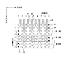
本実施形態の伝送回路基板における端子部の配列の様子を図1に示す。この配列は本発明の基本であり、以降の他の実施形態においても共通である。
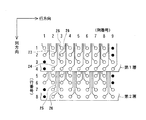
図4に示す第二実施形態では、伝送回路基板が8行の信号用端子部を2層に収めている点では、第一実施形態と同じであるが、第一層における信号用端子部が対をなしていない点で相違している。第二層については、第一実施形態と同じである。
図5に示した第三実施形態では、信号用端子部20は隣接せる二つの奇数行、そして隣接せる二つの偶数行で、それぞれ信号回路層をなしている点に特徴がある。
図6に示される第四実施形態では、図2の第一実施形態のパターンと図5の第三実施形態のパターンとが組み合されている点に特徴がある。すなわち、図6では、信号回路層は第一ないし第三層から成っていて、第一層が図2の第一層や第二層と同じパターンであり、図6の第二層と第三層が図5における第一層と第二層と同じパターンとなっている。
図7に示される第五実施形態は、第四実施形態よりもさらに複雑に各種パターンが組み合されている。図7では、信号回路層は、第一ないし第三層から成っている。第一層は左半分の第一列ないし第五列(ただし、第五列は第三、四行のみ)が図4の第二実施形態の第一層の第一列ないし第五列(ただし、第五列は第三、四行のみ)と同じ、そして右半分の第五列(第一、二行)ないし第九列が図2の第一実施形態の第一層の第五列(第一、二行)ないし第九列と同じパターンである。
20 信号用端子部
20A 信号用接続部
21,22 配線部
Claims (4)
- 絶縁板中に設けられた複数の信号回路層と各信号回路層を覆うグランド層とを絶縁層を介して有し、板厚方向にこれらの層の少なくとも一層を貫通して延びる導電性の端子部が基板面で複数の行及び列をなす位置に設けられ、端子部は両端列に位置する一部の数の端子部がグランド用端子部として、そして他の端子部の少なくとも一部は信号用端子部としてそれぞれ形成され、信号回路層は、層同士間で重ならない行列位置で、信号用端子部の周面から延出せる信号用接続部と該信号用接続部から発して基板の端部へ列方向に延びて形成された配線部とを有し、グランド層は上記信号用端子部の外周面と間隔をもって基板面に平行な面状に形成されかつグランド端子部と導通している伝送回路基板において、グランド用端子部は両端列にて二行毎に設けられ、各信号回路層は、信号回路層同士で異なる列方向又は行方向で、隣接する少なくとも一対をなす信号用接続部が平行な一対の配線部と導通しており、各グランド層は両端列でそれぞれ少なくとも一つのグランド用端子部と導通していることを特徴とする伝送回路基板。
- 信号回路層は伝送基板の少なくとも一部の領域で四行毎に一層をなし、少なくとも該一層にて、一対をなす信号用接続部が列方向で隣接していることとする請求項1に記載の伝送回路基板。
- 一層内に存在する四行の信号用接続部は、第一行及び第二行で列位置が同一で、第三行及び第四行とで上記第一行及び第二行での列位置に対して一列ずれた位置にあり、各行で列方向に隣接して対をなす信号用接続部から発する一対の配線部が列方向に延びており、第一行と第二行の配線部と第三行と第四行の配線部とが異なる列間に配されていることとする請求項2に記載の伝送回路基板。
- 絶縁板中に設けられた複数の信号回路層と各信号回路層を覆うグランド層とを絶縁層を介して有し、板厚方向にこれらの層の少なくとも一層を貫通して延びる導電性の端子部が基板面で複数の行及び列をなす位置に設けられ、端子部は両端列に位置する一部の数の端子部がグランド用端子部として、そして他の端子部の少なくとも一部は信号用端子部としてそれぞれ形成され、信号回路層は、層同士間で重ならない行列位置で、信号用端子部の周面から延出せる信号用接続部と該信号用接続部から発して基板の端部へ列方向に延びて形成された配線部とを有し、グランド層は上記信号用端子部の外周面と間隔をもって基板面に平行な面状に形成されかつグランド端子部と導通している伝送回路基板と、該伝送回路基板に接続されたコネクタとを有するコネクタ装置において、伝送回路基板は、グランド用端子部が両端列にて二行毎に設けられ、各信号回路層は、信号回路層同士で異なる列方向又は行方向で、隣接する少なくとも一対をなす信号用接続部が平行な一対の配線部と導通しており、各グランド層は両端列でそれぞれ少なくとも一つのグランド用端子部と導通しており、コネクタのグランド端子と信号端子が上記伝送用回路基板のそれぞれ対応するグランド用端子部と信号用端子とに接続されていることを特徴とする伝送回路基板付コネクタ装置。
Priority Applications (3)
| Application Number | Priority Date | Filing Date | Title |
|---|---|---|---|
| JP2004249442A JP4261440B2 (ja) | 2004-08-30 | 2004-08-30 | 伝送回路基板 |
| US11/201,104 US7329818B2 (en) | 2004-08-30 | 2005-08-11 | Transmission circuit board |
| EP05018486A EP1631130A3 (en) | 2004-08-30 | 2005-08-25 | Transmission circuit board |
Applications Claiming Priority (1)
| Application Number | Priority Date | Filing Date | Title |
|---|---|---|---|
| JP2004249442A JP4261440B2 (ja) | 2004-08-30 | 2004-08-30 | 伝送回路基板 |
Publications (2)
| Publication Number | Publication Date |
|---|---|
| JP2006066753A JP2006066753A (ja) | 2006-03-09 |
| JP4261440B2 true JP4261440B2 (ja) | 2009-04-30 |
Family
ID=35431046
Family Applications (1)
| Application Number | Title | Priority Date | Filing Date |
|---|---|---|---|
| JP2004249442A Expired - Fee Related JP4261440B2 (ja) | 2004-08-30 | 2004-08-30 | 伝送回路基板 |
Country Status (3)
| Country | Link |
|---|---|
| US (1) | US7329818B2 (ja) |
| EP (1) | EP1631130A3 (ja) |
| JP (1) | JP4261440B2 (ja) |
Families Citing this family (8)
| Publication number | Priority date | Publication date | Assignee | Title |
|---|---|---|---|---|
| JP4354489B2 (ja) * | 2004-02-13 | 2009-10-28 | モレックス インコーポレイテド | 回路基板及び高速ビアシステム |
| US7441222B2 (en) * | 2006-09-29 | 2008-10-21 | Nokia Corporation | Differential pair connection arrangement, and method and computer program product for making same |
| JP5107270B2 (ja) * | 2007-02-07 | 2012-12-26 | ローム株式会社 | 実装基板および電子機器 |
| JP2009043786A (ja) * | 2007-08-06 | 2009-02-26 | Rohm Co Ltd | 実装基板および電子部品 |
| FR2950219A1 (fr) * | 2009-09-11 | 2011-03-18 | Thales Sa | Interconnexion pour circuit imprime haute frequence |
| JP2011239040A (ja) * | 2010-05-06 | 2011-11-24 | Canon Inc | 撮像装置 |
| US10477672B2 (en) * | 2018-01-29 | 2019-11-12 | Hewlett Packard Enterprise Development Lp | Single ended vias with shared voids |
| KR102310198B1 (ko) * | 2018-07-16 | 2021-10-08 | 엘에스엠트론 주식회사 | 광커넥터 및 이를 포함하는 전자장치 |
Family Cites Families (6)
| Publication number | Priority date | Publication date | Assignee | Title |
|---|---|---|---|---|
| JP3014503B2 (ja) * | 1991-08-05 | 2000-02-28 | 日本特殊陶業株式会社 | 集積回路用パッケージ |
| JPH1174399A (ja) | 1997-08-28 | 1999-03-16 | Mitsubishi Electric Corp | 半導体装置 |
| JP3784188B2 (ja) * | 1999-01-21 | 2006-06-07 | 京セラ株式会社 | 電子部品搭載用配線基板 |
| JP3425898B2 (ja) * | 1999-07-09 | 2003-07-14 | Necエレクトロニクス株式会社 | エリアアレイ型半導体装置 |
| US7069650B2 (en) * | 2000-06-19 | 2006-07-04 | Nortel Networks Limited | Method for reducing the number of layers in a multilayer signal routing device |
| US6744130B1 (en) * | 2003-07-08 | 2004-06-01 | Lsi Logic Corporation | Isolated stripline structure |
-
2004
- 2004-08-30 JP JP2004249442A patent/JP4261440B2/ja not_active Expired - Fee Related
-
2005
- 2005-08-11 US US11/201,104 patent/US7329818B2/en not_active Expired - Fee Related
- 2005-08-25 EP EP05018486A patent/EP1631130A3/en not_active Withdrawn
Also Published As
| Publication number | Publication date |
|---|---|
| JP2006066753A (ja) | 2006-03-09 |
| EP1631130A3 (en) | 2007-08-08 |
| US7329818B2 (en) | 2008-02-12 |
| EP1631130A2 (en) | 2006-03-01 |
| US20060042828A1 (en) | 2006-03-02 |
Similar Documents
| Publication | Publication Date | Title |
|---|---|---|
| JP4439540B2 (ja) | コネクタ | |
| US7872852B2 (en) | Conductive structure having capacitor | |
| US7329818B2 (en) | Transmission circuit board | |
| CN101836336B (zh) | 板安装型电连接器 | |
| JP5204895B2 (ja) | 信号伝送ラインの周りのボンディングシートを除去した印刷回路基板 | |
| KR101478938B1 (ko) | 커넥터 | |
| CN105487719A (zh) | 集成触控显示面板和包含其的集成触控显示装置 | |
| JP2016508675A (ja) | 差動信号ルーティングを偏倚したプリント回路基板(pcb) | |
| CN104956776A (zh) | 具有正交信号通路的印刷电路板 | |
| KR19990062589A (ko) | 다층 회로 기판 | |
| CN105788466A (zh) | 一种显示面板、其制作方法及显示装置 | |
| CN101112135A (zh) | 改进的匹配阻抗表面贴装技术基底面 | |
| JP6692455B2 (ja) | 差動コネクタおよびその差動対配置構造ならびに差動コネクタプラグ | |
| JP2013080628A (ja) | 配線板、コネクタおよび電子装置 | |
| JP2013172017A (ja) | 多層配線基板及び電子機器 | |
| TW201419101A (zh) | 觸控面板 | |
| EP1075026A2 (en) | Multilayer circuit board layout | |
| KR20040087876A (ko) | 다층 신호라우팅 디바이스에서 층수를 줄이는 기술 | |
| JP2005101082A (ja) | ランドパターン構造 | |
| CN209914166U (zh) | 一种阵列焊盘差分布线结构及连接器封装 | |
| TWI661245B (zh) | 顯示面板 | |
| JP2007294768A (ja) | 半導体装置 | |
| JP5006640B2 (ja) | 半導体装置の製造方法 | |
| KR102135886B1 (ko) | 터치 패널 및 터치 패널의 생산 방법 | |
| JP6133024B2 (ja) | 光モジュール |
Legal Events
| Date | Code | Title | Description |
|---|---|---|---|
| A621 | Written request for application examination |
Free format text: JAPANESE INTERMEDIATE CODE: A621 Effective date: 20060804 |
|
| A977 | Report on retrieval |
Free format text: JAPANESE INTERMEDIATE CODE: A971007 Effective date: 20081016 |
|
| A131 | Notification of reasons for refusal |
Free format text: JAPANESE INTERMEDIATE CODE: A131 Effective date: 20081023 |
|
| A521 | Written amendment |
Free format text: JAPANESE INTERMEDIATE CODE: A523 Effective date: 20081208 |
|
| TRDD | Decision of grant or rejection written | ||
| A01 | Written decision to grant a patent or to grant a registration (utility model) |
Free format text: JAPANESE INTERMEDIATE CODE: A01 Effective date: 20090204 |
|
| A01 | Written decision to grant a patent or to grant a registration (utility model) |
Free format text: JAPANESE INTERMEDIATE CODE: A01 |
|
| A61 | First payment of annual fees (during grant procedure) |
Free format text: JAPANESE INTERMEDIATE CODE: A61 Effective date: 20090205 |
|
| FPAY | Renewal fee payment (event date is renewal date of database) |
Free format text: PAYMENT UNTIL: 20120220 Year of fee payment: 3 |
|
| R150 | Certificate of patent or registration of utility model |
Ref document number: 4261440 Country of ref document: JP Free format text: JAPANESE INTERMEDIATE CODE: R150 Free format text: JAPANESE INTERMEDIATE CODE: R150 |
|
| FPAY | Renewal fee payment (event date is renewal date of database) |
Free format text: PAYMENT UNTIL: 20120220 Year of fee payment: 3 |
|
| FPAY | Renewal fee payment (event date is renewal date of database) |
Free format text: PAYMENT UNTIL: 20120220 Year of fee payment: 3 |
|
| FPAY | Renewal fee payment (event date is renewal date of database) |
Free format text: PAYMENT UNTIL: 20120220 Year of fee payment: 3 |
|
| FPAY | Renewal fee payment (event date is renewal date of database) |
Free format text: PAYMENT UNTIL: 20130220 Year of fee payment: 4 |
|
| R250 | Receipt of annual fees |
Free format text: JAPANESE INTERMEDIATE CODE: R250 |
|
| FPAY | Renewal fee payment (event date is renewal date of database) |
Free format text: PAYMENT UNTIL: 20130220 Year of fee payment: 4 |
|
| FPAY | Renewal fee payment (event date is renewal date of database) |
Free format text: PAYMENT UNTIL: 20140220 Year of fee payment: 5 |
|
| R250 | Receipt of annual fees |
Free format text: JAPANESE INTERMEDIATE CODE: R250 |
|
| R250 | Receipt of annual fees |
Free format text: JAPANESE INTERMEDIATE CODE: R250 |
|
| R250 | Receipt of annual fees |
Free format text: JAPANESE INTERMEDIATE CODE: R250 |
|
| R250 | Receipt of annual fees |
Free format text: JAPANESE INTERMEDIATE CODE: R250 |
|
| R250 | Receipt of annual fees |
Free format text: JAPANESE INTERMEDIATE CODE: R250 |
|
| R250 | Receipt of annual fees |
Free format text: JAPANESE INTERMEDIATE CODE: R250 |
|
| R250 | Receipt of annual fees |
Free format text: JAPANESE INTERMEDIATE CODE: R250 |
|
| R250 | Receipt of annual fees |
Free format text: JAPANESE INTERMEDIATE CODE: R250 |
|
| LAPS | Cancellation because of no payment of annual fees |