JP3584635B2 - 半導体装置及びその製造方法 - Google Patents
半導体装置及びその製造方法 Download PDFInfo
- Publication number
- JP3584635B2 JP3584635B2 JP26464296A JP26464296A JP3584635B2 JP 3584635 B2 JP3584635 B2 JP 3584635B2 JP 26464296 A JP26464296 A JP 26464296A JP 26464296 A JP26464296 A JP 26464296A JP 3584635 B2 JP3584635 B2 JP 3584635B2
- Authority
- JP
- Japan
- Prior art keywords
- thin film
- silicon
- gold
- substrate
- film
- Prior art date
- Legal status (The legal status is an assumption and is not a legal conclusion. Google has not performed a legal analysis and makes no representation as to the accuracy of the status listed.)
- Expired - Fee Related
Links
Images


Classifications
-
- B—PERFORMING OPERATIONS; TRANSPORTING
- B81—MICROSTRUCTURAL TECHNOLOGY
- B81C—PROCESSES OR APPARATUS SPECIALLY ADAPTED FOR THE MANUFACTURE OR TREATMENT OF MICROSTRUCTURAL DEVICES OR SYSTEMS
- B81C1/00—Manufacture or treatment of devices or systems in or on a substrate
- B81C1/00015—Manufacture or treatment of devices or systems in or on a substrate for manufacturing microsystems
- B81C1/00261—Processes for packaging MEMS devices
- B81C1/00269—Bonding of solid lids or wafers to the substrate
-
- B—PERFORMING OPERATIONS; TRANSPORTING
- B81—MICROSTRUCTURAL TECHNOLOGY
- B81C—PROCESSES OR APPARATUS SPECIALLY ADAPTED FOR THE MANUFACTURE OR TREATMENT OF MICROSTRUCTURAL DEVICES OR SYSTEMS
- B81C1/00—Manufacture or treatment of devices or systems in or on a substrate
- B81C1/00349—Creating layers of material on a substrate
- B81C1/00357—Creating layers of material on a substrate involving bonding one or several substrates on a non-temporary support, e.g. another substrate
-
- B—PERFORMING OPERATIONS; TRANSPORTING
- B81—MICROSTRUCTURAL TECHNOLOGY
- B81C—PROCESSES OR APPARATUS SPECIALLY ADAPTED FOR THE MANUFACTURE OR TREATMENT OF MICROSTRUCTURAL DEVICES OR SYSTEMS
- B81C1/00—Manufacture or treatment of devices or systems in or on a substrate
- B81C1/00865—Multistep processes for the separation of wafers into individual elements
- B81C1/00873—Multistep processes for the separation of wafers into individual elements characterised by special arrangements of the devices, allowing an easier separation
-
- G—PHYSICS
- G01—MEASURING; TESTING
- G01P—MEASURING LINEAR OR ANGULAR SPEED, ACCELERATION, DECELERATION, OR SHOCK; INDICATING PRESENCE, ABSENCE, OR DIRECTION, OF MOVEMENT
- G01P15/00—Measuring acceleration; Measuring deceleration; Measuring shock, i.e. sudden change of acceleration
- G01P15/02—Measuring acceleration; Measuring deceleration; Measuring shock, i.e. sudden change of acceleration by making use of inertia forces using solid seismic masses
- G01P15/08—Measuring acceleration; Measuring deceleration; Measuring shock, i.e. sudden change of acceleration by making use of inertia forces using solid seismic masses with conversion into electric or magnetic values
- G01P15/0802—Details
-
- G—PHYSICS
- G01—MEASURING; TESTING
- G01P—MEASURING LINEAR OR ANGULAR SPEED, ACCELERATION, DECELERATION, OR SHOCK; INDICATING PRESENCE, ABSENCE, OR DIRECTION, OF MOVEMENT
- G01P15/00—Measuring acceleration; Measuring deceleration; Measuring shock, i.e. sudden change of acceleration
- G01P15/02—Measuring acceleration; Measuring deceleration; Measuring shock, i.e. sudden change of acceleration by making use of inertia forces using solid seismic masses
- G01P15/08—Measuring acceleration; Measuring deceleration; Measuring shock, i.e. sudden change of acceleration by making use of inertia forces using solid seismic masses with conversion into electric or magnetic values
- G01P15/12—Measuring acceleration; Measuring deceleration; Measuring shock, i.e. sudden change of acceleration by making use of inertia forces using solid seismic masses with conversion into electric or magnetic values by alteration of electrical resistance
- G01P15/124—Measuring acceleration; Measuring deceleration; Measuring shock, i.e. sudden change of acceleration by making use of inertia forces using solid seismic masses with conversion into electric or magnetic values by alteration of electrical resistance by semiconductor devices comprising at least one PN junction, e.g. transistors
-
- H—ELECTRICITY
- H10—SEMICONDUCTOR DEVICES; ELECTRIC SOLID-STATE DEVICES NOT OTHERWISE PROVIDED FOR
- H10W—GENERIC PACKAGES, INTERCONNECTIONS, CONNECTORS OR OTHER CONSTRUCTIONAL DETAILS OF DEVICES COVERED BY CLASS H10
- H10W76/00—Containers; Fillings or auxiliary members therefor; Seals
- H10W76/60—Seals
-
- B—PERFORMING OPERATIONS; TRANSPORTING
- B81—MICROSTRUCTURAL TECHNOLOGY
- B81C—PROCESSES OR APPARATUS SPECIALLY ADAPTED FOR THE MANUFACTURE OR TREATMENT OF MICROSTRUCTURAL DEVICES OR SYSTEMS
- B81C2201/00—Manufacture or treatment of microstructural devices or systems
- B81C2201/01—Manufacture or treatment of microstructural devices or systems in or on a substrate
- B81C2201/0174—Manufacture or treatment of microstructural devices or systems in or on a substrate for making multi-layered devices, film deposition or growing
- B81C2201/019—Bonding or gluing multiple substrate layers
Landscapes
- Engineering & Computer Science (AREA)
- Microelectronics & Electronic Packaging (AREA)
- Manufacturing & Machinery (AREA)
- Physics & Mathematics (AREA)
- General Physics & Mathematics (AREA)
- Computer Hardware Design (AREA)
- Pressure Sensors (AREA)
Description
【発明の属する技術分野】
この発明は半導体装置及びその製造方法に係り、例えば、機能素子を覆う保護キャップを有する半導体装置等に適用できるものである。
【0002】
【従来の技術】
従来、半導体加速度センサやヨーレイトセンサ等においては、シリコンチップ上に可動部(振動部)を有し、可動部(振動部)の変位により加速度等の物理量を電気信号に変換して取り出すようになっている。又、このような半導体装置において、可動部(振動部)を保護するために可動部をキャップにて覆うことが行われている(例えば、特開平5−326702号公報等)。さらに、検出感度の高感度化、特性の安定性あるいはエアダンピングの回避等を考慮すると可動部周囲の雰囲気としては不活性ガスや還元性ガス、場合によっては真空がよい。以上のことから可動部をこれらの雰囲気で封止する必要性から、リークのないキャップが必要不可欠となる。
【0003】
【発明が解決しようとする課題】
これに対応するようなキャップ形態として特開平5−326702号公報のように可動部を有する構造体をチップごと覆うと小型化には適さない。又、特開平4−304679号公報のように構造体をウェハプロセス中に薄膜で封止する技術もあるが、キャップが薄膜で形成されるために機械的強度が低い、構造体の形状に制限がある、汎用性がない等の欠点がある。キャップの機械的強度を向上するために、薄膜でなくバルクのキャップをチップ上に形成する場合は、接合方法に工夫が必要となるとともに、量産性を考慮した製造方法(キャップの一括接合など)が要求される。
【0004】
接合方法としては陽極接合や直接接合や共晶接合などがあるが、陽極接合では、チップに接合する際に高電圧が印加されるため高耐圧性のない回路素子は破壊されたり(チップに構造体しかない場合は特に問題にならないが、回路素子を別チップで形成する必要があり汎用性のある接合方法とは言えない)、接合時にガスが放出され、センサ特性に影響が出る(特に真空封止においては真空度が劣化する)。又、直接接合では原子レベルで密着させる必要性から現状では極限られた範囲しか適用されておらず、接合に関わる表面の平坦性が要求されたり、高加圧力で密着させる必要から汎用的な方法とは言えず、この場合も適用し難い。
【0005】
さらに、共晶接合は歴史的に古い接合方法ではあるが、接合部が液化することから加圧力も低くなり、Au/Si共晶接合法においては接合温度も低く、プロセスとの整合性もあることからキャップの接合方法として最も有効的と考えられるが、共晶反応はボイドが生じやすい欠点がある。ボイドが形成されるとその発生箇所によってはリークが生じる。現在、ボイドレスな接合を高歩留まりで確立したという報告はない。又、Au/Si共晶接合法においてSi(シリコン)は極めて活性な物質であるためにシリコンの表面には自然酸化膜が形成され、この酸化膜によりシリコンとAu(金)との界面において全域において共晶領域が形成されておらず接合の強度が大きくばらついてしまう。
【0006】
そこで、この発明の目的は、Au/Si共晶による接合箇所においてシリコンの表面に形成される自然酸化膜による不具合を解消することができる半導体装置及びその製造方法を提供することにある。
【0007】
【課題を解決するための手段】
請求項2に記載の発明によれば、第1工程により、第2の基板における少なくとも接合部に金の薄膜が形成され、第2工程により、金の薄膜の表面に、第1の基板のシリコン部表面に形成された自然酸化膜であるシリコン酸化膜に対し還元性のある金属薄膜が形成される。そして、第3工程により、第2の基板の金属薄膜と第1の基板のシリコン部とを接近させた状態から、Au/Si共晶温度以上に加熱して第1の基板のシリコン部と第2の基板の金の薄膜とを接合させる。さらに、第4工程により、第1の基板を各チップ毎にダイシングして各チップに裁断する。
【0008】
又、請求項3に記載の発明によれば、第1工程により、キャップ形成用の第2の基板での、第1の基板の表面における少なくとも機能素子の形成領域の周囲に対応する部位に金の薄膜が形成される。第2工程により、金の薄膜の表面に、第1の基板の表面に形成されたシリコン酸化膜に対し還元性のある金属薄膜が形成される。そして、第3工程により、第2の基板の金属薄膜と第1の基板のシリコン部とを接近させた状態から、Au/Si共晶温度以上に加熱して第1の基板のシリコン部と第2の基板の金の薄膜とが接合される。さらに、第4工程により、第1の基板を各チップ毎にダイシングして各チップに裁断する。
【0009】
その結果、第1の基板の表面に機能素子が形成されるとともに、第1の基板の表面において機能素子に対し空隙をもって覆うキャップが設けられた半導体装置が製造される。このように製造された半導体装置においては、請求項1に記載のように、Au/Si共晶体の内部には、シリコン部表面の自然酸化膜であるシリコン酸化膜に対し還元性のある金属の酸化物が含有されている。
【0010】
このような製造工程において、還元性のある金属薄膜の存在により、シリコン部の表面には自然酸化膜が形成されるが、この自然酸化膜による接合強度のバラツキを小さくして(図24のΔL2<ΔL1)、安定した接合界面を得ることができる。
【0011】
このような効果が得られる本発明は次のメカニズムによるものと推測される。
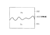
まず、本発明を用いなかった場合における接合メカニズムを説明する。
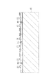
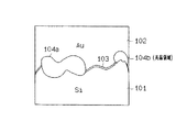
図27に示すように、シリコン101と金薄膜102とを接合する際に、シリコン101および金薄膜102の表面はミクロ的には凹凸を有しており、かつ、シリコン101の表面には自然酸化膜103が形成されている。図28に示すように、シリコン101と金薄膜102とを接触させるとシリコン101の表面と金薄膜102の表面とは点接触した状態となり、さらに金薄膜102に対し加圧力を加えると自然酸化膜103の一部が破れてシリコン101の表面の山(あるいは谷)と金薄膜102の表面の谷(あるいは山)とが嵌め合った状態となる。さらに、共晶温度以上に加熱すると図29に示すようにシリコン101と金薄膜102との界面において共晶領域104a,104bが形成されてシリコン101と金薄膜102とが接合される。このとき、自然酸化膜103の存在によりシリコンと金との接触が妨げられシリコン101と金薄膜102との界面における一部領域にしか共晶領域が形成されない。つまり、前述した加圧力による自然酸化膜103の破れた領域のみが共晶領域となる。
【0012】
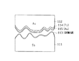
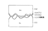
これに対し本発明では以下のメカニズムにより接合する。
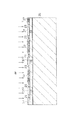
図30に示すように、シリコン111と金薄膜112とを接合する際に、シリコン111および金薄膜112の表面はミクロ的には凹凸を有しており、かつ、シリコン111の表面には自然酸化膜113が形成されている。又、金薄膜112の表面にはチタン薄膜114が形成されている。そして、図31に示すようにシリコン111と金薄膜112とを接触させるとシリコン111の表面と金薄膜112の表面とは点接触した状態となり、さらに、共晶温度以上の加熱開始により図32に示すようにシリコン111と金薄膜112との界面の一部において共晶領域116a,116b,116c,116dが形成され、更なる加熱により図33に示すようにシリコン111と金薄膜112との界面の全域において共晶領域116eが形成される。つまり、チタン薄膜114により自然酸化膜113が還元されシリコンとなり、シリコン111と金薄膜112とが全域において接触した状態となり全域において共晶領域116eが形成される。尚、チタンは酸化されて酸化チタンとなり共晶領域116e内に取り込まれる。
【0013】
このようにしてシリコン111と金薄膜112とが接合される。
よって、金薄膜112の表面に配置したチタン薄膜114の存在により自然酸化膜113によるバリア機能を無くしてシリコンと金とが界面の全領域で接触可能となり、ボイドの発生を抑制して自然酸化膜による接合強度のバラツキを小さくして安定した接合界面を得ることができる。
【0014】
尚、これまでのメカニズムの説明においてはチタン薄膜114を例にとったが、還元性薄膜としてのチタン薄膜の代わりに、シリコン酸化膜に対し還元性のあるアルミ薄膜、タンタル薄膜、ジルコニウム薄膜、ニオブ薄膜であっても同様に機能する。
【0015】
つまり、請求項4のように還元性のある金属薄膜は、チタン薄膜、アルミ薄膜、タンタル薄膜、ジルコニウム薄膜、ニオブ薄膜の内の少なくともいずれか1つを使用するとよい。
【0016】
又、請求項5のように、還元性のある金属薄膜はその厚さを100〜1000Åとすると、最適化が図られる。
又、請求項6のように、還元性のある金属薄膜の表面に金薄膜を形成した後に接合を行うようにしてもよい。つまり、図30においてチタン薄膜114の表面に金薄膜115を設けることによりチタン薄膜114の酸化が防止される。
【0017】
請求項7のように、金薄膜(図30の金薄膜115)はその厚さを200〜500Åとすると、最適化が図られる。
請求項8のように、前記第3工程の接合は真空雰囲気下または不活性ガス雰囲気下または還元雰囲気下で行うと、還元性のある金属薄膜の酸化を抑制でき、酸化防止用の金属膜形成工程を削除することができる。
【0018】
請求項9のように、前記第3工程の接合前においてシリコン部の表面に粗面化処理を施すことにより、シリコン部の表面積を増大させて共晶反応を促進させることができる。この粗面化処理は請求項10のようにスパッタリングまたはアルカリエッチングにて行うことができる。
【0019】
【発明の実施の形態】
以下、この発明を半導体加速度センサに具体化した第1の実施の形態を図面に従って説明する。
【0020】
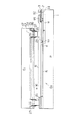
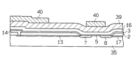
図1は、本実施の形態における可動ゲートMOSトランジスタ型加速度センサの平面図を示す。又、図2には図1のII−II断面を示し、図3には図1のIII −III 断面を示す。
【0021】
第1の基板としてのP型シリコン基板1上にはフィールド酸化膜2が形成されるとともにその上に窒化シリコン膜3が形成されている。
又、P型シリコン基板1上には、フィールド酸化膜2および窒化シリコン膜3の無い長方形状の領域4(図1参照)が形成されている。又、領域4におけるP型シリコン基板1の上にはゲート絶縁膜5が形成されている。窒化シリコン膜3の上には、領域4を架設するように両持ち梁構造の可動ゲート電極6が配置されている。この可動ゲート電極6は帯状にて直線的に延びるポリシリコン薄膜よりなる。又、フィールド酸化膜2および窒化シリコン膜3によりP型シリコン基板1と可動ゲート電極6とが絶縁されている。
【0022】
図3において、P型シリコン基板1上における可動ゲート電極6の両側には不純物拡散層からなる固定ソース電極7と固定ドレイン電極8が形成され、この電極7,8はP型シリコン基板1にイオン注入等によりN型不純物を導入することにより形成されたものである。
【0023】
図2に示すように、P型シリコン基板1にはN型不純物拡散領域9が延設され、N型不純物拡散領域9はアルミ10により可動ゲート電極6と接続されるとともにアルミ配線11と電気的に接続されている。アルミ配線11の他端部はアルミパッド(電極パッド)12として窒化シリコン膜3およびその上に配置されたシリコン酸化膜16から露出している。又、図3に示すように、P型シリコン基板1にはN型不純物拡散領域13が延設され、N型不純物拡散領域13は固定ソース電極7と接続されるとともにアルミ配線14と電気的に接続されている。アルミ配線14の他端部はアルミパッド(電極パッド)15として窒化シリコン膜3およびシリコン酸化膜16から露出している。さらに、P型シリコン基板1にはN型不純物拡散領域17が延設され、N型不純物拡散領域17は固定ドレイン電極8と接続されるとともにアルミ配線18と電気的に接続されている。アルミ配線18の他端部はアルミパッド(電極パッド)19として窒化シリコン膜3およびシリコン酸化膜16から露出している。
【0024】
尚、可動ゲート電極6の形成領域以外の領域はシリコン酸化膜16の上に最終保護膜となる窒化シリコン膜(図示略)が形成される。
そして、アルミパッド12,15,19はボンディングワイヤにて外部の電子回路と接続されている。
【0025】
図3に示すように、P型シリコン基板1における固定ソース電極7と固定ドレイン電極8との間には、反転層20が形成され、同反転層20はシリコン基板1と可動ゲート電極(両持ち梁)6との間に電圧を印加することにより生じたものである。
【0026】
このように本加速度センサは、両持ち梁構造の可動ゲート電極6が配置されており、機械的強度が低い構造となっている。
加速度検出の際には、可動ゲート電極6とシリコン基板1との間に電圧を印加すると、反転層20が形成され、固定ソース電極7と固定ドレイン電極8との間に電流が流れる。そして、本加速度センサが加速度を受けて、図3中に示すZ方向(基板表面に垂直な方向)に可動ゲート電極6が変化した場合には電界強度の変化によって反転層20のキャリア濃度が増大し電流(ドレイン電流)が増大する。このように、本加速度センサは、シリコン基板1の表面に機能素子としてのセンサ素子(可動ゲートMOSトランジスタ)Es が形成され、電流量の増減で加速度を検出することができる。
【0027】
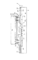
シリコン酸化膜16の上において、センサ素子Es の形成領域の周囲にはポリシリコン薄膜よりなる接合枠(以下、Si接合枠という)21が形成されている。Si接合枠21は帯状をなし、かつ、環状(より詳しくは、四角環状)に配置されている。Si接合枠21の外側におけるSi接合枠21の周辺にアルミパッド(電極パッド)12,15,19が配置されている。
【0028】
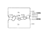
機械的強度の低い可動ゲート電極6を保護するための第2の基板としてのキャップ22は、四角形状のシリコン基板よりなり、このキャップ22の下面に環状の脚部23が設けられている。この脚部23はシリコン基板を局所的にエッチングすることにより形成したものである。キャップ22の下面にはチタン薄膜24、金薄膜25、金薄膜26、チタン薄膜27、金薄膜28が積層されている。より詳しく説明すると、基本構造としてキャップ22の下面にAu/Si共晶接合用の金メッキ薄膜26が形成され、その金メッキ薄膜26の表面がチタン薄膜27(シリコン酸化膜に対し還元性のある金属薄膜)にて覆われ、チタン薄膜27は酸化保護用の金薄膜28にて覆われ、金メッキ薄膜26とキャップ22との間にはチタン薄膜24およびメッキ下地用金薄膜25が介在されている。
【0029】
ここで、金薄膜(メッキによる膜)26の膜厚は3.5μmであり、チタン薄膜24および金薄膜25の膜厚は1000Åである。又、チタン薄膜27の膜厚は50〜800Åであり、金薄膜28は200Åである。
【0030】
キャップ22側の脚部23の先端面(下面)とP型シリコン基板1側のSi接合枠21とは、Au/Si共晶体29にて接合されている。より詳しくは、Si接合枠(ポリシリコン薄膜)21と金薄膜26とをAu/Si共晶温度の363℃以上に加熱することにより共晶反応を起こさせてAu/Si共晶体29にて接合している。このAu/Si共晶体29は脚部23の先端面(下面)の全面において形成され、ボイドレスな接合となっている。つまり、チタン薄膜27からのチタン(シリコン酸化物を還元する金属)によりSi接合枠21表面の自然酸化膜が還元され、このときのチタンの酸化物がAu/Si共晶体29内に存在する。尚、Au/Si共晶体29は、図26のAu−Siの相図に示すように、Siが3.1wt%の組成比となる。
【0031】
このように、Si接合枠21に対してキャップ22を接合することにより、シリコン基板1の表面においてキャップ22内の空隙30にセンサ素子(可動ゲートMOSトランジスタ)Es が封止された構造となっている。即ち、センサ素子Es が形成されたシリコン基板1に対しキャップ22が空隙30をもって対向配置され、この空隙30にセンサ素子Es が封止された構造をなし、このキャップ22にてウェハからチップにダイシングカットする際の水圧や水流から可動ゲート電極6(振動部)を保護することができる。又、保護キャップ22によりセンサ素子(可動ゲートMOSトランジスタ)Es が気密封止された状態で保護されている。
【0032】
次に、キャップ22による封止構造の形成工程を、図4〜図17に基づいて説明する。
尚、この工程は量産性を考慮してキャップとなるチップを一個一個センサチップに接合するのではなくキャップを一括で接合している。
【0033】
まず、図4に示すように、キャップとなる第2の基板としてのシリコンウェハ(以下、キャップ形成用ウェハと呼ぶ)31を用意する。キャップ形成用ウェハ31はセンサ素子形成用シリコンウェハと同サイズのものを用いる。そして、キャップ形成用ウェハ31の主表面に熱酸化膜32を5000Å形成するとともに裏面にも熱酸化膜33を5000Å形成する。さらに、キャップ形成用ウェハ31の主表面側の熱酸化膜32をホトエッチングにより所望の形状にパターニングする。
【0034】
その後、図5に示すように、熱酸化膜32をマスクとしてキャップ形成用ウェハ31をエッチングして凹部34を形成する。この際、エッチング液はKOHなどのアルカリ性溶液を用い、異方性エッチングにより凹部34を形成する。つまり、キャップ材として(100)面のシリコンウェハ31を用いる場合において、シリコン酸化膜32をパターニングマスクとしアルカリ性エッチング液を用いた異方性エッチングにより凹部34を形成する。その結果、キャップ形成用ウェハ31の主表面において凹部34間にSi脚部(凸部)23が形成され、このSi脚部23は接合枠パターンに対応する。このSi脚部(凸部)23は、後の工程でキャップ形成用ウェハ31をダイシングカットする際に、ダイシングブレードとセンサ素子形成用シリコンウェハとの接触を回避するための必要な間隙を確保するためのものである。
【0035】
さらに、図6に示すように、マスクとした熱酸化膜32及び裏面の酸化膜33をHF等により除去する。
引き続き、図7に示すように、キャップ形成用ウェハ31の主表面にチタン薄膜24および金薄膜25を蒸着法あるいはスパッタリング法により真空中で連続的に成膜する。このとき、チタン薄膜24および金薄膜25の膜厚は1000Åとする。尚、チタン薄膜24は金薄膜25とキャップ側シリコン21との密着性を良好なものとするためのものである。金薄膜25は次工程での金メッキ膜26のシードとして用いているがこの金薄膜25は省略してもよい。
【0036】
そして、図8に示すように、金薄膜25の表面に金薄膜26を電解メッキ法により全面メッキする。金薄膜26の膜厚は3.5μmとする。
さらに、図9に示すように、金薄膜26の表面にボイドレス接合とするためのチタン薄膜27とその酸化防止のための金薄膜28を真空中で連続的に成膜する。このときのチタン薄膜27の膜厚は50〜800Åとする。これは、1000Å以上となると酸化チタンの他にTiシリサイドが多量に形成され接合強度が低下してくるためである。又、金薄膜28の膜厚は金薄膜28中のTiがシリコン表面へ拡散することを考慮して200Åとする。
【0037】
一方、図10に示すように、センサ素子Es の形成のための第1の基板としてのシリコンウェハ(以下、素子形成用ウェハと呼ぶ)35を用意する。この素子形成用ウェハ35には、犠牲層エッチングにより梁構造体を形成する前の可動ゲート電極6が形成されるとともに、ポリシリコン薄膜よりなるSi接合枠21が形成されている。そして、Si接合枠21(素子形成用ウェハの接合部)の表面を粗面化する。具体的にはアルゴン(Ar)をSi接合枠21に照射してその表面をスパッタリングする。つまり、図11に示すように、Si接合枠21(接合領域)のみが開口するように素子形成用ウェハ35の主表面にレジスト37を塗布し、アルゴン(Ar)によりSi接合枠(ポリシリコン薄膜)21の表面を僅かにスパッタリングする。
【0038】
さらに、レジスト37を剥離した後、図12に示すように、可動ゲート電極6の回りの犠牲層をエッチングにて除去し、梁構造体を形成する。
ここで、図10〜図12により説明した工程の詳細を、図18〜図22を用いて説明する。
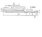
【0039】
まず、図18に示すように、シリコン基板1となる素子形成用ウェハ35にフィールド酸化膜2およびゲート絶縁膜5、不純物拡散層(固定ソース電極7、固定ドレイン電極8、拡散領域9,13,17)、引き出し用アルミ配線14等を形成し、さらにエッチングストッパとなる窒化シリコン膜3をパターニングする。その上に犠牲層となるシリコン酸化膜16を形成し、所望の形状にパターニングする。そして、その上に可動ゲート電極およびSi接合枠となるポリシリコン薄膜39を堆積するとともにホトレジスト40を配置する。
【0040】
さらに、図19に示すように、ポリシリコン薄膜39を通常のホトリソ工程によりパターニングして可動ゲート電極形成領域にポリシリコン薄膜39aを配置するとともにSi接合枠の形成領域(ウェハの表面におけるセンサ素子の形成領域の周囲)にポリシリコン薄膜39bを配置する。
【0041】
引き続き、図20に示すように、素子形成用ウェハ35の上にICチップの最終保護膜となる絶縁膜41(例えばプラズマCVD法による窒素シリコン膜)を形成し、可動ゲート電極形成領域の周辺およびSi接合枠形成領域を保護するようにパターニングする。さらに、絶縁膜41の上にホトレジスト42を形成する。そして、図21に示すように、ホトレジスト42を用いて絶縁膜41を窓開けする
さらに、図22に示すように、ホトレジスト43を用いてフッ酸系のエッチング液でシリコン酸化膜16の犠牲層エッチングを行い、ポリシリコン薄膜39aの周囲のシリコン酸化膜16のみをエッチングする。これにより、可動ゲート電極6の周囲に空隙が確保される。最後に、ホトレジスト43を除去して可動ゲート電極6の形成およびSi接合枠21の形成工程が完了する。
【0042】
図18〜図22(図10〜図12)の工程が終了すると、次に、素子形成用ウェハ35へのキャップ形成用ウェハ31の接合およびウェハダイシングカットを行う。
【0043】
まず、図13に示すように、脚部23を形成したキャップ形成用ウェハ31を、センサ素子Es が形成されている素子形成用ウェハ35に位置合わせして、Si接合枠21と脚部23に形成された薄膜積層部24〜28(Au膜)を重ね合わせる。より具体的には、図23に示すように、オリエンテーションフラット面を基準にしてキャップ形成用ウェハ31と素子形成用ウェハ35とを位置合わせしてキャップ形成用ウェハ31を素子形成用ウェハ35にマウントする。このオリエンテーションフラット面に平行なるX方向が第1のダイシングカットラインとなるとともに、オリエンテーションフラット面に垂直なるY方向が第2のダイシングカットラインとなる。さらに、図13のキャップ形成用ウェハ31と素子形成用ウェハ35とを、チタン薄膜27が酸化しないように真空中あるいはN2 等の不活性ガス中あるいは還元雰囲気中で、400℃にて10分間ホールドし、その後、冷却することで接合する。加圧力は0.8kgf/mm2 とする。
【0044】
つまり、Si接合枠(ポリシリコン薄膜)21と金薄膜26とをAu/Si共晶温度の363℃以上に加熱することにより共晶反応を起こさせてAu/Si共晶体29にて接合する。その接合のメカニズムについては図30〜図33を用いて説明した通りであり、ここではその説明は省くが、チタン薄膜27からのチタン(シリコン酸化物を還元する金属)により脚部23の先端面(下面)の全面においてAu/Si共晶体29が形成され、このAu/Si共晶体29にはシリコン表面の自然酸化膜の還元に伴うチタンの酸化物を含有している。
【0045】
このようにチップ化する前のキャップ形成用ウェハ31を一括接合した後、図14に示すようにキャップ形成用ウェハ31をダイシングカットし、キャップ形成用ウェハ31に対し切断しキャップ部45aとキャップ不要部45bとを分離する。つまり、ダイシングカットにより、図23のオリエンテーションフラット面に対して垂直方向(図中、Y方向)に図14の切れ込み46が入る。
【0046】
そして、図15に示すように、粘着シート47をキャップ形成用ウェハ31の裏面に貼り付け、粘着シート47ごと再度ダイシングカットする。このダイシングカットにより、図23のオリエンテーションフラット面に対して水平方向(図中、X方向)に図15の切れ込み48が入る。
【0047】
引き続き、図16に示すように、分割されたキャップ形成用ウェハ31から粘着シート47を剥がす。このとき、粘着シート47とともにキャップ不要部45bはすべて除去され、素子形成用ウェハ35上にキャップ22が搭載された形となる。
【0048】
キャップ形成用ウェハ31の切断および不要部除去工程が終了すると、次に図17に示すように、素子形成用ウェハ35に対しダイシングカット位置49でのタイシングラインに沿ったダイシングカットを行う。その結果、図1〜図3のように個々のセンサチップに分割される。このダイシングの際に水流や水圧が加わるが、外力から保護する必要のある機能素子(梁構造を有するセンサ素子等)がキャップ22により保護される。
【0049】
このようにして、図1〜図3に示す半導体加速度センサが製造される。
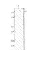
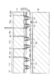
図24には、図2のチタン薄膜27の膜厚に対する接合強度の測定結果を示す。この図24においてチタン薄膜27の膜厚が「0」のとき、即ち、チタン薄膜27が無いときには接合強度は6.3MPa〜17.3MPaの範囲となり、そのバラツキΔL1は11.0MPaとなる。又、チタン薄膜27の膜厚が4nmのときには接合強度は4.6MPa〜9.7MPaの範囲となり、そのバラツキは5.1MPaとなる。同様に、チタン薄膜27の膜厚が10nmのときには接合強度は6.4MPa〜12.2MPaの範囲となり、そのバラツキは5.8MPaとなる。チタン薄膜27の膜厚が20nmのときには接合強度は4.8MPa〜12.0MPaの範囲となり、そのバラツキは7.2MPaとなる。チタン薄膜27の膜厚が40nmのときには接合強度は5.6MPa〜10.7MPaの範囲となり、そのバラツキは5.1MPaとなる。チタン薄膜27の膜厚が56nmのときには接合強度は10.0MPa〜14.1MPaの範囲となり、そのバラツキΔL2は4.1MPaとなる。チタン薄膜27の膜厚が150nmのときには接合強度は2.4MPa〜11.1MPaの範囲となり、そのバラツキは8.7MPaとなる。
【0050】
この結果から、シリコン酸化膜に対し還元性のある金属薄膜としてのチタン薄膜27はその厚さを100〜1000Å(10〜100nm)とすると、接合強度のバラツキを小さくすることができることが分かる。
【0051】
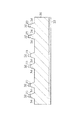
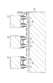
図25には、図2の金薄膜28の膜厚に対する反応面積比率の測定結果を示す。つまり、横軸に図2のチタン薄膜27の膜厚をとり、縦軸に反応面積比率(全接触面積のうちの共晶反応が起こっている面積比)をとり、金薄膜28の厚さとして「0」の場合、20nmの場合、100nmの場合でプロットしている。尚、図25中にはプロットしていないが、金薄膜28の厚さが50nmの場合には20nmの場合とほぼ同じ値をとった。
【0052】
この図25から金薄膜28の厚さとして20nmとした場合が最も反応面積比率が高くなり、次に反応面積比率が高いのは金薄膜28の厚さが100nmの場合であり、金薄膜28の厚さとして「0」の場合が反応面積比率が最も低くなった。
【0053】
この結果から、チタン薄膜27の表面に設けられ、チタン薄膜27の酸化防止のための金薄膜28は、その厚さを200〜500Å(20〜50nm)とするとよいことが分かった。
【0054】
このように本実施の形態は、下記の特徴を有する。
(イ)半導体装置の製造方法として、図8のようにキャップ形成用ウェハ31での、素子形成用ウェハ35の表面における少なくともセンサ素子Es の形成領域の周囲に対応する部位に金の薄膜26を形成し(第1工程)、図9のように金の薄膜26の表面に、シリコン酸化膜に対し還元性のあるチタン薄膜27を形成し(第2工程)、図13のようにキャップ形成用ウェハ31の金薄膜26と素子形成用ウェハ35のシリコン部とを接近させた状態から、Au/Si共晶温度以上に加熱して素子形成用ウェハ35のSi接合枠21(シリコン部)とキャップ形成用ウェハ31の金の薄膜26とを接合し(第3工程)、図17のように素子形成用ウェハ35を各チップ毎にダイシングして各チップに裁断した(第3工程)。
【0055】
その結果、Si接合枠21(シリコン部)の表面には自然酸化膜が形成されるが、還元性のあるチタン薄膜27の存在によりこの自然酸化膜による接合強度のバラツキを小さくして(図24のΔL2<ΔL1)、安定した接合界面を得ることができ、半導体装置を高歩留りで製造することができる。ここで、Au/Si共晶体29にはチタンによるシリコン酸化膜の還元に伴うチタンの酸化物が残る。
(ロ)図24のように還元性のあるチタン薄膜27はその厚さを100〜1000Åとすると、最適化が図られる。
(ハ)還元性のあるチタン薄膜27の表面に金薄膜28を形成した後にウェハ接合を行うと、チタン薄膜27の酸化が防止できる。
(ニ)図25のように金薄膜28はその厚さを200〜500Åとすると、最適化が図られる。
(ホ)ウェハ接合は真空雰囲気下または不活性ガス雰囲気下または還元雰囲気下で行うと、チタン薄膜27の酸化を抑制できる。
(ヘ)図11のようにウェハ接合前においてスパッタリングによりSi接合枠21の表面に粗面化処理を施すことにより、シリコン部の表面積を増大させて共晶反応を促進させることができる。
【0056】
これまで述べてきた実施の形態以外にも下記のように実施してもよい。
上記の実施の形態ではボイドレスな接合を達成するためにチタン薄膜27を用いているが、他のシリコン酸化膜を還元する金属であるAl(アルミ)、Ta(タンタル)、Zr(ジルコニウム)、Nb(ニオブ)の薄膜を用いてもよい。この場合も接合時の雰囲気は不活性ガス、還元性ガス、あるいは真空中で行うとよい。
【0057】
又、シリコンの接合前の表面処理(粗面化処理)は、Ar(アルゴン)によるスパッタリングの他にも、シリコンエッチング液(アルカリ性溶液)による処理にて行ってもよい。
【0058】
さらに、カットするウェハの順序は、センサ形成用ウェハ35からカットし、最後にキャップ形成用ウェハ31をカットしてもよい。
さらには、Si接合枠21として、ポリシリコン薄膜の代わりに、単結晶シリコン薄膜や非晶質シリコン薄膜を用いたり、バルクの単結晶シリコンを用いてもよい。ここで、接合用シリコンとして単結晶シリコンを用いた場合に、表面の粗面化処理を施すことの効果が大きい。
【0059】
又、キャップ形成用ウェハのウェハ材料は、シリコンの他に、ガラス、セラミクス、樹脂等を用いることができる。
さらに、半導体加速度センサの他にも、マイクロダイヤフラム圧力センサやヨーレイトセンサなどシリコンチップ上に可動部(振動部)を有する半導体装置に具体化したり、さらに、接触子等を備えた装置に具体化できる。さらに、表面実装における接合技術(フリップチップボンディング等)にも適用できる。
【図面の簡単な説明】
【図1】実施の形態の半導体装置の平面図。
【図2】図1のII−II断面図。
【図3】図1のIII −III 断面図。
【図4】実施の形態の半導体装置の製造工程を示す断面図。
【図5】実施の形態の半導体装置の製造工程を示す断面図。
【図6】実施の形態の半導体装置の製造工程を示す断面図。
【図7】実施の形態の半導体装置の製造工程を示す断面図。
【図8】実施の形態の半導体装置の製造工程を示す断面図。
【図9】実施の形態の半導体装置の製造工程を示す断面図。
【図10】実施の形態の半導体装置の製造工程を示す断面図。
【図11】実施の形態の半導体装置の製造工程を示す断面図。
【図12】実施の形態の半導体装置の製造工程を示す断面図。
【図13】実施の形態の半導体装置の製造工程を示す断面図。
【図14】実施の形態の半導体装置の製造工程を示す平面図。
【図15】実施の形態の半導体装置の製造工程を示す平面図。
【図16】実施の形態の半導体装置の製造工程を示す平面図。
【図17】実施の形態の半導体装置の製造工程を示す断面図。
【図18】実施の形態の半導体装置の製造工程を示す断面図。
【図19】実施の形態の半導体装置の製造工程を示す断面図。
【図20】実施の形態の半導体装置の製造工程を示す断面図。
【図21】実施の形態の半導体装置の製造工程を示す断面図。
【図22】実施の形態の半導体装置の製造工程を示す断面図。
【図23】実施の形態の半導体装置の製造工程を示す平面図。
【図24】接合強度の測定結果を示す図。
【図25】反応面積比の測定結果を示す図。
【図26】相状態を示す状態図。
【図27】接合原理を説明するための断面図。
【図28】接合原理を説明するための断面図。
【図29】接合原理を説明するための断面図。
【図30】接合原理を説明するための断面図。
【図31】接合原理を説明するための断面図。
【図32】接合原理を説明するための断面図。
【図33】接合原理を説明するための断面図。
【符号の説明】
1…第1の基板としてのシリコン基板、6…可動ゲート電極、7…固定ソース電極、8…固定ドレイン電極、21…Si接合枠、22…第2の基板としてのキャップ、26…金薄膜、27…チタン薄膜、28…金薄膜、29…Au/Si共結晶体、30…空隙、31…第2の基板としてのキャップ形成用ウェハ、35…第1の基板としての素子形成用ウェハ、Es …機能素子としてのセンサ素子。
Claims (10)
- シリコン部を有する第1の基板と、金薄膜と該金薄膜の表面に形成されてシリコン酸化膜に対し還元性のある金属薄膜とからなる接合部を有する第2の基板とが対向配置され、両基板が、前記シリコン部と前記接合部の金薄膜とのAu/Si共晶体にて接合された半導体装置において、
前記Au/Si共晶体の内部には、前記シリコン部表面の自然酸化膜であるシリコン酸化膜に対し還元性のある金属薄膜の酸化物が含有されてなる半導体装置。 - 表面にシリコン酸化膜が形成されたシリコン部を有する第1の基板に第2の基板が対向した状態で接合される半導体装置の製造方法であって、
第2の基板における少なくとも接合部に金の薄膜を形成する第1工程と、
前記金の薄膜の表面に、前記シリコン酸化膜に対し還元性のある金属薄膜を形成する第2工程と、
前記第2の基板の金属薄膜と第1の基板のシリコン部とを接近させた状態から、Au/Si共晶温度以上に加熱して前記第1の基板のシリコン部と前記第2の基板の金の薄膜とを接合する第3工程と、
前記第1の基板を各チップ毎にダイシングする第4工程と
を備えたことを特徴とする半導体装置の製造方法。 - 表面にシリコン酸化膜が形成されたシリコン部を有する第1の基板の表面に機能素子が形成されるとともに、該第1の基板の表面において機能素子に対し空隙をもって覆うキャップが設けられた半導体装置の製造方法であって、
キャップ形成用の第2の基板での、第1の基板の表面における少なくとも機能素子の形成領域の周囲に対応する部位に金の薄膜を形成する第1工程と、
前記金の薄膜の表面に、シリコン酸化膜に対し還元性のある金属薄膜を形成する第2工程と、
前記第2の基板の金属薄膜と第1の基板のシリコン部とを接近させた状態から、Au/Si共晶温度以上に加熱して前記第1の基板のシリコン部と前記第2の基板の金の薄膜とを接合する第3工程と、
前記第1の基板を各チップ毎にダイシングする第4工程と
を備えたことを特徴とする半導体装置の製造方法。 - 還元性のある金属薄膜は、チタン薄膜、アルミ薄膜、タンタル薄膜、ジルコニウム薄膜、ニオブ薄膜の内の少なくともいずれか1つである請求項2に記載の半導体装置の製造方法。
- 還元性のある金属薄膜はその厚さが100〜1000Åである請求項2に記載の半導体装置の製造方法。
- 還元性のある金属薄膜の表面に金薄膜を形成した後に接合を行うようにした請求項2に記載の半導体装置の製造方法。
- 前記金薄膜はその厚さが200〜500Åである請求項6に記載の半導体装置の製造方法。
- 前記第3工程の接合は真空雰囲気下または不活性ガス雰囲気下または還元雰囲気下で行うものである請求項2に記載の半導体装置の製造方法。
- 前記第3工程の接合前においてシリコン部の表面に粗面化処理を行うようにした請求項2に記載の半導体装置の製造方法。
- 粗面化処理はスパッタリングまたはアルカリエッチングにより行うようにした請求項9に記載の半導体装置の製造方法。
Priority Applications (2)
| Application Number | Priority Date | Filing Date | Title |
|---|---|---|---|
| JP26464296A JP3584635B2 (ja) | 1996-10-04 | 1996-10-04 | 半導体装置及びその製造方法 |
| US08/943,146 US6555901B1 (en) | 1996-10-04 | 1997-10-03 | Semiconductor device including eutectic bonding portion and method for manufacturing the same |
Applications Claiming Priority (1)
| Application Number | Priority Date | Filing Date | Title |
|---|---|---|---|
| JP26464296A JP3584635B2 (ja) | 1996-10-04 | 1996-10-04 | 半導体装置及びその製造方法 |
Publications (2)
| Publication Number | Publication Date |
|---|---|
| JPH10112548A JPH10112548A (ja) | 1998-04-28 |
| JP3584635B2 true JP3584635B2 (ja) | 2004-11-04 |
Family
ID=17406197
Family Applications (1)
| Application Number | Title | Priority Date | Filing Date |
|---|---|---|---|
| JP26464296A Expired - Fee Related JP3584635B2 (ja) | 1996-10-04 | 1996-10-04 | 半導体装置及びその製造方法 |
Country Status (2)
| Country | Link |
|---|---|
| US (1) | US6555901B1 (ja) |
| JP (1) | JP3584635B2 (ja) |
Families Citing this family (273)
| Publication number | Priority date | Publication date | Assignee | Title |
|---|---|---|---|---|
| US20050280155A1 (en) * | 2004-06-21 | 2005-12-22 | Sang-Yun Lee | Semiconductor bonding and layer transfer method |
| US8058142B2 (en) * | 1996-11-04 | 2011-11-15 | Besang Inc. | Bonded semiconductor structure and method of making the same |
| US8018058B2 (en) * | 2004-06-21 | 2011-09-13 | Besang Inc. | Semiconductor memory device |
| AUPR244801A0 (en) * | 2001-01-10 | 2001-02-01 | Silverbrook Research Pty Ltd | A method and apparatus (WSM01) |
| US6856007B2 (en) * | 2001-08-28 | 2005-02-15 | Tessera, Inc. | High-frequency chip packages |
| FR2834283B1 (fr) * | 2001-12-28 | 2005-06-24 | Commissariat Energie Atomique | Procede et zone de scellement entre deux substrats d'une microstructure |
| US6955976B2 (en) * | 2002-02-01 | 2005-10-18 | Hewlett-Packard Development Company, L.P. | Method for dicing wafer stacks to provide access to interior structures |
| DE10232190A1 (de) * | 2002-07-16 | 2004-02-05 | Austriamicrosystems Ag | Verfahren zur Herstellung eines Bauelements mit tiefliegenden Anschlußflächen |
| US20100133695A1 (en) * | 2003-01-12 | 2010-06-03 | Sang-Yun Lee | Electronic circuit with embedded memory |
| US7754537B2 (en) * | 2003-02-25 | 2010-07-13 | Tessera, Inc. | Manufacture of mountable capped chips |
| US7514283B2 (en) * | 2003-03-20 | 2009-04-07 | Robert Bosch Gmbh | Method of fabricating electromechanical device having a controlled atmosphere |
| US8912174B2 (en) * | 2003-04-16 | 2014-12-16 | Mylan Pharmaceuticals Inc. | Formulations and methods for treating rhinosinusitis |
| US6936491B2 (en) | 2003-06-04 | 2005-08-30 | Robert Bosch Gmbh | Method of fabricating microelectromechanical systems and devices having trench isolated contacts |
| US7075160B2 (en) | 2003-06-04 | 2006-07-11 | Robert Bosch Gmbh | Microelectromechanical systems and devices having thin film encapsulated mechanical structures |
| US6972480B2 (en) | 2003-06-16 | 2005-12-06 | Shellcase Ltd. | Methods and apparatus for packaging integrated circuit devices |
| US8071438B2 (en) * | 2003-06-24 | 2011-12-06 | Besang Inc. | Semiconductor circuit |
| US20100190334A1 (en) * | 2003-06-24 | 2010-07-29 | Sang-Yun Lee | Three-dimensional semiconductor structure and method of manufacturing the same |
| WO2005004195A2 (en) * | 2003-07-03 | 2005-01-13 | Shellcase Ltd. | Method and apparatus for packaging integrated circuit devices |
| US6952041B2 (en) * | 2003-07-25 | 2005-10-04 | Robert Bosch Gmbh | Anchors for microelectromechanical systems having an SOI substrate, and method of fabricating same |
| US7224056B2 (en) * | 2003-09-26 | 2007-05-29 | Tessera, Inc. | Back-face and edge interconnects for lidded package |
| WO2005086532A2 (en) * | 2004-03-01 | 2005-09-15 | Tessera, Inc. | Packaged acoustic and electromagnetic transducer chips |
| US7068125B2 (en) | 2004-03-04 | 2006-06-27 | Robert Bosch Gmbh | Temperature controlled MEMS resonator and method for controlling resonator frequency |
| US7102467B2 (en) * | 2004-04-28 | 2006-09-05 | Robert Bosch Gmbh | Method for adjusting the frequency of a MEMS resonator |
| US7078320B2 (en) * | 2004-08-10 | 2006-07-18 | International Business Machines Corporation | Partial wafer bonding and dicing |
| DE102004058880B4 (de) * | 2004-12-06 | 2007-12-13 | Austriamicrosystems Ag | Integrierter Mikrosensor und Verfahren zur Herstellung |
| FR2879183B1 (fr) * | 2004-12-15 | 2007-04-27 | Atmel Grenoble Soc Par Actions | Procede de fabrication collective de microstructures a elements superposes |
| US8143095B2 (en) * | 2005-03-22 | 2012-03-27 | Tessera, Inc. | Sequential fabrication of vertical conductive interconnects in capped chips |
| US20110143506A1 (en) * | 2009-12-10 | 2011-06-16 | Sang-Yun Lee | Method for fabricating a semiconductor memory device |
| US8367524B2 (en) * | 2005-03-29 | 2013-02-05 | Sang-Yun Lee | Three-dimensional integrated circuit structure |
| JP2007027279A (ja) * | 2005-07-13 | 2007-02-01 | Shinko Electric Ind Co Ltd | 半導体装置および半導体装置の製造方法 |
| CN101317263B (zh) * | 2005-11-25 | 2012-03-21 | 松下电工株式会社 | 传感器装置及其制造方法 |
| WO2007061047A1 (ja) * | 2005-11-25 | 2007-05-31 | Matsushita Electric Works, Ltd. | ウェハレベルパッケージ構造体およびその製造方法 |
| US8067769B2 (en) * | 2005-11-25 | 2011-11-29 | Panasonic Electric Works Co., Ltd. | Wafer level package structure, and sensor device obtained from the same package structure |
| KR100985453B1 (ko) * | 2005-11-25 | 2010-10-05 | 파나소닉 전공 주식회사 | 센서 장치 및 그 제조 방법 |
| US20070170528A1 (en) | 2006-01-20 | 2007-07-26 | Aaron Partridge | Wafer encapsulated microelectromechanical structure and method of manufacturing same |
| US7936062B2 (en) * | 2006-01-23 | 2011-05-03 | Tessera Technologies Ireland Limited | Wafer level chip packaging |
| US20070190747A1 (en) * | 2006-01-23 | 2007-08-16 | Tessera Technologies Hungary Kft. | Wafer level packaging to lidded chips |
| US7402899B1 (en) | 2006-02-03 | 2008-07-22 | Pacesetter, Inc. | Hermetically sealable silicon system and method of making same |
| US20080002460A1 (en) * | 2006-03-01 | 2008-01-03 | Tessera, Inc. | Structure and method of making lidded chips |
| US8604605B2 (en) * | 2007-01-05 | 2013-12-10 | Invensas Corp. | Microelectronic assembly with multi-layer support structure |
| US8716850B2 (en) * | 2007-05-18 | 2014-05-06 | Semiconductor Energy Laboratory Co., Ltd. | Semiconductor device and method for manufacturing the same |
| KR100908648B1 (ko) * | 2007-10-19 | 2009-07-21 | (주)에스엠엘전자 | 복층 범프 구조물 및 그 제조 방법 |
| JP4915677B2 (ja) * | 2008-05-27 | 2012-04-11 | パナソニック株式会社 | センサ装置の製造方法 |
| JP5442277B2 (ja) * | 2008-09-22 | 2014-03-12 | アルプス電気株式会社 | Memsセンサ及びその製造方法 |
| JP4924663B2 (ja) * | 2008-12-25 | 2012-04-25 | 株式会社デンソー | 半導体装置およびその製造方法 |
| US8343806B2 (en) | 2009-03-05 | 2013-01-01 | Raytheon Company | Hermetic packaging of integrated circuit components |
| US8362800B2 (en) | 2010-10-13 | 2013-01-29 | Monolithic 3D Inc. | 3D semiconductor device including field repairable logics |
| US8405420B2 (en) | 2009-04-14 | 2013-03-26 | Monolithic 3D Inc. | System comprising a semiconductor device and structure |
| US8378715B2 (en) | 2009-04-14 | 2013-02-19 | Monolithic 3D Inc. | Method to construct systems |
| US8754533B2 (en) | 2009-04-14 | 2014-06-17 | Monolithic 3D Inc. | Monolithic three-dimensional semiconductor device and structure |
| US8362482B2 (en) | 2009-04-14 | 2013-01-29 | Monolithic 3D Inc. | Semiconductor device and structure |
| US8395191B2 (en) | 2009-10-12 | 2013-03-12 | Monolithic 3D Inc. | Semiconductor device and structure |
| US7986042B2 (en) | 2009-04-14 | 2011-07-26 | Monolithic 3D Inc. | Method for fabrication of a semiconductor device and structure |
| US8669778B1 (en) | 2009-04-14 | 2014-03-11 | Monolithic 3D Inc. | Method for design and manufacturing of a 3D semiconductor device |
| US8058137B1 (en) | 2009-04-14 | 2011-11-15 | Monolithic 3D Inc. | Method for fabrication of a semiconductor device and structure |
| US8427200B2 (en) | 2009-04-14 | 2013-04-23 | Monolithic 3D Inc. | 3D semiconductor device |
| US9509313B2 (en) | 2009-04-14 | 2016-11-29 | Monolithic 3D Inc. | 3D semiconductor device |
| US8373439B2 (en) | 2009-04-14 | 2013-02-12 | Monolithic 3D Inc. | 3D semiconductor device |
| US9711407B2 (en) | 2009-04-14 | 2017-07-18 | Monolithic 3D Inc. | Method of manufacturing a three dimensional integrated circuit by transfer of a mono-crystalline layer |
| US9577642B2 (en) | 2009-04-14 | 2017-02-21 | Monolithic 3D Inc. | Method to form a 3D semiconductor device |
| US8384426B2 (en) * | 2009-04-14 | 2013-02-26 | Monolithic 3D Inc. | Semiconductor device and structure |
| US8742476B1 (en) | 2012-11-27 | 2014-06-03 | Monolithic 3D Inc. | Semiconductor device and structure |
| US8536023B2 (en) | 2010-11-22 | 2013-09-17 | Monolithic 3D Inc. | Method of manufacturing a semiconductor device and structure |
| US10354995B2 (en) | 2009-10-12 | 2019-07-16 | Monolithic 3D Inc. | Semiconductor memory device and structure |
| US11018133B2 (en) | 2009-10-12 | 2021-05-25 | Monolithic 3D Inc. | 3D integrated circuit |
| US10043781B2 (en) | 2009-10-12 | 2018-08-07 | Monolithic 3D Inc. | 3D semiconductor device and structure |
| US8450804B2 (en) | 2011-03-06 | 2013-05-28 | Monolithic 3D Inc. | Semiconductor device and structure for heat removal |
| US11374118B2 (en) | 2009-10-12 | 2022-06-28 | Monolithic 3D Inc. | Method to form a 3D integrated circuit |
| US8148728B2 (en) | 2009-10-12 | 2012-04-03 | Monolithic 3D, Inc. | Method for fabrication of a semiconductor device and structure |
| US10366970B2 (en) | 2009-10-12 | 2019-07-30 | Monolithic 3D Inc. | 3D semiconductor device and structure |
| US10910364B2 (en) | 2009-10-12 | 2021-02-02 | Monolitaic 3D Inc. | 3D semiconductor device |
| US10388863B2 (en) | 2009-10-12 | 2019-08-20 | Monolithic 3D Inc. | 3D memory device and structure |
| US10157909B2 (en) | 2009-10-12 | 2018-12-18 | Monolithic 3D Inc. | 3D semiconductor device and structure |
| US8581349B1 (en) | 2011-05-02 | 2013-11-12 | Monolithic 3D Inc. | 3D memory semiconductor device and structure |
| US11984445B2 (en) | 2009-10-12 | 2024-05-14 | Monolithic 3D Inc. | 3D semiconductor devices and structures with metal layers |
| US8476145B2 (en) | 2010-10-13 | 2013-07-02 | Monolithic 3D Inc. | Method of fabricating a semiconductor device and structure |
| US9099424B1 (en) | 2012-08-10 | 2015-08-04 | Monolithic 3D Inc. | Semiconductor system, device and structure with heat removal |
| US12027518B1 (en) | 2009-10-12 | 2024-07-02 | Monolithic 3D Inc. | 3D semiconductor devices and structures with metal layers |
| US8492886B2 (en) | 2010-02-16 | 2013-07-23 | Monolithic 3D Inc | 3D integrated circuit with logic |
| US8541819B1 (en) | 2010-12-09 | 2013-09-24 | Monolithic 3D Inc. | Semiconductor device and structure |
| US9099526B2 (en) | 2010-02-16 | 2015-08-04 | Monolithic 3D Inc. | Integrated circuit device and structure |
| US8026521B1 (en) | 2010-10-11 | 2011-09-27 | Monolithic 3D Inc. | Semiconductor device and structure |
| US8461035B1 (en) | 2010-09-30 | 2013-06-11 | Monolithic 3D Inc. | Method for fabrication of a semiconductor device and structure |
| US8373230B1 (en) | 2010-10-13 | 2013-02-12 | Monolithic 3D Inc. | Method for fabrication of a semiconductor device and structure |
| KR101134819B1 (ko) | 2010-07-02 | 2012-04-13 | 이상윤 | 반도체 메모리 장치의 제조 방법 |
| US9953925B2 (en) | 2011-06-28 | 2018-04-24 | Monolithic 3D Inc. | Semiconductor system and device |
| US9219005B2 (en) | 2011-06-28 | 2015-12-22 | Monolithic 3D Inc. | Semiconductor system and device |
| US8901613B2 (en) | 2011-03-06 | 2014-12-02 | Monolithic 3D Inc. | Semiconductor device and structure for heat removal |
| US8642416B2 (en) | 2010-07-30 | 2014-02-04 | Monolithic 3D Inc. | Method of forming three dimensional integrated circuit devices using layer transfer technique |
| US10217667B2 (en) | 2011-06-28 | 2019-02-26 | Monolithic 3D Inc. | 3D semiconductor device, fabrication method and system |
| US8163581B1 (en) | 2010-10-13 | 2012-04-24 | Monolith IC 3D | Semiconductor and optoelectronic devices |
| US12362219B2 (en) | 2010-11-18 | 2025-07-15 | Monolithic 3D Inc. | 3D semiconductor memory device and structure |
| US10497713B2 (en) | 2010-11-18 | 2019-12-03 | Monolithic 3D Inc. | 3D semiconductor memory device and structure |
| US8273610B2 (en) | 2010-11-18 | 2012-09-25 | Monolithic 3D Inc. | Method of constructing a semiconductor device and structure |
| US11482440B2 (en) | 2010-12-16 | 2022-10-25 | Monolithic 3D Inc. | 3D semiconductor device and structure with a built-in test circuit for repairing faulty circuits |
| US11257867B1 (en) | 2010-10-11 | 2022-02-22 | Monolithic 3D Inc. | 3D semiconductor device and structure with oxide bonds |
| US11469271B2 (en) | 2010-10-11 | 2022-10-11 | Monolithic 3D Inc. | Method to produce 3D semiconductor devices and structures with memory |
| US11227897B2 (en) | 2010-10-11 | 2022-01-18 | Monolithic 3D Inc. | Method for producing a 3D semiconductor memory device and structure |
| US11158674B2 (en) | 2010-10-11 | 2021-10-26 | Monolithic 3D Inc. | Method to produce a 3D semiconductor device and structure |
| US10290682B2 (en) | 2010-10-11 | 2019-05-14 | Monolithic 3D Inc. | 3D IC semiconductor device and structure with stacked memory |
| US10896931B1 (en) | 2010-10-11 | 2021-01-19 | Monolithic 3D Inc. | 3D semiconductor device and structure |
| US8114757B1 (en) | 2010-10-11 | 2012-02-14 | Monolithic 3D Inc. | Semiconductor device and structure |
| US11018191B1 (en) | 2010-10-11 | 2021-05-25 | Monolithic 3D Inc. | 3D semiconductor device and structure |
| US11315980B1 (en) | 2010-10-11 | 2022-04-26 | Monolithic 3D Inc. | 3D semiconductor device and structure with transistors |
| US11024673B1 (en) | 2010-10-11 | 2021-06-01 | Monolithic 3D Inc. | 3D semiconductor device and structure |
| US11600667B1 (en) | 2010-10-11 | 2023-03-07 | Monolithic 3D Inc. | Method to produce 3D semiconductor devices and structures with memory |
| US8379458B1 (en) | 2010-10-13 | 2013-02-19 | Monolithic 3D Inc. | Semiconductor device and structure |
| US12360310B2 (en) | 2010-10-13 | 2025-07-15 | Monolithic 3D Inc. | Multilevel semiconductor device and structure with oxide bonding |
| US11929372B2 (en) | 2010-10-13 | 2024-03-12 | Monolithic 3D Inc. | Multilevel semiconductor device and structure with image sensors and wafer bonding |
| US11043523B1 (en) | 2010-10-13 | 2021-06-22 | Monolithic 3D Inc. | Multilevel semiconductor device and structure with image sensors |
| US11694922B2 (en) | 2010-10-13 | 2023-07-04 | Monolithic 3D Inc. | Multilevel semiconductor device and structure with oxide bonding |
| US11164898B2 (en) | 2010-10-13 | 2021-11-02 | Monolithic 3D Inc. | Multilevel semiconductor device and structure |
| US10978501B1 (en) | 2010-10-13 | 2021-04-13 | Monolithic 3D Inc. | Multilevel semiconductor device and structure with waveguides |
| US10833108B2 (en) | 2010-10-13 | 2020-11-10 | Monolithic 3D Inc. | 3D microdisplay device and structure |
| US11855114B2 (en) | 2010-10-13 | 2023-12-26 | Monolithic 3D Inc. | Multilevel semiconductor device and structure with image sensors and wafer bonding |
| US11133344B2 (en) | 2010-10-13 | 2021-09-28 | Monolithic 3D Inc. | Multilevel semiconductor device and structure with image sensors |
| US11855100B2 (en) | 2010-10-13 | 2023-12-26 | Monolithic 3D Inc. | Multilevel semiconductor device and structure with oxide bonding |
| US11327227B2 (en) | 2010-10-13 | 2022-05-10 | Monolithic 3D Inc. | Multilevel semiconductor device and structure with electromagnetic modulators |
| US12094892B2 (en) | 2010-10-13 | 2024-09-17 | Monolithic 3D Inc. | 3D micro display device and structure |
| US11984438B2 (en) | 2010-10-13 | 2024-05-14 | Monolithic 3D Inc. | Multilevel semiconductor device and structure with oxide bonding |
| US11063071B1 (en) | 2010-10-13 | 2021-07-13 | Monolithic 3D Inc. | Multilevel semiconductor device and structure with waveguides |
| US10998374B1 (en) | 2010-10-13 | 2021-05-04 | Monolithic 3D Inc. | Multilevel semiconductor device and structure |
| US9197804B1 (en) | 2011-10-14 | 2015-11-24 | Monolithic 3D Inc. | Semiconductor and optoelectronic devices |
| US10679977B2 (en) | 2010-10-13 | 2020-06-09 | Monolithic 3D Inc. | 3D microdisplay device and structure |
| US11404466B2 (en) | 2010-10-13 | 2022-08-02 | Monolithic 3D Inc. | Multilevel semiconductor device and structure with image sensors |
| US11163112B2 (en) | 2010-10-13 | 2021-11-02 | Monolithic 3D Inc. | Multilevel semiconductor device and structure with electromagnetic modulators |
| US11605663B2 (en) | 2010-10-13 | 2023-03-14 | Monolithic 3D Inc. | Multilevel semiconductor device and structure with image sensors and wafer bonding |
| US10943934B2 (en) | 2010-10-13 | 2021-03-09 | Monolithic 3D Inc. | Multilevel semiconductor device and structure |
| US11437368B2 (en) | 2010-10-13 | 2022-09-06 | Monolithic 3D Inc. | Multilevel semiconductor device and structure with oxide bonding |
| US11869915B2 (en) | 2010-10-13 | 2024-01-09 | Monolithic 3D Inc. | Multilevel semiconductor device and structure with image sensors and wafer bonding |
| US12080743B2 (en) | 2010-10-13 | 2024-09-03 | Monolithic 3D Inc. | Multilevel semiconductor device and structure with image sensors and wafer bonding |
| US12136562B2 (en) | 2010-11-18 | 2024-11-05 | Monolithic 3D Inc. | 3D semiconductor device and structure with single-crystal layers |
| US12243765B2 (en) | 2010-11-18 | 2025-03-04 | Monolithic 3D Inc. | 3D semiconductor device and structure with metal layers and memory cells |
| US11164770B1 (en) | 2010-11-18 | 2021-11-02 | Monolithic 3D Inc. | Method for producing a 3D semiconductor memory device and structure |
| US11784082B2 (en) | 2010-11-18 | 2023-10-10 | Monolithic 3D Inc. | 3D semiconductor device and structure with bonding |
| US11004719B1 (en) | 2010-11-18 | 2021-05-11 | Monolithic 3D Inc. | Methods for producing a 3D semiconductor memory device and structure |
| US12068187B2 (en) | 2010-11-18 | 2024-08-20 | Monolithic 3D Inc. | 3D semiconductor device and structure with bonding and DRAM memory cells |
| US12033884B2 (en) | 2010-11-18 | 2024-07-09 | Monolithic 3D Inc. | Methods for producing a 3D semiconductor device and structure with memory cells and multiple metal layers |
| US12144190B2 (en) | 2010-11-18 | 2024-11-12 | Monolithic 3D Inc. | 3D semiconductor device and structure with bonding and memory cells preliminary class |
| US12272586B2 (en) | 2010-11-18 | 2025-04-08 | Monolithic 3D Inc. | 3D semiconductor memory device and structure with memory and metal layers |
| US11355381B2 (en) | 2010-11-18 | 2022-06-07 | Monolithic 3D Inc. | 3D semiconductor memory device and structure |
| US11521888B2 (en) | 2010-11-18 | 2022-12-06 | Monolithic 3D Inc. | 3D semiconductor device and structure with high-k metal gate transistors |
| US11094576B1 (en) | 2010-11-18 | 2021-08-17 | Monolithic 3D Inc. | Methods for producing a 3D semiconductor memory device and structure |
| US11121021B2 (en) | 2010-11-18 | 2021-09-14 | Monolithic 3D Inc. | 3D semiconductor device and structure |
| US11211279B2 (en) | 2010-11-18 | 2021-12-28 | Monolithic 3D Inc. | Method for processing a 3D integrated circuit and structure |
| US11615977B2 (en) | 2010-11-18 | 2023-03-28 | Monolithic 3D Inc. | 3D semiconductor memory device and structure |
| US11482439B2 (en) | 2010-11-18 | 2022-10-25 | Monolithic 3D Inc. | Methods for producing a 3D semiconductor memory device comprising charge trap junction-less transistors |
| US11735462B2 (en) | 2010-11-18 | 2023-08-22 | Monolithic 3D Inc. | 3D semiconductor device and structure with single-crystal layers |
| US12125737B1 (en) | 2010-11-18 | 2024-10-22 | Monolithic 3D Inc. | 3D semiconductor device and structure with metal layers and memory cells |
| US11901210B2 (en) | 2010-11-18 | 2024-02-13 | Monolithic 3D Inc. | 3D semiconductor device and structure with memory |
| US11482438B2 (en) | 2010-11-18 | 2022-10-25 | Monolithic 3D Inc. | Methods for producing a 3D semiconductor memory device and structure |
| US11355380B2 (en) | 2010-11-18 | 2022-06-07 | Monolithic 3D Inc. | Methods for producing 3D semiconductor memory device and structure utilizing alignment marks |
| US11610802B2 (en) | 2010-11-18 | 2023-03-21 | Monolithic 3D Inc. | Method for producing a 3D semiconductor device and structure with single crystal transistors and metal gate electrodes |
| US11569117B2 (en) | 2010-11-18 | 2023-01-31 | Monolithic 3D Inc. | 3D semiconductor device and structure with single-crystal layers |
| US11862503B2 (en) | 2010-11-18 | 2024-01-02 | Monolithic 3D Inc. | Method for producing a 3D semiconductor device and structure with memory cells and multiple metal layers |
| US11923230B1 (en) | 2010-11-18 | 2024-03-05 | Monolithic 3D Inc. | 3D semiconductor device and structure with bonding |
| US11443971B2 (en) | 2010-11-18 | 2022-09-13 | Monolithic 3D Inc. | 3D semiconductor device and structure with memory |
| US12154817B1 (en) | 2010-11-18 | 2024-11-26 | Monolithic 3D Inc. | Methods for producing a 3D semiconductor memory device and structure |
| US11107721B2 (en) | 2010-11-18 | 2021-08-31 | Monolithic 3D Inc. | 3D semiconductor device and structure with NAND logic |
| US11804396B2 (en) | 2010-11-18 | 2023-10-31 | Monolithic 3D Inc. | Methods for producing a 3D semiconductor device and structure with memory cells and multiple metal layers |
| US11508605B2 (en) | 2010-11-18 | 2022-11-22 | Monolithic 3D Inc. | 3D semiconductor memory device and structure |
| US11031275B2 (en) | 2010-11-18 | 2021-06-08 | Monolithic 3D Inc. | 3D semiconductor device and structure with memory |
| US12100611B2 (en) | 2010-11-18 | 2024-09-24 | Monolithic 3D Inc. | Methods for producing a 3D semiconductor device and structure with memory cells and multiple metal layers |
| US11854857B1 (en) | 2010-11-18 | 2023-12-26 | Monolithic 3D Inc. | Methods for producing a 3D semiconductor device and structure with memory cells and multiple metal layers |
| US11495484B2 (en) | 2010-11-18 | 2022-11-08 | Monolithic 3D Inc. | 3D semiconductor devices and structures with at least two single-crystal layers |
| US11018042B1 (en) | 2010-11-18 | 2021-05-25 | Monolithic 3D Inc. | 3D semiconductor memory device and structure |
| US12463076B2 (en) | 2010-12-16 | 2025-11-04 | Monolithic 3D Inc. | 3D semiconductor device and structure |
| US8975670B2 (en) | 2011-03-06 | 2015-03-10 | Monolithic 3D Inc. | Semiconductor device and structure for heat removal |
| US8378490B2 (en) * | 2011-03-15 | 2013-02-19 | Taiwan Semiconductor Manufacturing Company, Ltd. | Semiconductor apparatus including a metal alloy between a first contact and a second contact |
| US10388568B2 (en) | 2011-06-28 | 2019-08-20 | Monolithic 3D Inc. | 3D semiconductor device and system |
| US8687399B2 (en) | 2011-10-02 | 2014-04-01 | Monolithic 3D Inc. | Semiconductor device and structure |
| US9029173B2 (en) | 2011-10-18 | 2015-05-12 | Monolithic 3D Inc. | Method for fabrication of a semiconductor device and structure |
| US9000557B2 (en) | 2012-03-17 | 2015-04-07 | Zvi Or-Bach | Semiconductor device and structure |
| US8557632B1 (en) | 2012-04-09 | 2013-10-15 | Monolithic 3D Inc. | Method for fabrication of a semiconductor device and structure |
| US11881443B2 (en) | 2012-04-09 | 2024-01-23 | Monolithic 3D Inc. | 3D semiconductor device and structure with metal layers and a connective path |
| US11594473B2 (en) | 2012-04-09 | 2023-02-28 | Monolithic 3D Inc. | 3D semiconductor device and structure with metal layers and a connective path |
| US11694944B1 (en) | 2012-04-09 | 2023-07-04 | Monolithic 3D Inc. | 3D semiconductor device and structure with metal layers and a connective path |
| US11616004B1 (en) | 2012-04-09 | 2023-03-28 | Monolithic 3D Inc. | 3D semiconductor device and structure with metal layers and a connective path |
| US11735501B1 (en) | 2012-04-09 | 2023-08-22 | Monolithic 3D Inc. | 3D semiconductor device and structure with metal layers and a connective path |
| US11164811B2 (en) | 2012-04-09 | 2021-11-02 | Monolithic 3D Inc. | 3D semiconductor device with isolation layers and oxide-to-oxide bonding |
| US11088050B2 (en) | 2012-04-09 | 2021-08-10 | Monolithic 3D Inc. | 3D semiconductor device with isolation layers |
| US11476181B1 (en) | 2012-04-09 | 2022-10-18 | Monolithic 3D Inc. | 3D semiconductor device and structure with metal layers |
| US11410912B2 (en) | 2012-04-09 | 2022-08-09 | Monolithic 3D Inc. | 3D semiconductor device with vias and isolation layers |
| US10600888B2 (en) | 2012-04-09 | 2020-03-24 | Monolithic 3D Inc. | 3D semiconductor device |
| US8574929B1 (en) | 2012-11-16 | 2013-11-05 | Monolithic 3D Inc. | Method to form a 3D semiconductor device and structure |
| US8686428B1 (en) | 2012-11-16 | 2014-04-01 | Monolithic 3D Inc. | Semiconductor device and structure |
| US8674470B1 (en) | 2012-12-22 | 2014-03-18 | Monolithic 3D Inc. | Semiconductor device and structure |
| US11309292B2 (en) | 2012-12-22 | 2022-04-19 | Monolithic 3D Inc. | 3D semiconductor device and structure with metal layers |
| US12051674B2 (en) | 2012-12-22 | 2024-07-30 | Monolithic 3D Inc. | 3D semiconductor device and structure with metal layers |
| US11967583B2 (en) | 2012-12-22 | 2024-04-23 | Monolithic 3D Inc. | 3D semiconductor device and structure with metal layers |
| US11018116B2 (en) | 2012-12-22 | 2021-05-25 | Monolithic 3D Inc. | Method to form a 3D semiconductor device and structure |
| US11961827B1 (en) | 2012-12-22 | 2024-04-16 | Monolithic 3D Inc. | 3D semiconductor device and structure with metal layers |
| US11063024B1 (en) | 2012-12-22 | 2021-07-13 | Monlithic 3D Inc. | Method to form a 3D semiconductor device and structure |
| US11784169B2 (en) | 2012-12-22 | 2023-10-10 | Monolithic 3D Inc. | 3D semiconductor device and structure with metal layers |
| US11217565B2 (en) | 2012-12-22 | 2022-01-04 | Monolithic 3D Inc. | Method to form a 3D semiconductor device and structure |
| US11916045B2 (en) | 2012-12-22 | 2024-02-27 | Monolithic 3D Inc. | 3D semiconductor device and structure with metal layers |
| US10903089B1 (en) | 2012-12-29 | 2021-01-26 | Monolithic 3D Inc. | 3D semiconductor device and structure |
| US9385058B1 (en) | 2012-12-29 | 2016-07-05 | Monolithic 3D Inc. | Semiconductor device and structure |
| US11430667B2 (en) | 2012-12-29 | 2022-08-30 | Monolithic 3D Inc. | 3D semiconductor device and structure with bonding |
| US10892169B2 (en) | 2012-12-29 | 2021-01-12 | Monolithic 3D Inc. | 3D semiconductor device and structure |
| US9871034B1 (en) | 2012-12-29 | 2018-01-16 | Monolithic 3D Inc. | Semiconductor device and structure |
| US10115663B2 (en) | 2012-12-29 | 2018-10-30 | Monolithic 3D Inc. | 3D semiconductor device and structure |
| US11087995B1 (en) | 2012-12-29 | 2021-08-10 | Monolithic 3D Inc. | 3D semiconductor device and structure |
| US11430668B2 (en) | 2012-12-29 | 2022-08-30 | Monolithic 3D Inc. | 3D semiconductor device and structure with bonding |
| US11177140B2 (en) | 2012-12-29 | 2021-11-16 | Monolithic 3D Inc. | 3D semiconductor device and structure |
| US10600657B2 (en) | 2012-12-29 | 2020-03-24 | Monolithic 3D Inc | 3D semiconductor device and structure |
| US11004694B1 (en) | 2012-12-29 | 2021-05-11 | Monolithic 3D Inc. | 3D semiconductor device and structure |
| US12249538B2 (en) | 2012-12-29 | 2025-03-11 | Monolithic 3D Inc. | 3D semiconductor device and structure including power distribution grids |
| US10651054B2 (en) | 2012-12-29 | 2020-05-12 | Monolithic 3D Inc. | 3D semiconductor device and structure |
| US8878316B2 (en) * | 2013-02-22 | 2014-11-04 | Continental Automotive Systems, Inc. | Cap side bonding structure for backside absolute pressure sensors |
| US11935949B1 (en) | 2013-03-11 | 2024-03-19 | Monolithic 3D Inc. | 3D semiconductor device and structure with metal layers and memory cells |
| US11869965B2 (en) | 2013-03-11 | 2024-01-09 | Monolithic 3D Inc. | 3D semiconductor device and structure with metal layers and memory cells |
| US10325651B2 (en) | 2013-03-11 | 2019-06-18 | Monolithic 3D Inc. | 3D semiconductor device with stacked memory |
| US12094965B2 (en) | 2013-03-11 | 2024-09-17 | Monolithic 3D Inc. | 3D semiconductor device and structure with metal layers and memory cells |
| US8902663B1 (en) | 2013-03-11 | 2014-12-02 | Monolithic 3D Inc. | Method of maintaining a memory state |
| US11398569B2 (en) | 2013-03-12 | 2022-07-26 | Monolithic 3D Inc. | 3D semiconductor device and structure |
| US10840239B2 (en) | 2014-08-26 | 2020-11-17 | Monolithic 3D Inc. | 3D semiconductor device and structure |
| US11923374B2 (en) | 2013-03-12 | 2024-03-05 | Monolithic 3D Inc. | 3D semiconductor device and structure with metal layers |
| US8994404B1 (en) | 2013-03-12 | 2015-03-31 | Monolithic 3D Inc. | Semiconductor device and structure |
| US11088130B2 (en) | 2014-01-28 | 2021-08-10 | Monolithic 3D Inc. | 3D semiconductor device and structure |
| US12100646B2 (en) | 2013-03-12 | 2024-09-24 | Monolithic 3D Inc. | 3D semiconductor device and structure with metal layers |
| US10224279B2 (en) | 2013-03-15 | 2019-03-05 | Monolithic 3D Inc. | Semiconductor device and structure |
| US9117749B1 (en) | 2013-03-15 | 2015-08-25 | Monolithic 3D Inc. | Semiconductor device and structure |
| US11487928B2 (en) | 2013-04-15 | 2022-11-01 | Monolithic 3D Inc. | Automation for monolithic 3D devices |
| US11341309B1 (en) | 2013-04-15 | 2022-05-24 | Monolithic 3D Inc. | Automation for monolithic 3D devices |
| US11270055B1 (en) | 2013-04-15 | 2022-03-08 | Monolithic 3D Inc. | Automation for monolithic 3D devices |
| US11574109B1 (en) | 2013-04-15 | 2023-02-07 | Monolithic 3D Inc | Automation methods for 3D integrated circuits and devices |
| US9021414B1 (en) | 2013-04-15 | 2015-04-28 | Monolithic 3D Inc. | Automation for monolithic 3D devices |
| US11030371B2 (en) | 2013-04-15 | 2021-06-08 | Monolithic 3D Inc. | Automation for monolithic 3D devices |
| US11720736B2 (en) | 2013-04-15 | 2023-08-08 | Monolithic 3D Inc. | Automation methods for 3D integrated circuits and devices |
| US11031394B1 (en) | 2014-01-28 | 2021-06-08 | Monolithic 3D Inc. | 3D semiconductor device and structure |
| US11107808B1 (en) | 2014-01-28 | 2021-08-31 | Monolithic 3D Inc. | 3D semiconductor device and structure |
| US10297586B2 (en) | 2015-03-09 | 2019-05-21 | Monolithic 3D Inc. | Methods for processing a 3D semiconductor device |
| US12094829B2 (en) | 2014-01-28 | 2024-09-17 | Monolithic 3D Inc. | 3D semiconductor device and structure |
| US10825779B2 (en) | 2015-04-19 | 2020-11-03 | Monolithic 3D Inc. | 3D semiconductor device and structure |
| US12615784B2 (en) | 2015-11-07 | 2026-04-28 | Monolithic 3D Inc. | 3D semiconductor memory device and structure |
| US11114464B2 (en) | 2015-10-24 | 2021-09-07 | Monolithic 3D Inc. | 3D semiconductor device and structure |
| US12035531B2 (en) | 2015-10-24 | 2024-07-09 | Monolithic 3D Inc. | 3D semiconductor device and structure with logic and memory |
| US11011507B1 (en) | 2015-04-19 | 2021-05-18 | Monolithic 3D Inc. | 3D semiconductor device and structure |
| US11978731B2 (en) | 2015-09-21 | 2024-05-07 | Monolithic 3D Inc. | Method to produce a multi-level semiconductor memory device and structure |
| US11056468B1 (en) | 2015-04-19 | 2021-07-06 | Monolithic 3D Inc. | 3D semiconductor device and structure |
| US10381328B2 (en) | 2015-04-19 | 2019-08-13 | Monolithic 3D Inc. | Semiconductor device and structure |
| US10847540B2 (en) | 2015-10-24 | 2020-11-24 | Monolithic 3D Inc. | 3D semiconductor memory device and structure |
| US11114427B2 (en) | 2015-11-07 | 2021-09-07 | Monolithic 3D Inc. | 3D semiconductor processor and memory device and structure |
| US12219769B2 (en) | 2015-10-24 | 2025-02-04 | Monolithic 3D Inc. | 3D semiconductor device and structure with logic and memory |
| US10418369B2 (en) | 2015-10-24 | 2019-09-17 | Monolithic 3D Inc. | Multi-level semiconductor memory device and structure |
| US11937422B2 (en) | 2015-11-07 | 2024-03-19 | Monolithic 3D Inc. | Semiconductor memory device and structure |
| US12477752B2 (en) | 2015-09-21 | 2025-11-18 | Monolithic 3D Inc. | 3D semiconductor memory devices and structures |
| US12016181B2 (en) | 2015-10-24 | 2024-06-18 | Monolithic 3D Inc. | 3D semiconductor device and structure with logic and memory |
| US11296115B1 (en) | 2015-10-24 | 2022-04-05 | Monolithic 3D Inc. | 3D semiconductor device and structure |
| JP6176286B2 (ja) * | 2015-06-10 | 2017-08-09 | 株式会社デンソー | 半導体装置およびその製造方法 |
| US11956952B2 (en) | 2015-08-23 | 2024-04-09 | Monolithic 3D Inc. | Semiconductor memory device and structure |
| US12178055B2 (en) | 2015-09-21 | 2024-12-24 | Monolithic 3D Inc. | 3D semiconductor memory devices and structures |
| DE112016004265T5 (de) | 2015-09-21 | 2018-06-07 | Monolithic 3D Inc. | 3d halbleitervorrichtung und -struktur |
| US12250830B2 (en) | 2015-09-21 | 2025-03-11 | Monolithic 3D Inc. | 3D semiconductor memory devices and structures |
| US12100658B2 (en) | 2015-09-21 | 2024-09-24 | Monolithic 3D Inc. | Method to produce a 3D multilayer semiconductor device and structure |
| US10522225B1 (en) | 2015-10-02 | 2019-12-31 | Monolithic 3D Inc. | Semiconductor device with non-volatile memory |
| US11991884B1 (en) | 2015-10-24 | 2024-05-21 | Monolithic 3D Inc. | 3D semiconductor device and structure with logic and memory |
| US12120880B1 (en) | 2015-10-24 | 2024-10-15 | Monolithic 3D Inc. | 3D semiconductor device and structure with logic and memory |
| US11930648B1 (en) | 2016-10-10 | 2024-03-12 | Monolithic 3D Inc. | 3D memory devices and structures with metal layers |
| US11251149B2 (en) | 2016-10-10 | 2022-02-15 | Monolithic 3D Inc. | 3D memory device and structure |
| US11869591B2 (en) | 2016-10-10 | 2024-01-09 | Monolithic 3D Inc. | 3D memory devices and structures with control circuits |
| US11711928B2 (en) | 2016-10-10 | 2023-07-25 | Monolithic 3D Inc. | 3D memory devices and structures with control circuits |
| US11812620B2 (en) | 2016-10-10 | 2023-11-07 | Monolithic 3D Inc. | 3D DRAM memory devices and structures with control circuits |
| US12225704B2 (en) | 2016-10-10 | 2025-02-11 | Monolithic 3D Inc. | 3D memory devices and structures with memory arrays and metal layers |
| US11329059B1 (en) | 2016-10-10 | 2022-05-10 | Monolithic 3D Inc. | 3D memory devices and structures with thinned single crystal substrates |
| US11018156B2 (en) | 2019-04-08 | 2021-05-25 | Monolithic 3D Inc. | 3D memory semiconductor devices and structures |
| US10892016B1 (en) | 2019-04-08 | 2021-01-12 | Monolithic 3D Inc. | 3D memory semiconductor devices and structures |
| US11158652B1 (en) | 2019-04-08 | 2021-10-26 | Monolithic 3D Inc. | 3D memory semiconductor devices and structures |
| US11296106B2 (en) | 2019-04-08 | 2022-04-05 | Monolithic 3D Inc. | 3D memory semiconductor devices and structures |
| US11763864B2 (en) | 2019-04-08 | 2023-09-19 | Monolithic 3D Inc. | 3D memory semiconductor devices and structures with bit-line pillars |
| EP4282811A4 (en) * | 2021-01-21 | 2024-11-20 | Hangzhou Hikmicro Sensing Technology Co., Ltd. | MEMS SENSOR AND ITS MANUFACTURING METHOD |
| US11807520B2 (en) | 2021-06-23 | 2023-11-07 | Taiwan Semiconductor Manufacturing Company Ltd. | Semiconductor structure and method for manufacturing thereof |
Family Cites Families (8)
| Publication number | Priority date | Publication date | Assignee | Title |
|---|---|---|---|---|
| US4701424A (en) * | 1986-10-30 | 1987-10-20 | Ford Motor Company | Hermetic sealing of silicon |
| US4921564A (en) | 1988-05-23 | 1990-05-01 | Semiconductor Equipment Corp. | Method and apparatus for removing circuit chips from wafer handling tape |
| US5006487A (en) | 1989-07-27 | 1991-04-09 | Honeywell Inc. | Method of making an electrostatic silicon accelerometer |
| DE4122435A1 (de) | 1991-07-06 | 1993-01-07 | Bosch Gmbh Robert | Verfahren zur herstellung von beschleunigungssensoren und beschleunigungssensor |
| US5461916A (en) | 1992-08-21 | 1995-10-31 | Nippondenso Co., Ltd. | Mechanical force sensing semiconductor device |
| US5435876A (en) | 1993-03-29 | 1995-07-25 | Texas Instruments Incorporated | Grid array masking tape process |
| US5597767A (en) | 1995-01-06 | 1997-01-28 | Texas Instruments Incorporated | Separation of wafer into die with wafer-level processing |
| JP3613838B2 (ja) * | 1995-05-18 | 2005-01-26 | 株式会社デンソー | 半導体装置の製造方法 |
-
1996
- 1996-10-04 JP JP26464296A patent/JP3584635B2/ja not_active Expired - Fee Related
-
1997
- 1997-10-03 US US08/943,146 patent/US6555901B1/en not_active Expired - Lifetime
Also Published As
| Publication number | Publication date |
|---|---|
| US6555901B1 (en) | 2003-04-29 |
| JPH10112548A (ja) | 1998-04-28 |
Similar Documents
| Publication | Publication Date | Title |
|---|---|---|
| JP3584635B2 (ja) | 半導体装置及びその製造方法 | |
| JP3613838B2 (ja) | 半導体装置の製造方法 | |
| JP3644205B2 (ja) | 半導体装置及びその製造方法 | |
| US6787897B2 (en) | Wafer-level package with silicon gasket | |
| US6225145B1 (en) | Method of fabricating vacuum micro-structure | |
| JP5621334B2 (ja) | 半導体装置および半導体装置の製造方法 | |
| JP2001326367A (ja) | センサおよびその製造方法 | |
| JP4915677B2 (ja) | センサ装置の製造方法 | |
| US4112196A (en) | Beam lead arrangement for microelectronic devices | |
| TW201508930A (zh) | 感測器及其製造方法 | |
| JPH11111878A (ja) | 半導体装置の製造方法 | |
| TWI295081B (en) | Method for wafer level package and fabricating cap structures | |
| US8013452B2 (en) | Wire-bonded semiconductor component with reinforced inner connection metallization | |
| JP4178575B2 (ja) | 半導体装置の製造方法 | |
| JP2005268425A (ja) | 半導体装置およびその製造方法 | |
| JP3543471B2 (ja) | 半導体装置の製造方法 | |
| JPH10209154A (ja) | 半導体装置 | |
| JP3230909B2 (ja) | 半導体装置およびその製造方法 | |
| JP2727605B2 (ja) | 半導体装置及びその製造方法 | |
| JP2001150398A (ja) | シリコンウェハの接合方法 | |
| KR100270477B1 (ko) | 압력 센서 제조방법 | |
| CN121405029A (zh) | 一种键合结构、惯性传感器件和键合方法 | |
| JP2000193548A (ja) | 半導体圧力センサ及びその製造方法 | |
| JP2019091932A (ja) | 応力低減レイヤを有する密封されたパッケージ | |
| JPS6252962A (ja) | 半導体装置 |
Legal Events
| Date | Code | Title | Description |
|---|---|---|---|
| A131 | Notification of reasons for refusal |
Free format text: JAPANESE INTERMEDIATE CODE: A131 Effective date: 20040420 |
|
| A521 | Request for written amendment filed |
Free format text: JAPANESE INTERMEDIATE CODE: A523 Effective date: 20040616 |
|
| TRDD | Decision of grant or rejection written | ||
| A01 | Written decision to grant a patent or to grant a registration (utility model) |
Free format text: JAPANESE INTERMEDIATE CODE: A01 Effective date: 20040713 |
|
| A61 | First payment of annual fees (during grant procedure) |
Free format text: JAPANESE INTERMEDIATE CODE: A61 Effective date: 20040726 |
|
| R150 | Certificate of patent or registration of utility model |
Free format text: JAPANESE INTERMEDIATE CODE: R150 |
|
| FPAY | Renewal fee payment (event date is renewal date of database) |
Free format text: PAYMENT UNTIL: 20100813 Year of fee payment: 6 |
|
| FPAY | Renewal fee payment (event date is renewal date of database) |
Free format text: PAYMENT UNTIL: 20110813 Year of fee payment: 7 |
|
| FPAY | Renewal fee payment (event date is renewal date of database) |
Free format text: PAYMENT UNTIL: 20120813 Year of fee payment: 8 |
|
| FPAY | Renewal fee payment (event date is renewal date of database) |
Free format text: PAYMENT UNTIL: 20130813 Year of fee payment: 9 |
|
| R250 | Receipt of annual fees |
Free format text: JAPANESE INTERMEDIATE CODE: R250 |
|
| R250 | Receipt of annual fees |
Free format text: JAPANESE INTERMEDIATE CODE: R250 |
|
| LAPS | Cancellation because of no payment of annual fees |