JP2022094271A - 電子回路メッキ工法を用いたime構造及びその製造方法 - Google Patents
電子回路メッキ工法を用いたime構造及びその製造方法 Download PDFInfo
- Publication number
- JP2022094271A JP2022094271A JP2021018836A JP2021018836A JP2022094271A JP 2022094271 A JP2022094271 A JP 2022094271A JP 2021018836 A JP2021018836 A JP 2021018836A JP 2021018836 A JP2021018836 A JP 2021018836A JP 2022094271 A JP2022094271 A JP 2022094271A
- Authority
- JP
- Japan
- Prior art keywords
- plastic resin
- film
- ime
- electronic circuit
- forming
- Prior art date
- Legal status (The legal status is an assumption and is not a legal conclusion. Google has not performed a legal analysis and makes no representation as to the accuracy of the status listed.)
- Granted
Links
Images


Classifications
-
- B—PERFORMING OPERATIONS; TRANSPORTING
- B29—WORKING OF PLASTICS; WORKING OF SUBSTANCES IN A PLASTIC STATE IN GENERAL
- B29C—SHAPING OR JOINING OF PLASTICS; SHAPING OF MATERIAL IN A PLASTIC STATE, NOT OTHERWISE PROVIDED FOR; AFTER-TREATMENT OF THE SHAPED PRODUCTS, e.g. REPAIRING
- B29C45/00—Injection moulding, i.e. forcing the required volume of moulding material through a nozzle into a closed mould; Apparatus therefor
- B29C45/14—Injection moulding, i.e. forcing the required volume of moulding material through a nozzle into a closed mould; Apparatus therefor incorporating preformed parts or layers, e.g. injection moulding around inserts or for coating articles
- B29C45/14639—Injection moulding, i.e. forcing the required volume of moulding material through a nozzle into a closed mould; Apparatus therefor incorporating preformed parts or layers, e.g. injection moulding around inserts or for coating articles for obtaining an insulating effect, e.g. for electrical components
- B29C45/14655—Injection moulding, i.e. forcing the required volume of moulding material through a nozzle into a closed mould; Apparatus therefor incorporating preformed parts or layers, e.g. injection moulding around inserts or for coating articles for obtaining an insulating effect, e.g. for electrical components connected to or mounted on a carrier, e.g. lead frame
-
- H—ELECTRICITY
- H05—ELECTRIC TECHNIQUES NOT OTHERWISE PROVIDED FOR
- H05K—PRINTED CIRCUITS; CASINGS OR CONSTRUCTIONAL DETAILS OF ELECTRIC APPARATUS; MANUFACTURE OF ASSEMBLAGES OF ELECTRICAL COMPONENTS
- H05K1/00—Printed circuits
- H05K1/18—Printed circuits structurally associated with non-printed electric components
- H05K1/182—Printed circuits structurally associated with non-printed electric components associated with components mounted in the printed circuit board, e.g. insert mounted components [IMC]
- H05K1/185—Components encapsulated in the insulating substrate of the printed circuit or incorporated in internal layers of a multilayer circuit
-
- B—PERFORMING OPERATIONS; TRANSPORTING
- B29—WORKING OF PLASTICS; WORKING OF SUBSTANCES IN A PLASTIC STATE IN GENERAL
- B29C—SHAPING OR JOINING OF PLASTICS; SHAPING OF MATERIAL IN A PLASTIC STATE, NOT OTHERWISE PROVIDED FOR; AFTER-TREATMENT OF THE SHAPED PRODUCTS, e.g. REPAIRING
- B29C45/00—Injection moulding, i.e. forcing the required volume of moulding material through a nozzle into a closed mould; Apparatus therefor
- B29C45/14—Injection moulding, i.e. forcing the required volume of moulding material through a nozzle into a closed mould; Apparatus therefor incorporating preformed parts or layers, e.g. injection moulding around inserts or for coating articles
- B29C45/14778—Injection moulding, i.e. forcing the required volume of moulding material through a nozzle into a closed mould; Apparatus therefor incorporating preformed parts or layers, e.g. injection moulding around inserts or for coating articles the article consisting of a material with particular properties, e.g. porous, brittle
- B29C45/14811—Multilayered articles
-
- B—PERFORMING OPERATIONS; TRANSPORTING
- B29—WORKING OF PLASTICS; WORKING OF SUBSTANCES IN A PLASTIC STATE IN GENERAL
- B29C—SHAPING OR JOINING OF PLASTICS; SHAPING OF MATERIAL IN A PLASTIC STATE, NOT OTHERWISE PROVIDED FOR; AFTER-TREATMENT OF THE SHAPED PRODUCTS, e.g. REPAIRING
- B29C45/00—Injection moulding, i.e. forcing the required volume of moulding material through a nozzle into a closed mould; Apparatus therefor
- B29C45/14—Injection moulding, i.e. forcing the required volume of moulding material through a nozzle into a closed mould; Apparatus therefor incorporating preformed parts or layers, e.g. injection moulding around inserts or for coating articles
- B29C45/14311—Injection moulding, i.e. forcing the required volume of moulding material through a nozzle into a closed mould; Apparatus therefor incorporating preformed parts or layers, e.g. injection moulding around inserts or for coating articles using means for bonding the coating to the articles
-
- B—PERFORMING OPERATIONS; TRANSPORTING
- B29—WORKING OF PLASTICS; WORKING OF SUBSTANCES IN A PLASTIC STATE IN GENERAL
- B29C—SHAPING OR JOINING OF PLASTICS; SHAPING OF MATERIAL IN A PLASTIC STATE, NOT OTHERWISE PROVIDED FOR; AFTER-TREATMENT OF THE SHAPED PRODUCTS, e.g. REPAIRING
- B29C45/00—Injection moulding, i.e. forcing the required volume of moulding material through a nozzle into a closed mould; Apparatus therefor
- B29C45/14—Injection moulding, i.e. forcing the required volume of moulding material through a nozzle into a closed mould; Apparatus therefor incorporating preformed parts or layers, e.g. injection moulding around inserts or for coating articles
- B29C45/14688—Coating articles provided with a decoration
-
- B—PERFORMING OPERATIONS; TRANSPORTING
- B29—WORKING OF PLASTICS; WORKING OF SUBSTANCES IN A PLASTIC STATE IN GENERAL
- B29C—SHAPING OR JOINING OF PLASTICS; SHAPING OF MATERIAL IN A PLASTIC STATE, NOT OTHERWISE PROVIDED FOR; AFTER-TREATMENT OF THE SHAPED PRODUCTS, e.g. REPAIRING
- B29C45/00—Injection moulding, i.e. forcing the required volume of moulding material through a nozzle into a closed mould; Apparatus therefor
- B29C45/16—Making multilayered or multicoloured articles
- B29C45/1642—Making multilayered or multicoloured articles having a "sandwich" structure
- B29C45/1643—Making multilayered or multicoloured articles having a "sandwich" structure from at least three different materials or with at least four layers
-
- B—PERFORMING OPERATIONS; TRANSPORTING
- B29—WORKING OF PLASTICS; WORKING OF SUBSTANCES IN A PLASTIC STATE IN GENERAL
- B29C—SHAPING OR JOINING OF PLASTICS; SHAPING OF MATERIAL IN A PLASTIC STATE, NOT OTHERWISE PROVIDED FOR; AFTER-TREATMENT OF THE SHAPED PRODUCTS, e.g. REPAIRING
- B29C45/00—Injection moulding, i.e. forcing the required volume of moulding material through a nozzle into a closed mould; Apparatus therefor
- B29C45/16—Making multilayered or multicoloured articles
- B29C45/1671—Making multilayered or multicoloured articles with an insert
-
- B—PERFORMING OPERATIONS; TRANSPORTING
- B29—WORKING OF PLASTICS; WORKING OF SUBSTANCES IN A PLASTIC STATE IN GENERAL
- B29D—PRODUCING PARTICULAR ARTICLES FROM PLASTICS OR FROM SUBSTANCES IN A PLASTIC STATE
- B29D7/00—Producing flat articles, e.g. films or sheets
- B29D7/01—Films or sheets
-
- H—ELECTRICITY
- H05—ELECTRIC TECHNIQUES NOT OTHERWISE PROVIDED FOR
- H05K—PRINTED CIRCUITS; CASINGS OR CONSTRUCTIONAL DETAILS OF ELECTRIC APPARATUS; MANUFACTURE OF ASSEMBLAGES OF ELECTRICAL COMPONENTS
- H05K3/00—Apparatus or processes for manufacturing printed circuits
- H05K3/0011—Working of insulating substrates or insulating layers
- H05K3/0014—Shaping of the substrate, e.g. by moulding
-
- H—ELECTRICITY
- H05—ELECTRIC TECHNIQUES NOT OTHERWISE PROVIDED FOR
- H05K—PRINTED CIRCUITS; CASINGS OR CONSTRUCTIONAL DETAILS OF ELECTRIC APPARATUS; MANUFACTURE OF ASSEMBLAGES OF ELECTRICAL COMPONENTS
- H05K3/00—Apparatus or processes for manufacturing printed circuits
- H05K3/30—Assembling printed circuits with electric components, e.g. with resistor
- H05K3/32—Assembling printed circuits with electric components, e.g. with resistor electrically connecting electric components or wires to printed circuits
- H05K3/34—Assembling printed circuits with electric components, e.g. with resistor electrically connecting electric components or wires to printed circuits by soldering
-
- B—PERFORMING OPERATIONS; TRANSPORTING
- B29—WORKING OF PLASTICS; WORKING OF SUBSTANCES IN A PLASTIC STATE IN GENERAL
- B29C—SHAPING OR JOINING OF PLASTICS; SHAPING OF MATERIAL IN A PLASTIC STATE, NOT OTHERWISE PROVIDED FOR; AFTER-TREATMENT OF THE SHAPED PRODUCTS, e.g. REPAIRING
- B29C45/00—Injection moulding, i.e. forcing the required volume of moulding material through a nozzle into a closed mould; Apparatus therefor
- B29C45/14—Injection moulding, i.e. forcing the required volume of moulding material through a nozzle into a closed mould; Apparatus therefor incorporating preformed parts or layers, e.g. injection moulding around inserts or for coating articles
- B29C45/14311—Injection moulding, i.e. forcing the required volume of moulding material through a nozzle into a closed mould; Apparatus therefor incorporating preformed parts or layers, e.g. injection moulding around inserts or for coating articles using means for bonding the coating to the articles
- B29C2045/14327—Injection moulding, i.e. forcing the required volume of moulding material through a nozzle into a closed mould; Apparatus therefor incorporating preformed parts or layers, e.g. injection moulding around inserts or for coating articles using means for bonding the coating to the articles anchoring by forcing the material to pass through a hole in the article
-
- B—PERFORMING OPERATIONS; TRANSPORTING
- B29—WORKING OF PLASTICS; WORKING OF SUBSTANCES IN A PLASTIC STATE IN GENERAL
- B29C—SHAPING OR JOINING OF PLASTICS; SHAPING OF MATERIAL IN A PLASTIC STATE, NOT OTHERWISE PROVIDED FOR; AFTER-TREATMENT OF THE SHAPED PRODUCTS, e.g. REPAIRING
- B29C45/00—Injection moulding, i.e. forcing the required volume of moulding material through a nozzle into a closed mould; Apparatus therefor
- B29C45/14—Injection moulding, i.e. forcing the required volume of moulding material through a nozzle into a closed mould; Apparatus therefor incorporating preformed parts or layers, e.g. injection moulding around inserts or for coating articles
- B29C45/14688—Coating articles provided with a decoration
- B29C2045/14704—Coating articles provided with a decoration ink decorations
-
- B—PERFORMING OPERATIONS; TRANSPORTING
- B29—WORKING OF PLASTICS; WORKING OF SUBSTANCES IN A PLASTIC STATE IN GENERAL
- B29C—SHAPING OR JOINING OF PLASTICS; SHAPING OF MATERIAL IN A PLASTIC STATE, NOT OTHERWISE PROVIDED FOR; AFTER-TREATMENT OF THE SHAPED PRODUCTS, e.g. REPAIRING
- B29C45/00—Injection moulding, i.e. forcing the required volume of moulding material through a nozzle into a closed mould; Apparatus therefor
- B29C45/14—Injection moulding, i.e. forcing the required volume of moulding material through a nozzle into a closed mould; Apparatus therefor incorporating preformed parts or layers, e.g. injection moulding around inserts or for coating articles
- B29C2045/14852—Injection moulding, i.e. forcing the required volume of moulding material through a nozzle into a closed mould; Apparatus therefor incorporating preformed parts or layers, e.g. injection moulding around inserts or for coating articles incorporating articles with a data carrier, e.g. chips
-
- B—PERFORMING OPERATIONS; TRANSPORTING
- B29—WORKING OF PLASTICS; WORKING OF SUBSTANCES IN A PLASTIC STATE IN GENERAL
- B29C—SHAPING OR JOINING OF PLASTICS; SHAPING OF MATERIAL IN A PLASTIC STATE, NOT OTHERWISE PROVIDED FOR; AFTER-TREATMENT OF THE SHAPED PRODUCTS, e.g. REPAIRING
- B29C45/00—Injection moulding, i.e. forcing the required volume of moulding material through a nozzle into a closed mould; Apparatus therefor
- B29C45/16—Making multilayered or multicoloured articles
- B29C45/1671—Making multilayered or multicoloured articles with an insert
- B29C2045/1673—Making multilayered or multicoloured articles with an insert injecting the first layer, then feeding the insert, then injecting the second layer
-
- B—PERFORMING OPERATIONS; TRANSPORTING
- B29—WORKING OF PLASTICS; WORKING OF SUBSTANCES IN A PLASTIC STATE IN GENERAL
- B29L—INDEXING SCHEME ASSOCIATED WITH SUBCLASS B29C, RELATING TO PARTICULAR ARTICLES
- B29L2031/00—Other particular articles
- B29L2031/34—Electrical apparatus, e.g. sparking plugs or parts thereof
- B29L2031/3406—Components, e.g. resistors
Landscapes
- Engineering & Computer Science (AREA)
- Manufacturing & Machinery (AREA)
- Mechanical Engineering (AREA)
- Microelectronics & Electronic Packaging (AREA)
- Injection Moulding Of Plastics Or The Like (AREA)
- Chemical & Material Sciences (AREA)
- Electroplating Methods And Accessories (AREA)
- Structure Of Printed Boards (AREA)
- Manufacturing Of Printed Wiring (AREA)
- Moulds For Moulding Plastics Or The Like (AREA)
- General Chemical & Material Sciences (AREA)
- Chemical Kinetics & Catalysis (AREA)
- Materials Engineering (AREA)
- Metallurgy (AREA)
- Organic Chemistry (AREA)
Abstract
Description
図1は本発明のIME構造1の構成要素を示す断面図である。IME構造1は、自動車、家電製品、携帯電話などの分野にも適用可能であるが、以下では主に自動車を前提として説明する。
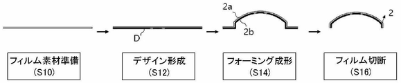
図2は本発明のフィルム2の製作工程を示すフローチャート、図3は図2の製作工程による本発明のフィルム2の段階別形状を示す図である。
図4は本発明の第2プラスチック樹脂6の製作工程を示すフローチャート、図5は図4の製作工程による本発明の第2プラスチック樹脂6の段階別形状を示す図である。
以上の工程によってそれぞれ完成された本発明のフィルム2と、電子回路8及び電子素子10が一体化した第2プラスチック樹脂6とはインサート射出成形工程によって最終的なIME構造1に完成される。
2 フィルム
4 第1プラスチック樹脂
6 第2プラスチック樹脂
8 電子回路
10 電子素子
22 貫通部
100 端子部
Claims (10)
- IME(In-mold electronics)構造であって、デザインが形成されたフィルムと、前記フィルムの下部に位置する第1プラスチック樹脂と、前記第1プラスチック樹脂の下部に位置する第2プラスチック樹脂とを含み、前記第2プラスチック樹脂の上面又は両面にはメッキ工法で電子回路が形成され、電子素子が実装されることにより、前記フィルムと、前記第1プラスチック樹脂と、前記電子回路及び前記電子素子が形成された前記第2プラスチック樹脂とが一体化した、IME構造。
- 前記第1プラスチック樹脂は全体として前記フィルムの形状と類似しており、その上面は前記フィルムの下面と結合され、前記第2プラスチック樹脂の上面全体と側面を完全に取り囲んで密封する高さを有する、請求項1に記載のIME構造。
- 前記第2プラスチック樹脂の高さは前記第1プラスチック樹脂の高さより小さくなるように薄く成形され、左右の幅が前記第1プラスチック樹脂の幅より短く、前記第2プラスチック樹脂の下面全体は外部に露出される、請求項2に記載のIME構造。
- 前記第1プラスチック樹脂の下面は、前記IME構造の最外周縁から前記第2プラスチック樹脂の側面に至る内側まで延びて下方に露出される露出部、及び前記第2プラスチック樹脂の側面及び上面と直接対面して構造的に一体に結合される非露出部の2部分からなる、請求項3に記載のIME構造。
- 前記電子回路の部分と電気的に連結され、前記第2プラスチック樹脂の貫通ホールを通して下方に延びた端子部又は前記電子回路のメッキの際、前記第2プラスチック樹脂の前記貫通ホールを通して前記電子回路の一部が下面に露出されて端子と連結される構造を含む、請求項3に記載のIME構造。
- デザインが形成されたフィルムと、前記フィルムの下部に位置する第1プラスチック樹脂と、前記第1プラスチック樹脂の下部に位置する第2プラスチック樹脂とを含むIME(In-mold electronics)構造の製作方法であって、
弾力性を有するプラスチック樹脂から素材層を製作する段階と、
前記素材層上にシルクスクリーン、パッド、インクジェット、オフセット、又はデジタルプリンティング工程による印刷、蒸着又はUVモールディングによってデザインを形成する段階と、
デザインが形成された前記素材層を熱成形、真空成形又は高圧成形でフォーミングして3次元形状に製作する段階と、
製品の形状に合わせてフォーミングされたフィルムを製品のサイズに合わせて切断する段階とを含む、IME構造の製作方法。 - デザインが形成されたフィルムと、前記フィルムの下部に位置する第1プラスチック樹脂と、前記第1プラスチック樹脂の下部に位置する第2プラスチック樹脂とを含むIME(In-mold electronics)構造の製作方法であって、
前記第2プラスチック樹脂の素材を製品形状に合わせて射出成形する段階であって、貫通ホールを形成することを含む段階と、
射出成形された前記第2プラスチック樹脂の上面又は上面及び下面にメッキ工法で電子回路を形成する段階と、
射出成形された前記第2プラスチック樹脂の両面にメッキ工法で、前記電子回路の形成の際に下面の前記電子回路を保護するための保護層を形成する段階と、
前記電子回路が形成された前記第2プラスチック樹脂の上面又は上面及び下面に、熱損傷を最小化するために、低温硬化性ソルダーペーストを用いた低温ソルダリング方式、又はソルダーペーストが塗布された部位のみ局部加熱する方式を含むソルダリング工法で電子素子を実装する段階とを含む、IME構造の製作方法。 - 前記メッキ工法で電子回路を形成する段階は、
メッキ工程のために、アルカリ性溶液又は酸性溶液で前記第2プラスチック樹脂の上面を前処理する工程と、
前記電子回路がメッキされる領域にレーザーで微細な凹凸を形成する工程と、
前記電子回路の具現のために、伝導性金属をエッチングされた前記凹凸に充填するメッキ工程とを含む、請求項7に記載のIME構造の製作方法。 - デザインが形成されたフィルムと、前記フィルムの下部に位置する第1プラスチック樹脂と、前記第1プラスチック樹脂の下部に位置する第2プラスチック樹脂とを含むIME(In-mold electronics)構造の製作方法であって、
製品の形状に合わせて成形されたフィルムと第2プラスチック樹脂を提供する段階と、
製品形状と同じ形状のキャビティ(cavity)を有するモールドの上部に前記フィルムを装着し、モールドの下部に前記第2プラスチック樹脂を装着する段階と、
キャビティの内部にプラスチック樹脂を注入して充填し、所定の温度及び圧力の下でインサート射出工程を遂行して前記第1プラスチック樹脂を成形することにより、前記フィルムと、前記第1プラスチック樹脂と、前記第2プラスチック樹脂とからなるIME構造を完成する段階とを含む、IME構造の製作方法。 - 前記第2プラスチック樹脂を提供する段階は、
前記第2プラスチック樹脂の素材を製品形状に合わせて射出成形する段階であって、貫通ホールを形成することを含む段階と、
射出成形された前記第2プラスチック樹脂の上面又は両面にメッキ工法で電子回路を形成する段階と、
射出成形された前記第2プラスチック樹脂の両面に、メッキ工法で前記電子回路を形成するときに下面の前記電子回路を保護するための保護層を形成する段階と、
前記電子回路が形成された前記第2プラスチック樹脂の上面又は下面を含む両面に低温ソルダリング工法又は局部加熱方式のソルダリング工法を適用して電子素子を実装する段階とを含む、請求項9に記載のIME構造の製作方法。
Applications Claiming Priority (2)
| Application Number | Priority Date | Filing Date | Title |
|---|---|---|---|
| KR10-2020-0174369 | 2020-12-14 | ||
| KR1020200174369A KR102357563B1 (ko) | 2020-12-14 | 2020-12-14 | 전자회로 도금 공법을 이용한 ime 구조 및 그 제조방법 |
Publications (2)
| Publication Number | Publication Date |
|---|---|
| JP2022094271A true JP2022094271A (ja) | 2022-06-24 |
| JP7264923B2 JP7264923B2 (ja) | 2023-04-25 |
Family
ID=74673099
Family Applications (1)
| Application Number | Title | Priority Date | Filing Date |
|---|---|---|---|
| JP2021018836A Active JP7264923B2 (ja) | 2020-12-14 | 2021-02-09 | 電子回路メッキ工法を用いたime構造及びその製造方法 |
Country Status (5)
| Country | Link |
|---|---|
| US (1) | US20220184865A1 (ja) |
| EP (1) | EP4011593A1 (ja) |
| JP (1) | JP7264923B2 (ja) |
| KR (1) | KR102357563B1 (ja) |
| CN (1) | CN114630493B (ja) |
Families Citing this family (3)
| Publication number | Priority date | Publication date | Assignee | Title |
|---|---|---|---|---|
| KR102791869B1 (ko) * | 2022-02-11 | 2025-04-08 | 인탑스 주식회사 | Ime 조명 인디케이터 구조 |
| KR102697962B1 (ko) * | 2022-04-21 | 2024-08-22 | 인탑스 주식회사 | 전자회로 도금 공법을 이용한 플라스틱 수지 회로 기판 제조 방법 |
| CN116626103B (zh) * | 2023-07-24 | 2023-09-22 | 常州铂力塑胶有限公司 | 一种隔音隔热材料性能检测装置及方法 |
Citations (7)
| Publication number | Priority date | Publication date | Assignee | Title |
|---|---|---|---|---|
| JPH09321427A (ja) * | 1996-05-29 | 1997-12-12 | Nitto Boseki Co Ltd | 射出成形プリント配線板の製造方法 |
| JP2004152934A (ja) * | 2002-10-30 | 2004-05-27 | Mitsui Chemicals Inc | 回路基板およびその製造方法 |
| JP2009130283A (ja) * | 2007-11-27 | 2009-06-11 | Alps Electric Co Ltd | 電子機器用外観ケースおよびその製造方法 |
| JP2012241149A (ja) * | 2011-05-23 | 2012-12-10 | Panasonic Corp | 樹脂組成物及び回路基板の製造方法 |
| JP2017501056A (ja) * | 2013-12-18 | 2017-01-12 | レオンハード クルツ シュティフトゥング ウント コー. カーゲー | プラスチック成形品およびその製造方法 |
| JP2017056624A (ja) * | 2015-09-16 | 2017-03-23 | 凸版印刷株式会社 | 成形品の製造方法 |
| JP2020516487A (ja) * | 2017-04-10 | 2020-06-11 | タクトテク オーユー | 電子アセンブリの製造方法および電子アセンブリ |
Family Cites Families (21)
| Publication number | Priority date | Publication date | Assignee | Title |
|---|---|---|---|---|
| US3077658A (en) * | 1960-04-11 | 1963-02-19 | Gen Dynamics Corp | Method of manufacturing molded module assemblies |
| US3438127A (en) * | 1965-10-21 | 1969-04-15 | Friden Inc | Manufacture of circuit modules using etched molds |
| US3889363A (en) * | 1971-02-16 | 1975-06-17 | Richard P Davis | Method of making printed circuit boards |
| DE3012889C2 (de) * | 1979-04-30 | 1984-01-12 | Kollmorgen Technologies Corp., 75201 Dallas, Tex. | Basismaterial für die Herstellung gedruckter Schaltungen |
| FR2630843B1 (fr) * | 1988-04-28 | 1990-08-03 | Schlumberger Ind Sa | Procede de realisation de cartes comportant des elements graphiques et cartes obtenues par ledit procede |
| US4944908A (en) * | 1988-10-28 | 1990-07-31 | Eaton Corporation | Method for forming a molded plastic article |
| JPH0677648A (ja) * | 1992-08-20 | 1994-03-18 | Polyplastics Co | 立体的多層導電回路を有する複合成形品及びその製造方法 |
| US7225537B2 (en) * | 2005-01-27 | 2007-06-05 | Cardxx, Inc. | Method for making memory cards and similar devices using isotropic thermoset materials with high quality exterior surfaces |
| CN101384425A (zh) * | 2006-02-20 | 2009-03-11 | 大赛璐化学工业株式会社 | 多孔性薄膜及使用了多孔性薄膜的层叠体 |
| US8655481B2 (en) * | 2010-04-09 | 2014-02-18 | Victor Shi-Yueh Sheu | IMR (in-mold roller or in-mold release)/IMF (in-mold forming) making method using a digital printer printing and pre-forming technique |
| US8804344B2 (en) * | 2011-06-10 | 2014-08-12 | Scott Moncrieff | Injection molded control panel with in-molded decorated plastic film |
| KR20130125606A (ko) * | 2012-05-09 | 2013-11-19 | 삼성전자주식회사 | 전자제품 외형케이스와 일체화된 회로필름 |
| KR101282183B1 (ko) * | 2013-02-08 | 2013-07-04 | (주) 우진 더블유.티.피. | 두 단계 전처리 과정을 갖는 엘디에스(lds) 무전해 도금 방법 및 이에 의한 인테나 |
| KR101399912B1 (ko) * | 2013-07-09 | 2014-05-29 | 엘이디라이텍(주) | 저온 공법으로 제작되는 플렉시블 필름기반 엘이디 장식물의 제작방법 |
| CN116872434A (zh) | 2013-09-27 | 2023-10-13 | 塔科图特科有限责任公司 | 用于制造机电结构的方法以及用于执行该方法的装置 |
| DE102014106585A1 (de) * | 2014-05-09 | 2015-11-12 | Leonhard Kurz Stiftung & Co. Kg | Mehrschichtkörper und Verfahren zu dessen Herstellung |
| KR102601370B1 (ko) | 2015-03-27 | 2023-11-13 | 필립모리스 프로덕츠 에스.에이. | 재밀봉 가능한 에어로졸 발생 물품 |
| US10716219B2 (en) | 2017-01-26 | 2020-07-14 | Lite-On Electronics (Guangzhou) Limited | Electronic product and manufacturing method thereof |
| US10057989B1 (en) * | 2017-04-10 | 2018-08-21 | Tactotek Oy | Multilayer structure and related method of manufacture for electronics |
| US11088066B2 (en) * | 2018-03-19 | 2021-08-10 | Tactotek Oy | Multilayer structure and related method of manufacture for electronics |
| US10946612B2 (en) * | 2018-08-27 | 2021-03-16 | Tactotek Oy | Integrated multilayer structure for use in sensing applications and method for manufacturing thereof |
-
2020
- 2020-12-14 KR KR1020200174369A patent/KR102357563B1/ko active Active
-
2021
- 2021-02-09 JP JP2021018836A patent/JP7264923B2/ja active Active
- 2021-02-11 US US17/173,390 patent/US20220184865A1/en not_active Abandoned
- 2021-02-19 CN CN202110191368.0A patent/CN114630493B/zh active Active
- 2021-02-22 EP EP21158443.8A patent/EP4011593A1/en not_active Withdrawn
Patent Citations (7)
| Publication number | Priority date | Publication date | Assignee | Title |
|---|---|---|---|---|
| JPH09321427A (ja) * | 1996-05-29 | 1997-12-12 | Nitto Boseki Co Ltd | 射出成形プリント配線板の製造方法 |
| JP2004152934A (ja) * | 2002-10-30 | 2004-05-27 | Mitsui Chemicals Inc | 回路基板およびその製造方法 |
| JP2009130283A (ja) * | 2007-11-27 | 2009-06-11 | Alps Electric Co Ltd | 電子機器用外観ケースおよびその製造方法 |
| JP2012241149A (ja) * | 2011-05-23 | 2012-12-10 | Panasonic Corp | 樹脂組成物及び回路基板の製造方法 |
| JP2017501056A (ja) * | 2013-12-18 | 2017-01-12 | レオンハード クルツ シュティフトゥング ウント コー. カーゲー | プラスチック成形品およびその製造方法 |
| JP2017056624A (ja) * | 2015-09-16 | 2017-03-23 | 凸版印刷株式会社 | 成形品の製造方法 |
| JP2020516487A (ja) * | 2017-04-10 | 2020-06-11 | タクトテク オーユー | 電子アセンブリの製造方法および電子アセンブリ |
Also Published As
| Publication number | Publication date |
|---|---|
| CN114630493A (zh) | 2022-06-14 |
| JP7264923B2 (ja) | 2023-04-25 |
| US20220184865A1 (en) | 2022-06-16 |
| CN114630493B (zh) | 2024-01-16 |
| EP4011593A1 (en) | 2022-06-15 |
| KR102357563B1 (ko) | 2022-02-07 |
Similar Documents
| Publication | Publication Date | Title |
|---|---|---|
| KR101675793B1 (ko) | 인몰드된 저항 및 차폐 소자 | |
| JP2022094271A (ja) | 電子回路メッキ工法を用いたime構造及びその製造方法 | |
| CN100556240C (zh) | 集成机电设备和生产方法 | |
| CN101444035A (zh) | 密钥卡装置和方法 | |
| KR20100017177A (ko) | 인몰드된 정전용량 방식 스위치 | |
| JP7269297B2 (ja) | 多重ime構造及びその製造方法 | |
| JP2012015578A (ja) | アンテナ装置及びその製造方法 | |
| CN213026099U (zh) | 电致发光壳体 | |
| JP7170010B2 (ja) | 導電回路シート一体化成形品及びその製造方法 | |
| JPH1027983A (ja) | 電磁波シールド機能を有する樹脂製筐体及びその製造方法 | |
| KR102697962B1 (ko) | 전자회로 도금 공법을 이용한 플라스틱 수지 회로 기판 제조 방법 | |
| CN113342188A (zh) | 一种双层薄膜结构的模内电子面板及其制作方法 | |
| CN113965633B (zh) | 一种触碰震动产品及生产方法 | |
| JP2553773Y2 (ja) | 押しボタンスイッチ構造 | |
| TW202112190A (zh) | 觸控模組及其製造方法 | |
| JPH0660934U (ja) | スイッチ付き成形基板 | |
| JP2001266691A (ja) | シート状キートップおよびその製造方法 | |
| JP2002008477A (ja) | 押釦スイッチ用キートップ部材及びその製造方法 | |
| JP2002184255A (ja) | 押ボタンユニットの成形方法 |
Legal Events
| Date | Code | Title | Description |
|---|---|---|---|
| A621 | Written request for application examination |
Free format text: JAPANESE INTERMEDIATE CODE: A621 Effective date: 20210226 |
|
| A131 | Notification of reasons for refusal |
Free format text: JAPANESE INTERMEDIATE CODE: A131 Effective date: 20220301 |
|
| A521 | Request for written amendment filed |
Free format text: JAPANESE INTERMEDIATE CODE: A523 Effective date: 20220601 |
|
| A131 | Notification of reasons for refusal |
Free format text: JAPANESE INTERMEDIATE CODE: A131 Effective date: 20220712 |
|
| A601 | Written request for extension of time |
Free format text: JAPANESE INTERMEDIATE CODE: A601 Effective date: 20221011 |
|
| TRDD | Decision of grant or rejection written | ||
| A01 | Written decision to grant a patent or to grant a registration (utility model) |
Free format text: JAPANESE INTERMEDIATE CODE: A01 Effective date: 20230328 |
|
| A61 | First payment of annual fees (during grant procedure) |
Free format text: JAPANESE INTERMEDIATE CODE: A61 Effective date: 20230413 |
|
| R150 | Certificate of patent or registration of utility model |
Ref document number: 7264923 Country of ref document: JP Free format text: JAPANESE INTERMEDIATE CODE: R150 |
|
| R250 | Receipt of annual fees |
Free format text: JAPANESE INTERMEDIATE CODE: R250 |