JP2022094271A - IME structure using electronic circuit plating method and its manufacturing method - Google Patents
IME structure using electronic circuit plating method and its manufacturing method Download PDFInfo
- Publication number
- JP2022094271A JP2022094271A JP2021018836A JP2021018836A JP2022094271A JP 2022094271 A JP2022094271 A JP 2022094271A JP 2021018836 A JP2021018836 A JP 2021018836A JP 2021018836 A JP2021018836 A JP 2021018836A JP 2022094271 A JP2022094271 A JP 2022094271A
- Authority
- JP
- Japan
- Prior art keywords
- plastic resin
- film
- ime
- electronic circuit
- forming
- Prior art date
- Legal status (The legal status is an assumption and is not a legal conclusion. Google has not performed a legal analysis and makes no representation as to the accuracy of the status listed.)
- Granted
Links
Images


Classifications
-
- B—PERFORMING OPERATIONS; TRANSPORTING
- B29—WORKING OF PLASTICS; WORKING OF SUBSTANCES IN A PLASTIC STATE IN GENERAL
- B29C—SHAPING OR JOINING OF PLASTICS; SHAPING OF MATERIAL IN A PLASTIC STATE, NOT OTHERWISE PROVIDED FOR; AFTER-TREATMENT OF THE SHAPED PRODUCTS, e.g. REPAIRING
- B29C45/00—Injection moulding, i.e. forcing the required volume of moulding material through a nozzle into a closed mould; Apparatus therefor
- B29C45/14—Injection moulding, i.e. forcing the required volume of moulding material through a nozzle into a closed mould; Apparatus therefor incorporating preformed parts or layers, e.g. injection moulding around inserts or for coating articles
- B29C45/14639—Injection moulding, i.e. forcing the required volume of moulding material through a nozzle into a closed mould; Apparatus therefor incorporating preformed parts or layers, e.g. injection moulding around inserts or for coating articles for obtaining an insulating effect, e.g. for electrical components
- B29C45/14655—Injection moulding, i.e. forcing the required volume of moulding material through a nozzle into a closed mould; Apparatus therefor incorporating preformed parts or layers, e.g. injection moulding around inserts or for coating articles for obtaining an insulating effect, e.g. for electrical components connected to or mounted on a carrier, e.g. lead frame
-
- H—ELECTRICITY
- H05—ELECTRIC TECHNIQUES NOT OTHERWISE PROVIDED FOR
- H05K—PRINTED CIRCUITS; CASINGS OR CONSTRUCTIONAL DETAILS OF ELECTRIC APPARATUS; MANUFACTURE OF ASSEMBLAGES OF ELECTRICAL COMPONENTS
- H05K1/00—Printed circuits
- H05K1/18—Printed circuits structurally associated with non-printed electric components
- H05K1/182—Printed circuits structurally associated with non-printed electric components associated with components mounted in the printed circuit board, e.g. insert mounted components [IMC]
- H05K1/185—Components encapsulated in the insulating substrate of the printed circuit or incorporated in internal layers of a multilayer circuit
-
- B—PERFORMING OPERATIONS; TRANSPORTING
- B29—WORKING OF PLASTICS; WORKING OF SUBSTANCES IN A PLASTIC STATE IN GENERAL
- B29C—SHAPING OR JOINING OF PLASTICS; SHAPING OF MATERIAL IN A PLASTIC STATE, NOT OTHERWISE PROVIDED FOR; AFTER-TREATMENT OF THE SHAPED PRODUCTS, e.g. REPAIRING
- B29C45/00—Injection moulding, i.e. forcing the required volume of moulding material through a nozzle into a closed mould; Apparatus therefor
- B29C45/14—Injection moulding, i.e. forcing the required volume of moulding material through a nozzle into a closed mould; Apparatus therefor incorporating preformed parts or layers, e.g. injection moulding around inserts or for coating articles
- B29C45/14778—Injection moulding, i.e. forcing the required volume of moulding material through a nozzle into a closed mould; Apparatus therefor incorporating preformed parts or layers, e.g. injection moulding around inserts or for coating articles the article consisting of a material with particular properties, e.g. porous, brittle
- B29C45/14811—Multilayered articles
-
- B—PERFORMING OPERATIONS; TRANSPORTING
- B29—WORKING OF PLASTICS; WORKING OF SUBSTANCES IN A PLASTIC STATE IN GENERAL
- B29C—SHAPING OR JOINING OF PLASTICS; SHAPING OF MATERIAL IN A PLASTIC STATE, NOT OTHERWISE PROVIDED FOR; AFTER-TREATMENT OF THE SHAPED PRODUCTS, e.g. REPAIRING
- B29C45/00—Injection moulding, i.e. forcing the required volume of moulding material through a nozzle into a closed mould; Apparatus therefor
- B29C45/14—Injection moulding, i.e. forcing the required volume of moulding material through a nozzle into a closed mould; Apparatus therefor incorporating preformed parts or layers, e.g. injection moulding around inserts or for coating articles
- B29C45/14311—Injection moulding, i.e. forcing the required volume of moulding material through a nozzle into a closed mould; Apparatus therefor incorporating preformed parts or layers, e.g. injection moulding around inserts or for coating articles using means for bonding the coating to the articles
-
- B—PERFORMING OPERATIONS; TRANSPORTING
- B29—WORKING OF PLASTICS; WORKING OF SUBSTANCES IN A PLASTIC STATE IN GENERAL
- B29C—SHAPING OR JOINING OF PLASTICS; SHAPING OF MATERIAL IN A PLASTIC STATE, NOT OTHERWISE PROVIDED FOR; AFTER-TREATMENT OF THE SHAPED PRODUCTS, e.g. REPAIRING
- B29C45/00—Injection moulding, i.e. forcing the required volume of moulding material through a nozzle into a closed mould; Apparatus therefor
- B29C45/14—Injection moulding, i.e. forcing the required volume of moulding material through a nozzle into a closed mould; Apparatus therefor incorporating preformed parts or layers, e.g. injection moulding around inserts or for coating articles
- B29C45/14688—Coating articles provided with a decoration
-
- B—PERFORMING OPERATIONS; TRANSPORTING
- B29—WORKING OF PLASTICS; WORKING OF SUBSTANCES IN A PLASTIC STATE IN GENERAL
- B29C—SHAPING OR JOINING OF PLASTICS; SHAPING OF MATERIAL IN A PLASTIC STATE, NOT OTHERWISE PROVIDED FOR; AFTER-TREATMENT OF THE SHAPED PRODUCTS, e.g. REPAIRING
- B29C45/00—Injection moulding, i.e. forcing the required volume of moulding material through a nozzle into a closed mould; Apparatus therefor
- B29C45/16—Making multilayered or multicoloured articles
- B29C45/1642—Making multilayered or multicoloured articles having a "sandwich" structure
- B29C45/1643—Making multilayered or multicoloured articles having a "sandwich" structure from at least three different materials or with at least four layers
-
- B—PERFORMING OPERATIONS; TRANSPORTING
- B29—WORKING OF PLASTICS; WORKING OF SUBSTANCES IN A PLASTIC STATE IN GENERAL
- B29C—SHAPING OR JOINING OF PLASTICS; SHAPING OF MATERIAL IN A PLASTIC STATE, NOT OTHERWISE PROVIDED FOR; AFTER-TREATMENT OF THE SHAPED PRODUCTS, e.g. REPAIRING
- B29C45/00—Injection moulding, i.e. forcing the required volume of moulding material through a nozzle into a closed mould; Apparatus therefor
- B29C45/16—Making multilayered or multicoloured articles
- B29C45/1671—Making multilayered or multicoloured articles with an insert
-
- B—PERFORMING OPERATIONS; TRANSPORTING
- B29—WORKING OF PLASTICS; WORKING OF SUBSTANCES IN A PLASTIC STATE IN GENERAL
- B29D—PRODUCING PARTICULAR ARTICLES FROM PLASTICS OR FROM SUBSTANCES IN A PLASTIC STATE
- B29D7/00—Producing flat articles, e.g. films or sheets
- B29D7/01—Films or sheets
-
- H—ELECTRICITY
- H05—ELECTRIC TECHNIQUES NOT OTHERWISE PROVIDED FOR
- H05K—PRINTED CIRCUITS; CASINGS OR CONSTRUCTIONAL DETAILS OF ELECTRIC APPARATUS; MANUFACTURE OF ASSEMBLAGES OF ELECTRICAL COMPONENTS
- H05K3/00—Apparatus or processes for manufacturing printed circuits
- H05K3/0011—Working of insulating substrates or insulating layers
- H05K3/0014—Shaping of the substrate, e.g. by moulding
-
- H—ELECTRICITY
- H05—ELECTRIC TECHNIQUES NOT OTHERWISE PROVIDED FOR
- H05K—PRINTED CIRCUITS; CASINGS OR CONSTRUCTIONAL DETAILS OF ELECTRIC APPARATUS; MANUFACTURE OF ASSEMBLAGES OF ELECTRICAL COMPONENTS
- H05K3/00—Apparatus or processes for manufacturing printed circuits
- H05K3/30—Assembling printed circuits with electric components, e.g. with resistor
- H05K3/32—Assembling printed circuits with electric components, e.g. with resistor electrically connecting electric components or wires to printed circuits
- H05K3/34—Assembling printed circuits with electric components, e.g. with resistor electrically connecting electric components or wires to printed circuits by soldering
-
- B—PERFORMING OPERATIONS; TRANSPORTING
- B29—WORKING OF PLASTICS; WORKING OF SUBSTANCES IN A PLASTIC STATE IN GENERAL
- B29C—SHAPING OR JOINING OF PLASTICS; SHAPING OF MATERIAL IN A PLASTIC STATE, NOT OTHERWISE PROVIDED FOR; AFTER-TREATMENT OF THE SHAPED PRODUCTS, e.g. REPAIRING
- B29C45/00—Injection moulding, i.e. forcing the required volume of moulding material through a nozzle into a closed mould; Apparatus therefor
- B29C45/14—Injection moulding, i.e. forcing the required volume of moulding material through a nozzle into a closed mould; Apparatus therefor incorporating preformed parts or layers, e.g. injection moulding around inserts or for coating articles
- B29C45/14311—Injection moulding, i.e. forcing the required volume of moulding material through a nozzle into a closed mould; Apparatus therefor incorporating preformed parts or layers, e.g. injection moulding around inserts or for coating articles using means for bonding the coating to the articles
- B29C2045/14327—Injection moulding, i.e. forcing the required volume of moulding material through a nozzle into a closed mould; Apparatus therefor incorporating preformed parts or layers, e.g. injection moulding around inserts or for coating articles using means for bonding the coating to the articles anchoring by forcing the material to pass through a hole in the article
-
- B—PERFORMING OPERATIONS; TRANSPORTING
- B29—WORKING OF PLASTICS; WORKING OF SUBSTANCES IN A PLASTIC STATE IN GENERAL
- B29C—SHAPING OR JOINING OF PLASTICS; SHAPING OF MATERIAL IN A PLASTIC STATE, NOT OTHERWISE PROVIDED FOR; AFTER-TREATMENT OF THE SHAPED PRODUCTS, e.g. REPAIRING
- B29C45/00—Injection moulding, i.e. forcing the required volume of moulding material through a nozzle into a closed mould; Apparatus therefor
- B29C45/14—Injection moulding, i.e. forcing the required volume of moulding material through a nozzle into a closed mould; Apparatus therefor incorporating preformed parts or layers, e.g. injection moulding around inserts or for coating articles
- B29C45/14688—Coating articles provided with a decoration
- B29C2045/14704—Coating articles provided with a decoration ink decorations
-
- B—PERFORMING OPERATIONS; TRANSPORTING
- B29—WORKING OF PLASTICS; WORKING OF SUBSTANCES IN A PLASTIC STATE IN GENERAL
- B29C—SHAPING OR JOINING OF PLASTICS; SHAPING OF MATERIAL IN A PLASTIC STATE, NOT OTHERWISE PROVIDED FOR; AFTER-TREATMENT OF THE SHAPED PRODUCTS, e.g. REPAIRING
- B29C45/00—Injection moulding, i.e. forcing the required volume of moulding material through a nozzle into a closed mould; Apparatus therefor
- B29C45/14—Injection moulding, i.e. forcing the required volume of moulding material through a nozzle into a closed mould; Apparatus therefor incorporating preformed parts or layers, e.g. injection moulding around inserts or for coating articles
- B29C2045/14852—Injection moulding, i.e. forcing the required volume of moulding material through a nozzle into a closed mould; Apparatus therefor incorporating preformed parts or layers, e.g. injection moulding around inserts or for coating articles incorporating articles with a data carrier, e.g. chips
-
- B—PERFORMING OPERATIONS; TRANSPORTING
- B29—WORKING OF PLASTICS; WORKING OF SUBSTANCES IN A PLASTIC STATE IN GENERAL
- B29C—SHAPING OR JOINING OF PLASTICS; SHAPING OF MATERIAL IN A PLASTIC STATE, NOT OTHERWISE PROVIDED FOR; AFTER-TREATMENT OF THE SHAPED PRODUCTS, e.g. REPAIRING
- B29C45/00—Injection moulding, i.e. forcing the required volume of moulding material through a nozzle into a closed mould; Apparatus therefor
- B29C45/16—Making multilayered or multicoloured articles
- B29C45/1671—Making multilayered or multicoloured articles with an insert
- B29C2045/1673—Making multilayered or multicoloured articles with an insert injecting the first layer, then feeding the insert, then injecting the second layer
-
- B—PERFORMING OPERATIONS; TRANSPORTING
- B29—WORKING OF PLASTICS; WORKING OF SUBSTANCES IN A PLASTIC STATE IN GENERAL
- B29L—INDEXING SCHEME ASSOCIATED WITH SUBCLASS B29C, RELATING TO PARTICULAR ARTICLES
- B29L2031/00—Other particular articles
- B29L2031/34—Electrical apparatus, e.g. sparking plugs or parts thereof
- B29L2031/3406—Components, e.g. resistors
Landscapes
- Engineering & Computer Science (AREA)
- Manufacturing & Machinery (AREA)
- Mechanical Engineering (AREA)
- Microelectronics & Electronic Packaging (AREA)
- Injection Moulding Of Plastics Or The Like (AREA)
- Chemical & Material Sciences (AREA)
- Electroplating Methods And Accessories (AREA)
- Structure Of Printed Boards (AREA)
- Manufacturing Of Printed Wiring (AREA)
- Moulds For Moulding Plastics Or The Like (AREA)
- General Chemical & Material Sciences (AREA)
- Chemical Kinetics & Catalysis (AREA)
- Materials Engineering (AREA)
- Metallurgy (AREA)
- Organic Chemistry (AREA)
Abstract
【課題】自動車や家電製品に広範囲に適用可能な堅固で耐久性に優れたIME構造、及びこの構造を迅速で簡便にかつ効率的に製作することができる製造方法を提供する。【解決手段】IME構造は、デザインが形成されたフィルムと、フィルムの下部に位置する第1プラスチック樹脂と、第1プラスチック樹脂の下部に位置する第2プラスチック樹脂とを含み、前記第2プラスチック樹脂の上面又は両面にはメッキ工法で電子回路が形成され、電子素子が実装されることにより、フィルムと、第1プラスチック樹脂と、電子回路及び電子素子が形成された第2プラスチック樹脂とが一体化する。【選択図】 図1The present invention provides a robust and durable IME structure that is widely applicable to automobiles and home appliances, and a manufacturing method that enables the structure to be manufactured quickly, easily, and efficiently. The IME structure includes a film on which a design is formed, a first plastic resin positioned below the film, and a second plastic resin positioned below the first plastic resin, wherein the second plastic resin An electronic circuit is formed on the upper surface or both sides of the film by a plating method, and an electronic element is mounted to integrate the film, the first plastic resin, and the second plastic resin on which the electronic circuit and the electronic element are formed. do. [Selection diagram] Fig. 1
Description
本発明は電子回路メッキ工法を用いたIME(In-mold electronics)構造及びその製造方法に関するものである。 The present invention relates to an IME (In-mold electronics) structure using an electronic circuit plating method and a method for manufacturing the same.
IME(In-mold electronics)技術は印刷された伝導性インクとインモールド装飾技法を統合して3D形状及び機能を具現する技術であり、比較的最近に胎動した。自動車分野では、2012年にフォード社がオーバーヘッドコンソル(overhead console)に初めて商用化した後、飛躍的に発展し、現在には家電製品、医療装備、小売店、携帯用電子機器、国防及び航空の分野に拡張している。 IME (In-mold electronics) technology is a technology that integrates printed conductive ink and in-mold decoration technique to realize 3D shape and function, and has been relatively recently moved. In the automotive sector, after Ford's first commercialization of the overhead console in 2012, it has grown exponentially and is now home appliances, medical equipment, retailers, portable electronics, national defense and aviation. Expanding to the field.
IME技術は、普通、装飾(decoration)、タッチ制御部又はアンテナをプラスチックフィルム上に印刷する1段階、フィルム上に多様な電子部品を実装(surface mounting)する2段階、フィルムを熱成形(thermoforming)して3D形状に製作する3段階、及び3Dフィルムをプラスチック樹脂とインサート成形で一体化する工程からなる。このように製造された完成品は自動車分野では、例えば運転席のダッシュボード又はドアトリムに美麗な外装フィルムとして視認されるように装着され、スマートフォンの画面タッチやプッシュ動作と類似した操作でフィルムをタッチして自動車ドアを開放するかウィンドウを昇降させることができる。IME製品は、自動車に必要な大部分の電気、電子の機能を提供することができ、機械式のボタン、ノブ、リンク、シャフト又はモーターのような部品が必要ではなく、空間を節約することができ、優れたデザインを有する外装品を提供するなどの多くの利点を有する。 The IME technique is usually one step of printing a decoration, a touch control unit or an antenna on a plastic film, two steps of mounting various electronic components on the film, and thermoforming the film. It consists of three steps of manufacturing into a 3D shape, and a step of integrating the 3D film with the plastic resin by insert molding. In the automobile field, the finished product manufactured in this way is attached to the dashboard or door trim of the driver's seat so that it can be visually recognized as a beautiful exterior film, and the film is touched by an operation similar to the screen touch or push operation of a smartphone. You can then open the car door or raise or lower the window. IME products can provide most of the electrical and electronic functions needed for automobiles, eliminating the need for parts like mechanical buttons, knobs, links, shafts or motors, and saving space. It can have many advantages such as providing exterior parts with excellent design.
IME関連従来技術で二つのフィルムを用いて製作する工程は次のようである。 The process of producing using two films by the conventional technique related to IME is as follows.
まず、上部フィルムにデザインを印刷した後、所定の形状になるように成形し、フィルムAを切断する。デザインは、デコレーション、ロゴ、エムブレム、アイテムの作動や機能を示すボタンデザインなどに適用することができ、これらに制限されない。 First, after printing the design on the upper film, it is molded into a predetermined shape and the film A is cut. Designs can be applied to, but are not limited to, decorations, logos, emblems, button designs that indicate the operation or function of an item, and so on.
これとは別に、下部フィルムには伝導性インクで電子回路を印刷した後、電子素子を実装し、リフロー(reflow)工法で電子素子を接合し、上部フィルムと同じ形状に下部フィルムを成形して切断する。 Separately, after printing an electronic circuit on the lower film with conductive ink, the electronic element is mounted, the electronic element is joined by the reflow method, and the lower film is molded into the same shape as the upper film. Disconnect.
そして、上部フィルム、プラスチック樹脂及び下部フィルムをインサート射出成形して最終製品を完成する。 Then, the upper film, the plastic resin and the lower film are insert-injected to complete the final product.
ところが、このような方法によれば、下部フィルムBの形状によって伝導性回路の構成に制約が多く、工程が非常に複雑な欠点がある。 However, according to such a method, there are many restrictions on the configuration of the conductive circuit due to the shape of the lower film B, and there is a drawback that the process is very complicated.
IMEに関連した特許文献を見れば、韓国公開特許第10-2016-0094936号公報は、フィルムを生成し、フィルム上に伝導体及びグラフィックを形成し、フィルム上に電子素子を付着した後、3次元形状を成すように射出成形する内容を開示している。韓国公開特許第10-2017-0130395号公報は、基板上に導電体をスクリーン印刷し、電子素子を実装した後、3次元形状に射出成形する内容を開示している。米国特許公開第2018/0213651号明細書は、フィルム上に導電性回路を形成し、電子素子を実装し、フィルムを熱成形して立体構造を製造する工程を開示している。これらの特許は、単一のフィルム上に電子回路パターンと電子素子を実装し、フィルムをフォーミング(forming)する一般的な内容を開示するという限界がある。 Looking at the patent documents related to IME, Korean Patent Publication No. 10-2016-0094936 discloses a film, forms a conductor and a graphic on the film, attaches an electronic element on the film, and then 3 The contents of injection molding so as to form a three-dimensional shape are disclosed. Korean Publication No. 10-2017-0130395 discloses a content in which a conductor is screen-printed on a substrate, an electronic element is mounted, and then injection-molded into a three-dimensional shape. US Patent Publication No. 2018/0213651 discloses a process of forming a conductive circuit on a film, mounting an electronic element, and thermoforming the film to produce a three-dimensional structure. These patents have the limitation of mounting electronic circuit patterns and electronic devices on a single film and disclosing the general content of forming a film.
発明者は、以上の特許文献を考慮して、複合層を有する新規のIME構造及びその製造方法を開発することになった。 In consideration of the above patent documents, the inventor has decided to develop a new IME structure having a composite layer and a method for producing the same.
したがって、本発明は自動車や家電製品に広範囲に適用可能な堅固で耐久性に優れたIME構造、及びこの構造を迅速で簡便にかつ効率的に製作することができる製造方法を提供することを目的とする。 Therefore, it is an object of the present invention to provide a robust and durable IME structure that can be widely applied to automobiles and home appliances, and a manufacturing method that can quickly, easily, and efficiently manufacture this structure. And.
上述した目的を達成するために、本発明は、IME(In-mold electronics)構造であって、デザインが形成されたフィルムと、フィルムの下部に位置する第1プラスチック樹脂と、第1プラスチック樹脂の下部に位置する第2プラスチック樹脂とを含み、前記第2プラスチック樹脂の上面又は両面にはメッキ工法で電子回路が形成され、電子素子が実装されることにより、フィルムと、第1プラスチック樹脂と、電子回路及び電子素子が形成された第2プラスチック樹脂とが一体化したIME構造を提供する。 In order to achieve the above-mentioned object, the present invention relates to a film having an IME (In-mold electronics) structure in which a design is formed, a first plastic resin located at the bottom of the film, and a first plastic resin. An electronic circuit is formed on the upper surface or both surfaces of the second plastic resin by a plating method, including a second plastic resin located at a lower portion, and an electronic element is mounted to obtain a film, a first plastic resin, and the like. Provided is an IME structure in which an electronic circuit and a second plastic resin on which an electronic element is formed are integrated.
前記第1プラスチック樹脂は全体としてフィルムの形状と類似しており、その上面はフィルムの下面と結合され、第2プラスチック樹脂の上面全体と側面を完全に取り囲んで密封する高さを有することができる。 The first plastic resin is similar in shape to the film as a whole, the upper surface thereof can be bonded to the lower surface of the film, and can have a height that completely surrounds and seals the entire upper surface and the side surface of the second plastic resin. ..
第2プラスチック樹脂の高さは第1プラスチック樹脂の高さより小さくなるように薄く成形され、左右の幅が第1プラスチック樹脂の幅より短く、第2プラスチック樹脂の下面全体は外部に露出されることができる。 The height of the second plastic resin is formed thin so as to be smaller than the height of the first plastic resin, the left and right widths are shorter than the width of the first plastic resin, and the entire lower surface of the second plastic resin is exposed to the outside. Can be done.
第1プラスチック樹脂の下面は、IME構造の最外周縁から第2プラスチック樹脂の側面に至る内側まで延びて下方に露出される露出部、及び第2プラスチック樹脂の側面及び上面と直接対面して構造的に一体に結合される非露出部の2部分からなることができる。 The lower surface of the first plastic resin has a structure that directly faces the exposed portion extending inward from the outermost peripheral edge of the IME structure to the side surface of the second plastic resin and exposed downward, and the side surface and the upper surface of the second plastic resin. It can consist of two parts of an unexposed portion that are integrally coupled together.
電子回路の部分と電気的に連結され、第2プラスチック樹脂の貫通ホールを通して下方に延びた端子部をさらに含むことができる。 It can further include a terminal portion that is electrically connected to a portion of the electronic circuit and extends downward through a through hole in the second plastic resin.
また、本発明は、デザインが形成されたフィルムと、フィルムの下部に位置する第1プラスチック樹脂と、第1プラスチック樹脂の下部に位置する第2プラスチック樹脂とを含むIME(In-mold electronics)構造の製作方法であって、弾力性を有するプラスチック樹脂から素材層を製作する段階と、前記素材層上にシルクスクリーン、パッド、インクジェット、オフセット、又はデジタルプリンティング工程による印刷、蒸着又はUVモールディングによってデザインを形成する段階と、デザインが形成された素材層を熱成形、真空成形又は高圧成形でフォーミングして3次元形状に製作する段階と、製品の形状に合わせてフォーミングされたフィルムを製品のサイズに合わせて切断する段階とを含むIME構造の製作方法を提供する。 Further, the present invention has an IME (In-mold electronics) structure including a film on which a design is formed, a first plastic resin located at the lower part of the film, and a second plastic resin located at the lower part of the first plastic resin. In the manufacturing method of, the stage of manufacturing a material layer from elastic plastic resin and the design by printing, vapor deposition or UV molding by silk screen, pad, inkjet, offset, or digital printing process on the material layer. The stage of forming, the stage of forming the material layer on which the design is formed by hot forming, vacuum forming or high pressure forming into a three-dimensional shape, and the stage of forming a film according to the shape of the product according to the size of the product. Provided is a method for manufacturing an IME structure including a step of cutting.
また、本発明は、デザインが形成されたフィルムと、フィルムの下部に位置する第1プラスチック樹脂と、第1プラスチック樹脂の下部に位置する第2プラスチック樹脂とを含むIME(In-mold electronics)構造の製作方法であって、第2プラスチック樹脂の素材を製品形状に合わせて射出成形する段階であって、貫通ホールを形成することを含む段階と、射出成形された第2プラスチック樹脂の上面又は上面及び下面にメッキ工法で電子回路を形成する段階と、射出成形された第2プラスチック樹脂の両面にメッキ工法で、電子回路の形成の際に下面の電子回路を保護するための保護層を形成する段階と、電子回路が形成された第2プラスチック樹脂の上面又は上面及び下面に、熱損傷を最小化するために、低温硬化性ソルダーペーストを用いた低温ソルダリング方式、又はソルダーペーストが塗布された部位のみ局部加熱する方式を含むソルダリング工法で電子素子を実装する段階とを含むIME構造の製作方法を提供する。 Further, the present invention has an IME (In-mold electronics) structure including a film on which a design is formed, a first plastic resin located at the lower part of the film, and a second plastic resin located at the lower part of the first plastic resin. The method of manufacturing the method, which is a step of injection molding the material of the second plastic resin according to the product shape, including a step of forming a through hole, and a step of forming a through hole, and an upper surface or an upper surface of the injection molded second plastic resin. And at the stage of forming an electronic circuit on the lower surface by the plating method, and by plating on both sides of the injection-molded second plastic resin, a protective layer for protecting the electronic circuit on the lower surface is formed when the electronic circuit is formed. A low temperature soldering method using a low temperature curable solder paste or a solder paste was applied to the upper surface or the upper surface and the lower surface of the second plastic resin in which the electronic circuit was formed. Provided is a method for manufacturing an IME structure including a step of mounting an electronic element by a soldering method including a method of locally heating only a part.
前記メッキ工法で電子回路を形成する段階は、メッキ工程のために、アルカリ性溶液又は酸性溶液で第2プラスチック樹脂の上面を前処理する工程と、電子回路がメッキされる領域にレーザーで微細な凹凸を形成する工程と、電子回路の具現のために、伝導性金属をエッチングされた前記凹凸に充填するメッキ工程とを含むことができる。 The steps of forming an electronic circuit by the plating method include a step of pretreating the upper surface of the second plastic resin with an alkaline solution or an acidic solution for the plating process, and fine unevenness with a laser in the area where the electronic circuit is plated. A step of forming the above-mentioned unevenness and a plating step of filling the etched unevenness with a conductive metal for the realization of an electronic circuit can be included.
また、本発明は、デザインが形成されたフィルムと、フィルムの下部に位置する第1プラスチック樹脂と、第1プラスチック樹脂の下部に位置する第2プラスチック樹脂とを含むIME(In-mold electronics)構造の製作方法であって、製品の形状に合わせて成形されたフィルムと第2プラスチック樹脂を提供する段階と、製品形状と同じ形状のキャビティ(cavity)を有するモールドの上部にフィルムを装着し、モールドの下部に第2プラスチック樹脂を装着する段階と、キャビティの内部にプラスチック樹脂を注入して充填し、所定の温度及び圧力の下でインサート射出工程を遂行して第1プラスチック樹脂を成形することにより、フィルムと、第1プラスチック樹脂と、第2プラスチック樹脂とからなるIME構造を完成する段階とを含むIME構造の製作方法を提供する。 Further, the present invention has an IME (In-mold electronics) structure including a film on which a design is formed, a first plastic resin located at the lower part of the film, and a second plastic resin located at the lower part of the first plastic resin. In the manufacturing method of, the stage of providing a film molded according to the shape of the product and the second plastic resin, and the film is mounted on the upper part of the mold having a cavity having the same shape as the product shape, and the mold is formed. By mounting the second plastic resin in the lower part of the cavity, injecting and filling the inside of the cavity, and performing the insert injection process under a predetermined temperature and pressure to form the first plastic resin. , A method of manufacturing an IME structure including a step of completing an IME structure composed of a film, a first plastic resin, and a second plastic resin.
本発明は先行技術に比べて簡素化した工程を提供し、メッキ工法を適用したプラスチック樹脂の表面に直接電子回路を具現して製品形状による制約を最小化し、耐久性が強く、プラスチック樹脂層の熱損傷を最小化するためのソルダリング工法で多様な電子素子を直接実装することにより、発光及びタッチセンシングなどの多様な機能を発揮するIME構造及びその製造方法を提供する効果を発揮する。 The present invention provides a simplified process as compared with the prior art, embodies an electronic circuit directly on the surface of a plastic resin to which a plating method is applied, minimizes restrictions due to product shape, has strong durability, and is a plastic resin layer. By directly mounting various electronic elements by a soldering method for minimizing thermal damage, it is effective to provide an IME structure and a manufacturing method thereof that exhibit various functions such as light emission and touch sensing.
本発明による各実施例は本発明の理解を助けるための一例に過ぎず、本発明がこのような実施例に限定されるものではない。本発明は各実施例に含まれる個別構成及び個別機能の少なくとも一つ以上の組合せから構成されることができる。 Each embodiment according to the present invention is merely an example for facilitating the understanding of the present invention, and the present invention is not limited to such examples. The present invention can be composed of at least one combination of individual configurations and individual functions included in each embodiment.
<IME構造1>
図1は本発明のIME構造1の構成要素を示す断面図である。IME構造1は、自動車、家電製品、携帯電話などの分野にも適用可能であるが、以下では主に自動車を前提として説明する。
<
FIG. 1 is a cross-sectional view showing a component of the
IME構造1は、上から順にフィルム2と、フィルム2の下部に位置する第1プラスチック樹脂4と、第1プラスチック樹脂4の下部に位置する第2プラスチック樹脂6とを含む。第2プラスチック樹脂6の上面6a又は上面6a及び下面6bを含む両面には電子回路8及び電子素子10が形成される。IME構造1は、所定のデザインが形成されたフィルム2と、第1プラスチック樹脂4と、電子回路8及び電子素子10などが形成された第2プラスチック樹脂6とが一体化した構造である。
The
フィルム2には、デコレーション、ロゴ、エムブレム、アイテムの作動や機能を示すボタンアイコンなどのデザインDが形成されている。フィルム素材はPC、PMMA、PET、TPUなどの多様な素材が適用可能であり、制限されない。フィルム2は中央が膨らんでいる曲面で、左右両側は平面である全体としてディスク形を例示したが、これに限定されない。フィルム2に照明部が透過することができるように、印刷層又はデザイン構成層に貫通部22が形成される。フィルム2の上面2aは外部に露出されて視認され、貫通部22を通して、例えばLEDのような電子素子10の光が発光することができる。
The
第1プラスチック樹脂4は全体としてフィルム2の形状と類似しており、上面4aがフィルム2の下面2bと結合されるが、側面4cの高さは十分に高いので、第1プラスチック樹脂4は第2プラスチック樹脂6の上面6a全体と側面6cを完全に取り囲んで密封する堅固で厚い構造を有する。樹脂の種類はPC、アクリル、ABS、AESなどのいずれも適宜使うことができるが、これらに制限されない。
The first
第2プラスチック樹脂6はフィルム2と類似したディスク形を有するが、その高さが第1プラスチック樹脂4より小さくなるように薄く成形され、左右の幅が第1プラスチック樹脂4の幅より短いので、前述したように、その上面6aと側面6cが第1プラスチック樹脂4によって完全に覆われる。しかし、第2プラスチック樹脂6の下面6b全体は外部に露出され、上面6aと同じ形状を有する。よって、第1プラスチック樹脂4の下面4bは、IME構造1の最外周縁から側面6cに至る内側まで延びて下に露出される露出部4b1、及び第2プラスチック樹脂の側面6c及び上面6aと直接対面して構造的に一体に結合される非露出部4b2の2部分からなる。樹脂の種類としては、PC、アクリル、ABS、AESなどのいずれも適宜使うことができるが、これらに制限されない。
The second
電子回路8は、電子素子10に電流又は電源を供給するための回路パターン、ケーブル又は導電性インクなどを含み、特に制限されない。電子回路8は、後述するように、メッキ工法によって第2プラスチック樹脂6の上面6a又は上面6a及び下面6bに形成され、所要仕様によって適宜選択可能である。
The
電子素子10は、LED素子、静電容量センサー、チップ、プロセッサ、電気スイッチなどを含み、IME構造1の用途によっていずれでも適宜選択されて第2プラスチック樹脂6の上面6a又は上面6a及び下面6bに実装(surface mounting)される。
The
また、電子回路8とメインボード(図示せず)のコネックティングのために電子回路8の部分と電気的に連結され、第2プラスチック樹脂6の上面6aに形成された電子回路の一部と接地されたフレキシブルプリント基板(FPCB)又は金属ピンが貫通ホール6’を通過して第2プラスチック樹脂6の下面6bに露出される端子部100が形成されるか、又は電子回路が第2プラスチック樹脂6の上面6aから下面6bに延びた電子回路の一部に接地されて端子部100が形成される。これについては図7を参照して後述する。
Further, the
第2プラスチック樹脂6に形成される電子回路8及び電子素子10は、前述したように、上面6aは第1プラスチック樹脂4、下面6bは別途のコーティング層によって取り囲まれて封止されるので、外部の衝撃、変形又は破損に対して十分な耐久性を有する。
As described above, the
また、第2プラスチック樹脂6の下面6bに電子回路8及び電子素子10が形成されない構造では別途のコーティング層は必要でない。
Further, in the structure in which the
以上説明した本発明のIME構造1は以下で説明するそれぞれの構成要件の制作工程によって構造的な意味と物性の特徴がより明らかになるであろう。
In the
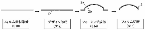
<フィルム2の製作工程>
図2は本発明のフィルム2の製作工程を示すフローチャート、図3は図2の製作工程による本発明のフィルム2の段階別形状を示す図である。
<Production process of
FIG. 2 is a flowchart showing a manufacturing process of the
両図を一緒に参照すると、まず本発明のフィルム2の素材を平面状に準備する(S10)。フィルム2の素材は、PC、PMMA、PET、TPUなどの弾力性を有する多様な素材であれば適用可能であり、制限されない。
Referring to both figures together, first, the material of the
ついで、前記素材層上にデザインDを印刷する(S12)。デザインDの印刷工程は、シルクスクリーン、パッド、インクジェット、オフセット、デジタルプリンティング工程によって遂行することができる。デザインDは、プリンティングだけでなく、蒸着、UVモールディングの方法で形成することができる。 Then, the design D is printed on the material layer (S12). The printing process of Design D can be performed by silk screen, pad, inkjet, offset, digital printing process. The design D can be formed not only by printing but also by vapor deposition and UV molding.
ついで、このように完成された中間材であるフィルムをフォーミング(forming)して、図示のように、3次元形状に成形する(S14)。フォーミング工程は、主に熱成形、真空成形、高圧成形方式で遂行し、フォーミング作業によって製品形状に合う3次元形状に製作される。 Then, the film which is the intermediate material thus completed is formed and formed into a three-dimensional shape as shown in the figure (S14). The forming process is mainly carried out by thermoforming, vacuum forming, and high-pressure forming, and is manufactured into a three-dimensional shape that matches the product shape by forming work.
ついで、製品形状に合わせてフォーミングされたフィルムを製品サイズに合わせて切断する(S16)。切断工程は、プレス打抜き、CNC加工、レーザー加工の工法で遂行することができる。 Then, the film formed according to the product shape is cut according to the product size (S16). The cutting process can be carried out by a method of press punching, CNC processing, or laser processing.
<電子回路8及び電子素子10を備えた第2プラスチック樹脂6の製作工程>
図4は本発明の第2プラスチック樹脂6の製作工程を示すフローチャート、図5は図4の製作工程による本発明の第2プラスチック樹脂6の段階別形状を示す図である。
<Manufacturing process of the second
FIG. 4 is a flowchart showing a manufacturing process of the second
まず、第2プラスチック樹脂6を製品形状に合わせて射出成形する(S20)。この射出成形工程で、端子部100のための貫通ホール6’を同時に形成する。
First, the second
ついで、射出成形された第2プラスチック樹脂6の上面6a又は上面6a及び下面6bを含む両面にメッキ工法で電子回路8を形成する(S22)。エンジニアリングプラスチックメッキ工法は、前処理、エッチング及び電子回路8メッキ工程を含む。メッキ工法は素材の制約なしに多様な形状のパターンを具現することができ、突出した層構造を有しない点で他の工法に比べて有利である。
Then, the
図6は本発明のメッキ工程を適用した電子回路形成の一例を示している。前処理工程では、メッキ工程のためにアルカリ性溶液又は酸性溶液でメッキすべき表面、つまり第2プラスチック樹脂6の上面6a又は上面6a及び下面6bを前処理する。電子回路として使われる金属との密着性及び表面状態を考慮して、水洗、脱脂(cleaning)及び触媒活性化工程を経る。エッチング作業では、電子回路8がメッキされる領域にレーザーで微細な凹凸8bを形成する。メッキ工程では、電子回路8の具現のために、伝導性金属をエッチングされた前記凹凸8bに充填する。メッキは、エッチングと前処理工程を経たので、電解メッキ方式よりは無電解メッキ方式を用いることが好ましい。
FIG. 6 shows an example of electronic circuit formation to which the plating process of the present invention is applied. In the pretreatment step, the surface to be plated with an alkaline solution or an acidic solution for the plating step, that is, the
ついで、電子回路8が形成された第2プラスチック樹脂6の上面6a又は上面6a及び下面6bの両面に電子素子10を実装する(S24)。電子素子10は、LED、ICチップなどの電気的機能を有する素材を使う。ここで、第2プラスチック樹脂6の熱損傷を最小化するために、低温ソルダリング工法を適用する。具体的に、低温硬化性ソルダーペーストを塗布して接合する方式と、一般的なソルダーペーストが塗布された部位のみ局部加熱する接合方式とによって第2プラスチック樹脂6の熱損傷を最小化することができ、所要仕様によって選択的に用いる。電子素子10を実装しながらリフロー(reflow)作業を行うことにより、電気素子10のピンを溶融して表面に固定する。リフロー作業は第2プラスチック樹脂6の熱損傷を最小化する温度以下で実施することが好ましい。
Then, the
ついで、第2プラスチック樹脂6の下面に電子回路8及び電子素子10を形成した場合、コーティング層を形成して、外部の衝撃、変形又は破損に対する十分な耐久性を有するようにする(S26)。
Then, when the
次に、図7を参照して本発明の電気連結構造について説明する。 Next, the electrically connected structure of the present invention will be described with reference to FIG. 7.
まず、図7aは、電子回路8のメッキの際、貫通ホール6’を通して第2プラスチック樹脂6の上面6aから下面6bまで電子回路を延ばして露出させた後、拡大図に示すようなコネクター端子、パッド又はフレキシブルプリント基板(FPCB)を用いてメインボードと連結させる構造を示している。この場合、前記構成要件が図1の端子部100に相当すると言える。
First, in FIG. 7a, when plating the
これとは違い、図7bは、貫通ホール6’を通して端子部100を電子回路8と電気的に連結させるとともにこれを下方に延ばして露出させる構造を示している。端子部100はフレキシブルプリント基板(FPCB)、パッド又は伝導性金属ピンからなる。
Unlike this, FIG. 7b shows a structure in which the
端子部100はメインボード(図示せず)と電気的に接続するように下方に露出される。図7bは端子部100が接地された状態を示す。貫通ホール6’は中央又は側面などの適切な部位に形成される。
The
電子回路8及び電子素子10は第2プラスチック樹脂6の上面6a又は両面に固定され、メインボードから電源が印加されれば、端子部100を介して電源が供給され、電子回路8に属する伝導性パターンを介して電流が供給され、例えばLEDのような電子素子10が発光するなど、自動車機能の具現のための多様な機能を果たすことができる。自動車の電装部品のために使われる場合、タッチセンサー(静電容量及び静電圧方式)又は発光機能を具現することができる。
The
<フィルム2と第2プラスチック樹脂6の結合工程>
以上の工程によってそれぞれ完成された本発明のフィルム2と、電子回路8及び電子素子10が一体化した第2プラスチック樹脂6とはインサート射出成形工程によって最終的なIME構造1に完成される。
<Combination process of
The
フィルム2と第2プラスチック樹脂6は既に製品の形状に合わせて成形されているので、図1で説明した第1プラスチック樹脂4の形成のために、完成製品の形状と同じ形状のキャビティ(cavity)を有するモールド又は金型を準備する。ついで、モールドの上部にフィルム2を装着し、モールドの下部には電子回路8及び電子素子10が一体化した第2プラスチック樹脂6を装着した後、キャビティの内部にプラスチック樹脂を注入して充填し、所定の温度及び圧力の下でインサート射出工程を遂行する。すると、第1プラスチック樹脂4が成形されるにつれて、フィルム2と、フィルム2の下部に位置する第1プラスチック樹脂4と、第1プラスチック樹脂4の下部に位置する第2プラスチック樹脂6とからなるIME構造1が出来上がる。
Since the
第1プラスチック樹脂4の素材は、第2プラスチック樹脂6と同様に制限がないが、例えば電子素子10がタッチ式センサーの場合には、フィルム2を押す指の力が充分に伝達されるように弾力性を有する素材であることが好ましい。
The material of the first
以上で本発明の実施例を説明したが、これは本発明を限定せず、本発明の多様な変形及び修正が可能である。本発明の権利範囲は以下で記述する請求範囲と同一又は均等な範囲まで及ぶというのは自明である。 Although the embodiment of the present invention has been described above, this does not limit the present invention, and various modifications and modifications of the present invention are possible. It is self-evident that the scope of the invention extends to the same or equal scope as the claims described below.
1 IME構造
2 フィルム
4 第1プラスチック樹脂
6 第2プラスチック樹脂
8 電子回路
10 電子素子
22 貫通部
100 端子部
1
Claims (10)
弾力性を有するプラスチック樹脂から素材層を製作する段階と、
前記素材層上にシルクスクリーン、パッド、インクジェット、オフセット、又はデジタルプリンティング工程による印刷、蒸着又はUVモールディングによってデザインを形成する段階と、
デザインが形成された前記素材層を熱成形、真空成形又は高圧成形でフォーミングして3次元形状に製作する段階と、
製品の形状に合わせてフォーミングされたフィルムを製品のサイズに合わせて切断する段階とを含む、IME構造の製作方法。 A method for manufacturing an IME (In-mold electronics) structure including a film on which a design is formed, a first plastic resin located at the bottom of the film, and a second plastic resin located at the bottom of the first plastic resin. There,
At the stage of making a material layer from elastic plastic resin,
The steps of forming a design on the material layer by silkscreening, padding, inkjet, offset, or digital printing, vapor deposition, or UV molding.
At the stage of forming the material layer on which the design is formed by thermoforming, vacuum forming or high pressure forming into a three-dimensional shape,
A method for producing an IME structure, which comprises a step of cutting a film formed according to the shape of a product according to the size of the product.
前記第2プラスチック樹脂の素材を製品形状に合わせて射出成形する段階であって、貫通ホールを形成することを含む段階と、
射出成形された前記第2プラスチック樹脂の上面又は上面及び下面にメッキ工法で電子回路を形成する段階と、
射出成形された前記第2プラスチック樹脂の両面にメッキ工法で、前記電子回路の形成の際に下面の前記電子回路を保護するための保護層を形成する段階と、
前記電子回路が形成された前記第2プラスチック樹脂の上面又は上面及び下面に、熱損傷を最小化するために、低温硬化性ソルダーペーストを用いた低温ソルダリング方式、又はソルダーペーストが塗布された部位のみ局部加熱する方式を含むソルダリング工法で電子素子を実装する段階とを含む、IME構造の製作方法。 A method for manufacturing an IME (In-mold electronics) structure including a film on which a design is formed, a first plastic resin located at the bottom of the film, and a second plastic resin located at the bottom of the first plastic resin. There,
A step of injection molding the second plastic resin material according to the product shape, including a step of forming a through hole, and a step of forming a through hole.
At the stage of forming an electronic circuit on the upper surface or the upper surface and the lower surface of the injection-molded second plastic resin by a plating method, and
At the stage of forming a protective layer for protecting the electronic circuit on the lower surface at the time of forming the electronic circuit by a plating method on both sides of the injection-molded second plastic resin,
A low-temperature soldering method using a low-temperature curable solder paste or a portion to which the solder paste is applied on the upper surface, the upper surface, and the lower surface of the second plastic resin on which the electronic circuit is formed, in order to minimize heat damage. A method for manufacturing an IME structure, including a step of mounting an electronic element by a soldering method including a method of locally heating only.
メッキ工程のために、アルカリ性溶液又は酸性溶液で前記第2プラスチック樹脂の上面を前処理する工程と、
前記電子回路がメッキされる領域にレーザーで微細な凹凸を形成する工程と、
前記電子回路の具現のために、伝導性金属をエッチングされた前記凹凸に充填するメッキ工程とを含む、請求項7に記載のIME構造の製作方法。 The stage of forming an electronic circuit by the plating method is
For the plating step, a step of pretreating the upper surface of the second plastic resin with an alkaline solution or an acidic solution, and a step of pretreating the upper surface of the second plastic resin.
The process of forming fine irregularities with a laser in the area where the electronic circuit is plated, and
The method for manufacturing an IME structure according to claim 7, further comprising a plating step of filling the unevenness with which the conductive metal is etched for the realization of the electronic circuit.
製品の形状に合わせて成形されたフィルムと第2プラスチック樹脂を提供する段階と、
製品形状と同じ形状のキャビティ(cavity)を有するモールドの上部に前記フィルムを装着し、モールドの下部に前記第2プラスチック樹脂を装着する段階と、
キャビティの内部にプラスチック樹脂を注入して充填し、所定の温度及び圧力の下でインサート射出工程を遂行して前記第1プラスチック樹脂を成形することにより、前記フィルムと、前記第1プラスチック樹脂と、前記第2プラスチック樹脂とからなるIME構造を完成する段階とを含む、IME構造の製作方法。 A method for manufacturing an IME (In-mold electronics) structure including a film on which a design is formed, a first plastic resin located at the bottom of the film, and a second plastic resin located at the bottom of the first plastic resin. There,
At the stage of providing a film and a second plastic resin molded according to the shape of the product,
The stage where the film is mounted on the upper part of the mold having a cavity having the same shape as the product shape, and the second plastic resin is mounted on the lower part of the mold.
The film, the first plastic resin, and the like are formed by injecting and filling the inside of the cavity with a plastic resin and performing an insert injection step under a predetermined temperature and pressure to form the first plastic resin. A method for manufacturing an IME structure, which comprises a stage of completing the IME structure made of the second plastic resin.
前記第2プラスチック樹脂の素材を製品形状に合わせて射出成形する段階であって、貫通ホールを形成することを含む段階と、
射出成形された前記第2プラスチック樹脂の上面又は両面にメッキ工法で電子回路を形成する段階と、
射出成形された前記第2プラスチック樹脂の両面に、メッキ工法で前記電子回路を形成するときに下面の前記電子回路を保護するための保護層を形成する段階と、
前記電子回路が形成された前記第2プラスチック樹脂の上面又は下面を含む両面に低温ソルダリング工法又は局部加熱方式のソルダリング工法を適用して電子素子を実装する段階とを含む、請求項9に記載のIME構造の製作方法。 The stage of providing the second plastic resin is
A step of injection molding the second plastic resin material according to the product shape, including a step of forming a through hole, and a step of forming a through hole.
At the stage of forming an electronic circuit on the upper surface or both sides of the injection-molded second plastic resin by a plating method, and
A step of forming a protective layer for protecting the electronic circuit on the lower surface when the electronic circuit is formed by a plating method on both sides of the injection-molded second plastic resin.
The ninth aspect of the present invention includes a step of mounting an electronic element by applying a low-temperature soldering method or a local heating method of soldering to both surfaces including the upper surface or the lower surface of the second plastic resin on which the electronic circuit is formed. The method for manufacturing the described IME structure.
Applications Claiming Priority (2)
| Application Number | Priority Date | Filing Date | Title |
|---|---|---|---|
| KR10-2020-0174369 | 2020-12-14 | ||
| KR1020200174369A KR102357563B1 (en) | 2020-12-14 | 2020-12-14 | In-mold electronics structure using engineering plastic plating process and method therefor |
Publications (2)
| Publication Number | Publication Date |
|---|---|
| JP2022094271A true JP2022094271A (en) | 2022-06-24 |
| JP7264923B2 JP7264923B2 (en) | 2023-04-25 |
Family
ID=74673099
Family Applications (1)
| Application Number | Title | Priority Date | Filing Date |
|---|---|---|---|
| JP2021018836A Active JP7264923B2 (en) | 2020-12-14 | 2021-02-09 | IME structure using electronic circuit plating method and its manufacturing method |
Country Status (5)
| Country | Link |
|---|---|
| US (1) | US20220184865A1 (en) |
| EP (1) | EP4011593A1 (en) |
| JP (1) | JP7264923B2 (en) |
| KR (1) | KR102357563B1 (en) |
| CN (1) | CN114630493B (en) |
Families Citing this family (3)
| Publication number | Priority date | Publication date | Assignee | Title |
|---|---|---|---|---|
| KR102791869B1 (en) * | 2022-02-11 | 2025-04-08 | 인탑스 주식회사 | In-mold electronics illumination structure |
| KR102697962B1 (en) * | 2022-04-21 | 2024-08-22 | 인탑스 주식회사 | Plastic resin circuit board manufacturing method using electronic circuit plating process |
| CN116626103B (en) * | 2023-07-24 | 2023-09-22 | 常州铂力塑胶有限公司 | Sound and heat insulation material performance detection device and method |
Citations (7)
| Publication number | Priority date | Publication date | Assignee | Title |
|---|---|---|---|---|
| JPH09321427A (en) * | 1996-05-29 | 1997-12-12 | Nitto Boseki Co Ltd | Injection-molded printed wiring board manufacturing method |
| JP2004152934A (en) * | 2002-10-30 | 2004-05-27 | Mitsui Chemicals Inc | Circuit board and its manufacturing method |
| JP2009130283A (en) * | 2007-11-27 | 2009-06-11 | Alps Electric Co Ltd | External case for electronic apparatus, and manufacturing method thereof |
| JP2012241149A (en) * | 2011-05-23 | 2012-12-10 | Panasonic Corp | Resin composition and method for manufacturing circuit board |
| JP2017501056A (en) * | 2013-12-18 | 2017-01-12 | レオンハード クルツ シュティフトゥング ウント コー. カーゲー | Plastic molded product and manufacturing method thereof |
| JP2017056624A (en) * | 2015-09-16 | 2017-03-23 | 凸版印刷株式会社 | Production method of molding |
| JP2020516487A (en) * | 2017-04-10 | 2020-06-11 | タクトテク オーユー | Electronic assembly manufacturing method and electronic assembly |
Family Cites Families (21)
| Publication number | Priority date | Publication date | Assignee | Title |
|---|---|---|---|---|
| US3077658A (en) * | 1960-04-11 | 1963-02-19 | Gen Dynamics Corp | Method of manufacturing molded module assemblies |
| US3438127A (en) * | 1965-10-21 | 1969-04-15 | Friden Inc | Manufacture of circuit modules using etched molds |
| US3889363A (en) * | 1971-02-16 | 1975-06-17 | Richard P Davis | Method of making printed circuit boards |
| DE3012889C2 (en) * | 1979-04-30 | 1984-01-12 | Kollmorgen Technologies Corp., 75201 Dallas, Tex. | Base material for the manufacture of printed circuits |
| FR2630843B1 (en) * | 1988-04-28 | 1990-08-03 | Schlumberger Ind Sa | PROCESS FOR PRODUCING CARDS COMPRISING GRAPHIC ELEMENTS AND CARDS OBTAINED BY SAID METHOD |
| US4944908A (en) * | 1988-10-28 | 1990-07-31 | Eaton Corporation | Method for forming a molded plastic article |
| JPH0677648A (en) * | 1992-08-20 | 1994-03-18 | Polyplastics Co | Composite molded item having three-dimensional multilayer conductive circuit and production thereof |
| US7225537B2 (en) * | 2005-01-27 | 2007-06-05 | Cardxx, Inc. | Method for making memory cards and similar devices using isotropic thermoset materials with high quality exterior surfaces |
| CN101384425A (en) * | 2006-02-20 | 2009-03-11 | 大赛璐化学工业株式会社 | Porous film and laminate using porous film |
| US8655481B2 (en) * | 2010-04-09 | 2014-02-18 | Victor Shi-Yueh Sheu | IMR (in-mold roller or in-mold release)/IMF (in-mold forming) making method using a digital printer printing and pre-forming technique |
| US8804344B2 (en) * | 2011-06-10 | 2014-08-12 | Scott Moncrieff | Injection molded control panel with in-molded decorated plastic film |
| KR20130125606A (en) * | 2012-05-09 | 2013-11-19 | 삼성전자주식회사 | Circuit film integrated electronic goods case |
| KR101282183B1 (en) * | 2013-02-08 | 2013-07-04 | (주) 우진 더블유.티.피. | Laser direct structuring electroless plating method with two-step pre-treatment process and intenna thereof |
| KR101399912B1 (en) * | 2013-07-09 | 2014-05-29 | 엘이디라이텍(주) | A led ornament manufacturing method of low temperature based on flexible film |
| CN116872434A (en) | 2013-09-27 | 2023-10-13 | 塔科图特科有限责任公司 | Method for manufacturing electromechanical structures and apparatus for performing the method |
| DE102014106585A1 (en) * | 2014-05-09 | 2015-11-12 | Leonhard Kurz Stiftung & Co. Kg | Multilayer body and method for its production |
| KR102601370B1 (en) | 2015-03-27 | 2023-11-13 | 필립모리스 프로덕츠 에스.에이. | Resealable aerosol-generating items |
| US10716219B2 (en) | 2017-01-26 | 2020-07-14 | Lite-On Electronics (Guangzhou) Limited | Electronic product and manufacturing method thereof |
| US10057989B1 (en) * | 2017-04-10 | 2018-08-21 | Tactotek Oy | Multilayer structure and related method of manufacture for electronics |
| US11088066B2 (en) * | 2018-03-19 | 2021-08-10 | Tactotek Oy | Multilayer structure and related method of manufacture for electronics |
| US10946612B2 (en) * | 2018-08-27 | 2021-03-16 | Tactotek Oy | Integrated multilayer structure for use in sensing applications and method for manufacturing thereof |
-
2020
- 2020-12-14 KR KR1020200174369A patent/KR102357563B1/en active Active
-
2021
- 2021-02-09 JP JP2021018836A patent/JP7264923B2/en active Active
- 2021-02-11 US US17/173,390 patent/US20220184865A1/en not_active Abandoned
- 2021-02-19 CN CN202110191368.0A patent/CN114630493B/en active Active
- 2021-02-22 EP EP21158443.8A patent/EP4011593A1/en not_active Withdrawn
Patent Citations (7)
| Publication number | Priority date | Publication date | Assignee | Title |
|---|---|---|---|---|
| JPH09321427A (en) * | 1996-05-29 | 1997-12-12 | Nitto Boseki Co Ltd | Injection-molded printed wiring board manufacturing method |
| JP2004152934A (en) * | 2002-10-30 | 2004-05-27 | Mitsui Chemicals Inc | Circuit board and its manufacturing method |
| JP2009130283A (en) * | 2007-11-27 | 2009-06-11 | Alps Electric Co Ltd | External case for electronic apparatus, and manufacturing method thereof |
| JP2012241149A (en) * | 2011-05-23 | 2012-12-10 | Panasonic Corp | Resin composition and method for manufacturing circuit board |
| JP2017501056A (en) * | 2013-12-18 | 2017-01-12 | レオンハード クルツ シュティフトゥング ウント コー. カーゲー | Plastic molded product and manufacturing method thereof |
| JP2017056624A (en) * | 2015-09-16 | 2017-03-23 | 凸版印刷株式会社 | Production method of molding |
| JP2020516487A (en) * | 2017-04-10 | 2020-06-11 | タクトテク オーユー | Electronic assembly manufacturing method and electronic assembly |
Also Published As
| Publication number | Publication date |
|---|---|
| CN114630493A (en) | 2022-06-14 |
| JP7264923B2 (en) | 2023-04-25 |
| US20220184865A1 (en) | 2022-06-16 |
| CN114630493B (en) | 2024-01-16 |
| EP4011593A1 (en) | 2022-06-15 |
| KR102357563B1 (en) | 2022-02-07 |
Similar Documents
| Publication | Publication Date | Title |
|---|---|---|
| KR101675793B1 (en) | In-molded resistive and shielding elements | |
| JP2022094271A (en) | IME structure using electronic circuit plating method and its manufacturing method | |
| CN100556240C (en) | Integrated electromechanical devices and production methods | |
| CN101444035A (en) | Key fob device and method | |
| KR20100017177A (en) | In-molded capacitive switch | |
| JP7269297B2 (en) | Multiple IME structure and manufacturing method thereof | |
| JP2012015578A (en) | Antenna device and method for manufacturing the same | |
| CN213026099U (en) | Electroluminescent housing | |
| JP7170010B2 (en) | Conductive circuit sheet integrated molded product and its manufacturing method | |
| JPH1027983A (en) | Resin housing having electromagnetic wave shielding function and method of manufacturing the same | |
| KR102697962B1 (en) | Plastic resin circuit board manufacturing method using electronic circuit plating process | |
| CN113342188A (en) | In-mold electronic panel with double-layer thin film structure and manufacturing method thereof | |
| CN113965633B (en) | Touch vibration product and production method thereof | |
| JP2553773Y2 (en) | Push button switch structure | |
| TW202112190A (en) | Touch module and manufacturing method thereof | |
| JPH0660934U (en) | Molded substrate with switch | |
| JP2001266691A (en) | Sheet-like key top and manufacturing method thereof | |
| JP2002008477A (en) | Key top member for push button switch and manufacturing method of the same | |
| JP2002184255A (en) | Method for molding push button unit |
Legal Events
| Date | Code | Title | Description |
|---|---|---|---|
| A621 | Written request for application examination |
Free format text: JAPANESE INTERMEDIATE CODE: A621 Effective date: 20210226 |
|
| A131 | Notification of reasons for refusal |
Free format text: JAPANESE INTERMEDIATE CODE: A131 Effective date: 20220301 |
|
| A521 | Request for written amendment filed |
Free format text: JAPANESE INTERMEDIATE CODE: A523 Effective date: 20220601 |
|
| A131 | Notification of reasons for refusal |
Free format text: JAPANESE INTERMEDIATE CODE: A131 Effective date: 20220712 |
|
| A601 | Written request for extension of time |
Free format text: JAPANESE INTERMEDIATE CODE: A601 Effective date: 20221011 |
|
| TRDD | Decision of grant or rejection written | ||
| A01 | Written decision to grant a patent or to grant a registration (utility model) |
Free format text: JAPANESE INTERMEDIATE CODE: A01 Effective date: 20230328 |
|
| A61 | First payment of annual fees (during grant procedure) |
Free format text: JAPANESE INTERMEDIATE CODE: A61 Effective date: 20230413 |
|
| R150 | Certificate of patent or registration of utility model |
Ref document number: 7264923 Country of ref document: JP Free format text: JAPANESE INTERMEDIATE CODE: R150 |
|
| R250 | Receipt of annual fees |
Free format text: JAPANESE INTERMEDIATE CODE: R250 |