JP2014086728A - 発光素子 - Google Patents
発光素子 Download PDFInfo
- Publication number
- JP2014086728A JP2014086728A JP2013217084A JP2013217084A JP2014086728A JP 2014086728 A JP2014086728 A JP 2014086728A JP 2013217084 A JP2013217084 A JP 2013217084A JP 2013217084 A JP2013217084 A JP 2013217084A JP 2014086728 A JP2014086728 A JP 2014086728A
- Authority
- JP
- Japan
- Prior art keywords
- light emitting
- emitting device
- electrode
- via electrode
- light
- Prior art date
- Legal status (The legal status is an assumption and is not a legal conclusion. Google has not performed a legal analysis and makes no representation as to the accuracy of the status listed.)
- Pending
Links
Images


Classifications
-
- H—ELECTRICITY
- H01—ELECTRIC ELEMENTS
- H01L—SEMICONDUCTOR DEVICES NOT COVERED BY CLASS H10
- H01L33/00—Semiconductor devices with at least one potential-jump barrier or surface barrier specially adapted for light emission; Processes or apparatus specially adapted for the manufacture or treatment thereof or of parts thereof; Details thereof
- H01L33/48—Semiconductor devices with at least one potential-jump barrier or surface barrier specially adapted for light emission; Processes or apparatus specially adapted for the manufacture or treatment thereof or of parts thereof; Details thereof characterised by the semiconductor body packages
- H01L33/62—Arrangements for conducting electric current to or from the semiconductor body, e.g. lead-frames, wire-bonds or solder balls
-
- H—ELECTRICITY
- H01—ELECTRIC ELEMENTS
- H01L—SEMICONDUCTOR DEVICES NOT COVERED BY CLASS H10
- H01L33/00—Semiconductor devices with at least one potential-jump barrier or surface barrier specially adapted for light emission; Processes or apparatus specially adapted for the manufacture or treatment thereof or of parts thereof; Details thereof
- H01L33/36—Semiconductor devices with at least one potential-jump barrier or surface barrier specially adapted for light emission; Processes or apparatus specially adapted for the manufacture or treatment thereof or of parts thereof; Details thereof characterised by the electrodes
- H01L33/38—Semiconductor devices with at least one potential-jump barrier or surface barrier specially adapted for light emission; Processes or apparatus specially adapted for the manufacture or treatment thereof or of parts thereof; Details thereof characterised by the electrodes with a particular shape
- H01L33/382—Semiconductor devices with at least one potential-jump barrier or surface barrier specially adapted for light emission; Processes or apparatus specially adapted for the manufacture or treatment thereof or of parts thereof; Details thereof characterised by the electrodes with a particular shape the electrode extending partially in or entirely through the semiconductor body
-
- H—ELECTRICITY
- H01—ELECTRIC ELEMENTS
- H01L—SEMICONDUCTOR DEVICES NOT COVERED BY CLASS H10
- H01L33/00—Semiconductor devices with at least one potential-jump barrier or surface barrier specially adapted for light emission; Processes or apparatus specially adapted for the manufacture or treatment thereof or of parts thereof; Details thereof
- H01L33/36—Semiconductor devices with at least one potential-jump barrier or surface barrier specially adapted for light emission; Processes or apparatus specially adapted for the manufacture or treatment thereof or of parts thereof; Details thereof characterised by the electrodes
- H01L33/38—Semiconductor devices with at least one potential-jump barrier or surface barrier specially adapted for light emission; Processes or apparatus specially adapted for the manufacture or treatment thereof or of parts thereof; Details thereof characterised by the electrodes with a particular shape
-
- H—ELECTRICITY
- H01—ELECTRIC ELEMENTS
- H01L—SEMICONDUCTOR DEVICES NOT COVERED BY CLASS H10
- H01L2924/00—Indexing scheme for arrangements or methods for connecting or disconnecting semiconductor or solid-state bodies as covered by H01L24/00
- H01L2924/0001—Technical content checked by a classifier
- H01L2924/0002—Not covered by any one of groups H01L24/00, H01L24/00 and H01L2224/00
Landscapes
- Engineering & Computer Science (AREA)
- Microelectronics & Electronic Packaging (AREA)
- Manufacturing & Machinery (AREA)
- Computer Hardware Design (AREA)
- Power Engineering (AREA)
- Led Devices (AREA)
- Led Device Packages (AREA)
Abstract
【解決手段】発光素子100は、基板105、基板の上に第1導電型半導体層112、第1導電型半導体層の上に活性層114、活性層の上に第2導電型半導体層116、基板を貫通する第1ビアホールを通じて第1導電型半導体層と接する第1ビア電極131、基板、第1導電型半導体層、活性層を貫通する第2ビアホールを通じて第2導電型半導体層と接する第2ビア電極132を含む。
【選択図】図1
Description
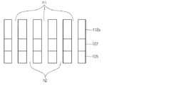
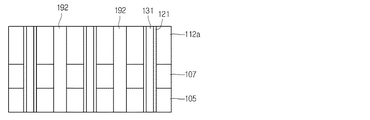
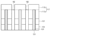
図1は、本発明の第1実施形態に従う発光素子100の断面図である。
105 基板
112 第1導電型半導体層
114 活性層
116 第2導電型半導体層
121 第1絶縁層
122 第2絶縁層
131 第1ビア電極
132 第2ビア電極
200 発光素子パッケージ
205 パッケージ胴体部
213 第3電極層
214 第4電極層
230 モールディング部材
2100 カバー
2200 光源モジュール
2300 部材
2400 放熱体
2500 ホルダー
2600 電源提供部
2700 内部ケース
2800 ソケット
Claims (20)
- 基板105と、
前記基板105の上に第1導電型半導体層112と、
前記第1導電型半導体層112の上に活性層114と、
前記活性層114の上に第2導電型半導体層116と、
前記基板105を貫通する第1ビアホールh1を通じて前記第1導電型半導体層112と接する第1ビア電極131と、
前記基板105、前記第1導電型半導体層112、前記活性層114を貫通する第2ビアホールh2を通じて前記第2導電型半導体層116と接する第2ビア電極132と、
を含むことを特徴とする、発光素子。 - 前記第1ビア電極131の側面を覆いかぶせる第1絶縁層121をさらに含むことを特徴とする、請求項1に記載の発光素子。
- 前記第1ビア電極131は、窒化物遷移金属を含むことを特徴とする、請求項1または2に記載の発光素子。
- 前記第1ビア電極131は、CrN、TiN、CrAlNのうち、いずれか1つ以上を含むことを特徴とする、請求項1乃至3のうち、いずれか1項に記載の発光素子。
- 前記第1ビア電極131は、融点が1500℃以上の窒化物遷移金属を含むことを特徴とする、請求項1乃至4のうち、いずれか1項に記載の発光素子。
- 前記第1ビア電極131は、光透光性が70%以上の窒化物遷移金属を含むことを特徴とする、請求項1乃至5のうち、いずれか1項に記載の発光素子。
- 前記第1ビア電極131は、電気抵抗が70[μΩcm]以下の窒化物遷移金属を含むことを特徴とする、請求項1乃至6のうち、いずれか1項に記載の発光素子。
- 前記第1ビア電極131の上面と接しながら前記第1ビア電極131から延びる第1延長電極133をさらに含むことを特徴とする、請求項1乃至7のうち、いずれか1項に記載の発光素子。
- 前記第2ビア電極132の上面と接しながら前記第2ビア電極132から延びる第2延長電極134をさらに含むことを特徴とする、請求項1乃至8のうち、いずれか1項に記載の発光素子。
- 前記第2ビア電極132の側面を覆いかぶせる第2絶縁層122をさらに含むことを特徴とする、請求項1乃至9のうち、いずれか1項に記載の発光素子。
- 前記第2ビア電極132は窒化物遷移金属を含むことを特徴とする、請求項1乃至10のうち、いずれか1項に記載の発光素子。
- 前記第2ビア電極132は、CrN、TiN、CrAlNのうち、いずれか1つ以上を含むことを特徴とする、請求項1乃至11のうち、いずれか1項に記載の発光素子。
- 前記第2ビア電極132は、融点が1500℃以上の窒化物遷移金属を含むことを特徴とする、請求項1乃至12のうち、いずれか1項に記載の発光素子。
- 前記第1ビア電極132は、光透光性が70%以上の窒化物遷移金属を含むことを特徴とする、請求項1乃至13のうち、いずれか1項に記載の発光素子。
- 前記第2ビア電極132は、電気抵抗が70[μΩcm]以下の窒化物遷移金属を含むことを特徴とする、請求項1乃至14のうち、いずれか1項に記載の発光素子。
- 前記第1ビアホールh1は底面から前記基板105を貫通し、
前記第1ビア電極131が前記第1ビアホールh1を通じて前記第1導電型半導体層112の底面と接することを特徴とする、請求項1乃至15のうち、いずれか1項に記載の発光素子。 - 前記第2ビアホールh2は底面から前記基板105、前記第1導電型半導体層112、及び前記活性層114を貫通し、
前記第2ビア電極132は、前記第2ビアホールh2を通じて前記第2導電型半導体層116の底面と接することを特徴とする、請求項1乃至16のうち、いずれか1項に記載の発光素子。 - 前記第2延長電極134は、前記第2ビア電極132の一側方向に延びることを特徴とする、請求項9に記載の発光素子。
- 前記第2延長電極134は、前記第2ビア電極132の長手方向と水平な方向に延びることを特徴とする、請求項9または18に記載の発光素子。
- 前記第2延長電極134bは、前記第2ビア電極132の両側方向に延びることを特徴とする、請求項9または19に記載の発光素子。
Applications Claiming Priority (2)
| Application Number | Priority Date | Filing Date | Title |
|---|---|---|---|
| KR10-2012-0115802 | 2012-10-18 | ||
| KR1020120115802A KR101979944B1 (ko) | 2012-10-18 | 2012-10-18 | 발광소자 |
Publications (2)
| Publication Number | Publication Date |
|---|---|
| JP2014086728A true JP2014086728A (ja) | 2014-05-12 |
| JP2014086728A5 JP2014086728A5 (ja) | 2016-11-10 |
Family
ID=49378167
Family Applications (1)
| Application Number | Title | Priority Date | Filing Date |
|---|---|---|---|
| JP2013217084A Pending JP2014086728A (ja) | 2012-10-18 | 2013-10-18 | 発光素子 |
Country Status (5)
| Country | Link |
|---|---|
| US (1) | US9660160B2 (ja) |
| EP (1) | EP2722899B1 (ja) |
| JP (1) | JP2014086728A (ja) |
| KR (1) | KR101979944B1 (ja) |
| CN (1) | CN103779471B (ja) |
Cited By (4)
| Publication number | Priority date | Publication date | Assignee | Title |
|---|---|---|---|---|
| WO2020100293A1 (ja) * | 2018-11-16 | 2020-05-22 | 堺ディスプレイプロダクト株式会社 | マイクロledデバイスおよびその製造方法 |
| WO2020100295A1 (ja) * | 2018-11-16 | 2020-05-22 | 堺ディスプレイプロダクト株式会社 | マイクロledデバイスおよびその製造方法 |
| WO2020100292A1 (ja) * | 2018-11-16 | 2020-05-22 | 堺ディスプレイプロダクト株式会社 | マイクロledデバイスおよびその製造方法 |
| WO2020115851A1 (ja) * | 2018-12-06 | 2020-06-11 | 堺ディスプレイプロダクト株式会社 | マイクロledデバイスおよびその製造方法 |
Families Citing this family (10)
| Publication number | Priority date | Publication date | Assignee | Title |
|---|---|---|---|---|
| CN104576862B (zh) * | 2014-12-24 | 2017-08-25 | 江苏巨晶新材料科技有限公司 | 一种基于铜衬底的氮化物led垂直芯片及其制备方法 |
| KR102419272B1 (ko) * | 2017-12-19 | 2022-07-11 | 엘지디스플레이 주식회사 | 발광 사운드 소자, 사운드 출력 장치 및 디스플레이 장치 |
| CN108281540B (zh) * | 2018-01-26 | 2020-05-22 | 扬州乾照光电有限公司 | 一种热电分流垂直结构led芯片及其制作方法 |
| JP7369136B2 (ja) * | 2018-03-26 | 2023-10-25 | ローレンス・リバモア・ナショナル・セキュリティ・エルエルシー | 設計された電流密度プロファイル・ダイオードレーザ |
| KR102097865B1 (ko) * | 2018-05-04 | 2020-05-27 | 고려대학교 산학협력단 | 발광소자 |
| CN111801806B (zh) * | 2018-07-09 | 2024-04-09 | 首尔伟傲世有限公司 | 发光元件及该发光元件的制造方法 |
| CN110265520A (zh) * | 2019-07-02 | 2019-09-20 | 华南理工大学 | 优化电流分布的嵌入式电极结构led芯片及其制备方法 |
| KR102174004B1 (ko) * | 2020-03-31 | 2020-11-04 | 고려대학교 산학협력단 | 발광소자 |
| CN113363365B (zh) * | 2021-08-09 | 2021-11-05 | 南昌凯捷半导体科技有限公司 | 一种多电流通道倒装AlGaInPmini-LED芯片及其制备方法 |
| CN116314508A (zh) * | 2023-05-22 | 2023-06-23 | 江西兆驰半导体有限公司 | 一种高光效led外延片及其制备方法、led芯片 |
Citations (13)
| Publication number | Priority date | Publication date | Assignee | Title |
|---|---|---|---|---|
| JPH0536346A (ja) * | 1991-07-31 | 1993-02-12 | Sony Corp | 金属製フイールドエミツタの作製方法 |
| JPH10270802A (ja) * | 1997-03-25 | 1998-10-09 | Sharp Corp | 窒化物系iii−v族化合物半導体装置及びその製造方法 |
| JPH11246289A (ja) * | 1998-03-02 | 1999-09-14 | Tokuyama Corp | メタライズされた窒化アルミニウム基板の製造方法 |
| JP2001176967A (ja) * | 1999-12-21 | 2001-06-29 | Nec Corp | 半導体装置及びその製造方法 |
| JP2001196633A (ja) * | 2000-01-05 | 2001-07-19 | Ind Technol Res Inst | 窒化ガリウムを基礎とする13族−15族化合物半導体素子および素子用電極 |
| JP2002341164A (ja) * | 2001-04-30 | 2002-11-27 | Agilent Technol Inc | 2次元フォトニック結晶スラブ導波路 |
| JP2009519608A (ja) * | 2005-12-16 | 2009-05-14 | サムスン エレクトロニクス カンパニー リミテッド | 光学素子およびその製造方法 |
| JP2009130047A (ja) * | 2007-11-21 | 2009-06-11 | Sharp Corp | 窒化物半導体用電極および窒化物半導体装置 |
| JP2010144248A (ja) * | 2008-12-22 | 2010-07-01 | Korea Advanced Inst Of Science & Technology | 窒化物/タングステンナノ複合粉末の製造方法及びその方法によって製造された窒化物/タングステンナノ複合粉末 |
| JP2010153870A (ja) * | 2008-12-24 | 2010-07-08 | Lg Innotek Co Ltd | 半導体発光素子 |
| JP2011029548A (ja) * | 2009-07-29 | 2011-02-10 | Mitsubishi Electric Corp | 電磁波透過性加飾部品 |
| JP2011060996A (ja) * | 2009-09-10 | 2011-03-24 | Napura:Kk | 発光ダイオード、発光装置、照明装置、ディスプレイ及び信号灯 |
| JP2011211189A (ja) * | 2010-03-26 | 2011-10-20 | Taiwan Semiconductor Manufacturing Co Ltd | 白色光、又は、カラー光を生成する光素子 |
Family Cites Families (10)
| Publication number | Priority date | Publication date | Assignee | Title |
|---|---|---|---|---|
| US7233028B2 (en) * | 2001-02-23 | 2007-06-19 | Nitronex Corporation | Gallium nitride material devices and methods of forming the same |
| US6611002B2 (en) | 2001-02-23 | 2003-08-26 | Nitronex Corporation | Gallium nitride material devices and methods including backside vias |
| TWI270222B (en) * | 2005-10-07 | 2007-01-01 | Formosa Epitaxy Inc | Light emitting diode chip |
| CN100446288C (zh) * | 2006-08-01 | 2008-12-24 | 金芃 | 通孔垂直结构的半导体芯片及其制造方法 |
| KR20110008550A (ko) * | 2009-07-20 | 2011-01-27 | 삼성전자주식회사 | 발광 소자 및 그 제조 방법 |
| US8198107B2 (en) * | 2009-10-07 | 2012-06-12 | Edison Opto Corporation | Method for manufacturing light emitting diode assembly |
| US20110198609A1 (en) * | 2010-02-12 | 2011-08-18 | Taiwan Semiconductor Manufacturing Company, Ltd. | Light-Emitting Devices with Through-Substrate Via Connections |
| KR101028327B1 (ko) | 2010-04-15 | 2011-04-12 | 엘지이노텍 주식회사 | 발광소자, 발광소자 제조방법 및 발광소자 패키지 |
| US20120241718A1 (en) | 2011-03-21 | 2012-09-27 | Walsin Lihwa Corporation | High performance light emitting diode |
| US8344392B2 (en) * | 2011-05-12 | 2013-01-01 | Epistar Corporation | Light-emitting element and the manufacturing method thereof |
-
2012
- 2012-10-18 KR KR1020120115802A patent/KR101979944B1/ko active IP Right Grant
-
2013
- 2013-10-17 EP EP13189140.0A patent/EP2722899B1/en active Active
- 2013-10-17 US US14/056,211 patent/US9660160B2/en active Active
- 2013-10-18 CN CN201310491634.7A patent/CN103779471B/zh active Active
- 2013-10-18 JP JP2013217084A patent/JP2014086728A/ja active Pending
Patent Citations (13)
| Publication number | Priority date | Publication date | Assignee | Title |
|---|---|---|---|---|
| JPH0536346A (ja) * | 1991-07-31 | 1993-02-12 | Sony Corp | 金属製フイールドエミツタの作製方法 |
| JPH10270802A (ja) * | 1997-03-25 | 1998-10-09 | Sharp Corp | 窒化物系iii−v族化合物半導体装置及びその製造方法 |
| JPH11246289A (ja) * | 1998-03-02 | 1999-09-14 | Tokuyama Corp | メタライズされた窒化アルミニウム基板の製造方法 |
| JP2001176967A (ja) * | 1999-12-21 | 2001-06-29 | Nec Corp | 半導体装置及びその製造方法 |
| JP2001196633A (ja) * | 2000-01-05 | 2001-07-19 | Ind Technol Res Inst | 窒化ガリウムを基礎とする13族−15族化合物半導体素子および素子用電極 |
| JP2002341164A (ja) * | 2001-04-30 | 2002-11-27 | Agilent Technol Inc | 2次元フォトニック結晶スラブ導波路 |
| JP2009519608A (ja) * | 2005-12-16 | 2009-05-14 | サムスン エレクトロニクス カンパニー リミテッド | 光学素子およびその製造方法 |
| JP2009130047A (ja) * | 2007-11-21 | 2009-06-11 | Sharp Corp | 窒化物半導体用電極および窒化物半導体装置 |
| JP2010144248A (ja) * | 2008-12-22 | 2010-07-01 | Korea Advanced Inst Of Science & Technology | 窒化物/タングステンナノ複合粉末の製造方法及びその方法によって製造された窒化物/タングステンナノ複合粉末 |
| JP2010153870A (ja) * | 2008-12-24 | 2010-07-08 | Lg Innotek Co Ltd | 半導体発光素子 |
| JP2011029548A (ja) * | 2009-07-29 | 2011-02-10 | Mitsubishi Electric Corp | 電磁波透過性加飾部品 |
| JP2011060996A (ja) * | 2009-09-10 | 2011-03-24 | Napura:Kk | 発光ダイオード、発光装置、照明装置、ディスプレイ及び信号灯 |
| JP2011211189A (ja) * | 2010-03-26 | 2011-10-20 | Taiwan Semiconductor Manufacturing Co Ltd | 白色光、又は、カラー光を生成する光素子 |
Cited By (7)
| Publication number | Priority date | Publication date | Assignee | Title |
|---|---|---|---|---|
| WO2020100293A1 (ja) * | 2018-11-16 | 2020-05-22 | 堺ディスプレイプロダクト株式会社 | マイクロledデバイスおよびその製造方法 |
| WO2020100295A1 (ja) * | 2018-11-16 | 2020-05-22 | 堺ディスプレイプロダクト株式会社 | マイクロledデバイスおよびその製造方法 |
| WO2020100292A1 (ja) * | 2018-11-16 | 2020-05-22 | 堺ディスプレイプロダクト株式会社 | マイクロledデバイスおよびその製造方法 |
| JPWO2020100293A1 (ja) * | 2018-11-16 | 2021-09-24 | 堺ディスプレイプロダクト株式会社 | マイクロledデバイスおよびその製造方法 |
| JPWO2020100295A1 (ja) * | 2018-11-16 | 2021-10-07 | 堺ディスプレイプロダクト株式会社 | マイクロledデバイスおよびその製造方法 |
| WO2020115851A1 (ja) * | 2018-12-06 | 2020-06-11 | 堺ディスプレイプロダクト株式会社 | マイクロledデバイスおよびその製造方法 |
| JPWO2020115851A1 (ja) * | 2018-12-06 | 2021-10-14 | 堺ディスプレイプロダクト株式会社 | マイクロledデバイスおよびその製造方法 |
Also Published As
| Publication number | Publication date |
|---|---|
| EP2722899A3 (en) | 2015-11-18 |
| KR101979944B1 (ko) | 2019-05-17 |
| EP2722899A2 (en) | 2014-04-23 |
| KR20140049689A (ko) | 2014-04-28 |
| CN103779471B (zh) | 2017-03-01 |
| US9660160B2 (en) | 2017-05-23 |
| US20140110742A1 (en) | 2014-04-24 |
| EP2722899B1 (en) | 2018-07-25 |
| CN103779471A (zh) | 2014-05-07 |
Similar Documents
| Publication | Publication Date | Title |
|---|---|---|
| KR101979944B1 (ko) | 발광소자 | |
| KR101953716B1 (ko) | 발광소자, 발광 소자 패키지 및 조명 시스템 | |
| KR101154709B1 (ko) | 발광 소자, 발광 소자 제조방법, 발광 소자 패키지 및 조명 시스템 | |
| KR102175345B1 (ko) | 발광소자 및 조명시스템 | |
| KR20160054712A (ko) | 반도체 발광소자 및 반도체 발광소자 패키지 | |
| KR20140062945A (ko) | 발광소자 | |
| KR102019858B1 (ko) | 발광소자 및 조명시스템 | |
| KR102163956B1 (ko) | 발광소자 및 조명시스템 | |
| KR102075749B1 (ko) | 발광소자 패키지 | |
| KR20110129620A (ko) | 발광 소자, 발광 소자 제조방법 및 발광 소자 패키지 | |
| KR101973608B1 (ko) | 발광소자 | |
| KR102200000B1 (ko) | 발광소자 및 조명시스템 | |
| US10008633B2 (en) | Light-emitting diode and lighting system | |
| KR102181404B1 (ko) | 발광소자 및 조명시스템 | |
| KR102181429B1 (ko) | 발광소자 및 조명시스템 | |
| KR102200005B1 (ko) | 발광소자 | |
| KR20150061844A (ko) | 발광소자 및 조명장치 | |
| KR102199998B1 (ko) | 발광소자 | |
| KR102153125B1 (ko) | 발광소자 및 조명시스템 | |
| KR20140078250A (ko) | 발광소자, 발광 소자 제조방법 및 조명 시스템 | |
| KR101734544B1 (ko) | 발광소자 패키지 | |
| KR102175315B1 (ko) | 발광소자 및 조명시스템 | |
| KR102109131B1 (ko) | 발광소자 및 조명시스템 | |
| KR102224086B1 (ko) | 발광소자 및 조명시스템 | |
| KR102187514B1 (ko) | 발광소자 |
Legal Events
| Date | Code | Title | Description |
|---|---|---|---|
| A521 | Request for written amendment filed |
Free format text: JAPANESE INTERMEDIATE CODE: A523 Effective date: 20160923 |
|
| A621 | Written request for application examination |
Free format text: JAPANESE INTERMEDIATE CODE: A621 Effective date: 20160923 |
|
| A977 | Report on retrieval |
Free format text: JAPANESE INTERMEDIATE CODE: A971007 Effective date: 20170825 |
|
| A131 | Notification of reasons for refusal |
Free format text: JAPANESE INTERMEDIATE CODE: A131 Effective date: 20170905 |
|
| A521 | Request for written amendment filed |
Free format text: JAPANESE INTERMEDIATE CODE: A523 Effective date: 20171129 |
|
| A02 | Decision of refusal |
Free format text: JAPANESE INTERMEDIATE CODE: A02 Effective date: 20180508 |