JP2013247132A - 板状物の加工方法 - Google Patents
板状物の加工方法 Download PDFInfo
- Publication number
- JP2013247132A JP2013247132A JP2012117519A JP2012117519A JP2013247132A JP 2013247132 A JP2013247132 A JP 2013247132A JP 2012117519 A JP2012117519 A JP 2012117519A JP 2012117519 A JP2012117519 A JP 2012117519A JP 2013247132 A JP2013247132 A JP 2013247132A
- Authority
- JP
- Japan
- Prior art keywords
- plate
- polishing
- wafer
- polishing pad
- chuck table
- Prior art date
- Legal status (The legal status is an assumption and is not a legal conclusion. Google has not performed a legal analysis and makes no representation as to the accuracy of the status listed.)
- Granted
Links
- 238000000034 method Methods 0.000 title claims abstract description 12
- 238000005498 polishing Methods 0.000 claims abstract description 106
- 239000007788 liquid Substances 0.000 claims abstract description 56
- 238000005247 gettering Methods 0.000 claims abstract description 33
- 239000006061 abrasive grain Substances 0.000 claims abstract description 15
- XLYOFNOQVPJJNP-UHFFFAOYSA-N water Substances O XLYOFNOQVPJJNP-UHFFFAOYSA-N 0.000 claims description 12
- 239000000463 material Substances 0.000 claims description 10
- XUIMIQQOPSSXEZ-UHFFFAOYSA-N Silicon Chemical compound [Si] XUIMIQQOPSSXEZ-UHFFFAOYSA-N 0.000 claims description 9
- 238000003672 processing method Methods 0.000 claims description 9
- 229910052710 silicon Inorganic materials 0.000 claims description 9
- 239000010703 silicon Substances 0.000 claims description 9
- 230000002378 acidificating effect Effects 0.000 claims description 4
- 230000000694 effects Effects 0.000 abstract description 8
- 239000002253 acid Substances 0.000 abstract 1
- 235000012431 wafers Nutrition 0.000 description 99
- 239000004065 semiconductor Substances 0.000 description 24
- 238000004140 cleaning Methods 0.000 description 11
- 238000003754 machining Methods 0.000 description 8
- 239000012530 fluid Substances 0.000 description 5
- 238000006243 chemical reaction Methods 0.000 description 4
- 239000012535 impurity Substances 0.000 description 4
- 230000032258 transport Effects 0.000 description 4
- JOYRKODLDBILNP-UHFFFAOYSA-N Ethyl urethane Chemical compound CCOC(N)=O JOYRKODLDBILNP-UHFFFAOYSA-N 0.000 description 3
- 230000015572 biosynthetic process Effects 0.000 description 3
- 229910003460 diamond Inorganic materials 0.000 description 3
- 239000010432 diamond Substances 0.000 description 3
- 238000004519 manufacturing process Methods 0.000 description 3
- 239000000126 substance Substances 0.000 description 3
- 239000000758 substrate Substances 0.000 description 3
- JMASRVWKEDWRBT-UHFFFAOYSA-N Gallium nitride Chemical compound [Ga]#N JMASRVWKEDWRBT-UHFFFAOYSA-N 0.000 description 2
- 239000007864 aqueous solution Substances 0.000 description 2
- 239000013078 crystal Substances 0.000 description 2
- 230000007547 defect Effects 0.000 description 2
- 239000006260 foam Substances 0.000 description 2
- 239000011521 glass Substances 0.000 description 2
- 230000003287 optical effect Effects 0.000 description 2
- 230000002093 peripheral effect Effects 0.000 description 2
- 239000004094 surface-active agent Substances 0.000 description 2
- 229910052582 BN Inorganic materials 0.000 description 1
- PZNSFCLAULLKQX-UHFFFAOYSA-N Boron nitride Chemical compound N#B PZNSFCLAULLKQX-UHFFFAOYSA-N 0.000 description 1
- 239000012670 alkaline solution Substances 0.000 description 1
- PNEYBMLMFCGWSK-UHFFFAOYSA-N aluminium oxide Inorganic materials [O-2].[O-2].[O-2].[Al+3].[Al+3] PNEYBMLMFCGWSK-UHFFFAOYSA-N 0.000 description 1
- 238000005452 bending Methods 0.000 description 1
- 239000007767 bonding agent Substances 0.000 description 1
- 239000000919 ceramic Substances 0.000 description 1
- CETPSERCERDGAM-UHFFFAOYSA-N ceric oxide Chemical compound O=[Ce]=O CETPSERCERDGAM-UHFFFAOYSA-N 0.000 description 1
- 229910000422 cerium(IV) oxide Inorganic materials 0.000 description 1
- 238000011109 contamination Methods 0.000 description 1
- 230000006866 deterioration Effects 0.000 description 1
- 238000007599 discharging Methods 0.000 description 1
- 229910001385 heavy metal Inorganic materials 0.000 description 1
- 238000005259 measurement Methods 0.000 description 1
- 239000004745 nonwoven fabric Substances 0.000 description 1
- 239000002245 particle Substances 0.000 description 1
- 230000001681 protective effect Effects 0.000 description 1
- 238000006748 scratching Methods 0.000 description 1
- 230000002393 scratching effect Effects 0.000 description 1
- 239000002699 waste material Substances 0.000 description 1
Images


Landscapes
- Mechanical Treatment Of Semiconductor (AREA)
Abstract
【解決手段】 板状物の加工方法であって、板状物をチャックテーブルで保持する保持ステップと、板状物を保持した該チャックテーブルを回転させつつ、砥粒を含有する研磨パッドを回転させて該チャックテーブルに保持された板状物を押圧するとともにアルカリ性又は酸性の研磨液を板状物と該研磨パッドとに供給しながら、該研磨パッドで板状物を研磨する研磨ステップと、該研磨ステップを実施した後、該チャックテーブルと該研磨パッドとを回転させるとともに該チャックテーブルに保持された板状物と板状物を押圧する該研磨パッドとにリンス液を供給しながら、該研磨パッドで板状物にゲッタリング層を生成するゲッタリング層生成ステップと、を備えたことを特徴とする。
【選択図】図7
Description
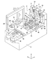
12 粗研削ユニット
15 デバイス
16 仕上げ研削ユニット
23 表面保護テープ
48 ターンテーブル
50 チャックテーブル
52 研磨ユニット
74 研磨パッド
78 加工液供給ノズル
80 電磁切替弁
82 研磨液供給源
84 リンス液供給源
Claims (2)
- 板状物の加工方法であって、
板状物をチャックテーブルで保持する保持ステップと、
板状物を保持した該チャックテーブルを回転させつつ、砥粒を含有する研磨パッドを回転させて該チャックテーブルに保持された板状物を押圧するとともにアルカリ性又は酸性の研磨液を板状物と該研磨パッドとに供給しながら、該研磨パッドで板状物を研磨する研磨ステップと、
該研磨ステップを実施した後、該チャックテーブルと該研磨パッドとを回転させるとともに該チャックテーブルに保持された板状物と板状物を押圧する該研磨パッドとにリンス液を供給しながら、該研磨パッドで板状物にゲッタリング層を生成するゲッタリング層生成ステップと、
を備えたことを特徴とする板状物の加工方法。 - 前記板状物はシリコンウエーハから構成され、
前記研磨液はアルカリ性であり、前記リンス液は純水である請求項1記載の板状物の加工方法。
Priority Applications (1)
| Application Number | Priority Date | Filing Date | Title |
|---|---|---|---|
| JP2012117519A JP5963537B2 (ja) | 2012-05-23 | 2012-05-23 | シリコンウエーハの加工方法 |
Applications Claiming Priority (1)
| Application Number | Priority Date | Filing Date | Title |
|---|---|---|---|
| JP2012117519A JP5963537B2 (ja) | 2012-05-23 | 2012-05-23 | シリコンウエーハの加工方法 |
Related Child Applications (1)
| Application Number | Title | Priority Date | Filing Date |
|---|---|---|---|
| JP2016135040A Division JP6192778B2 (ja) | 2016-07-07 | 2016-07-07 | シリコンウエーハの加工装置 |
Publications (2)
| Publication Number | Publication Date |
|---|---|
| JP2013247132A true JP2013247132A (ja) | 2013-12-09 |
| JP5963537B2 JP5963537B2 (ja) | 2016-08-03 |
Family
ID=49846712
Family Applications (1)
| Application Number | Title | Priority Date | Filing Date |
|---|---|---|---|
| JP2012117519A Active JP5963537B2 (ja) | 2012-05-23 | 2012-05-23 | シリコンウエーハの加工方法 |
Country Status (1)
| Country | Link |
|---|---|
| JP (1) | JP5963537B2 (ja) |
Cited By (9)
| Publication number | Priority date | Publication date | Assignee | Title |
|---|---|---|---|---|
| JP2018056459A (ja) * | 2016-09-30 | 2018-04-05 | 株式会社ディスコ | ウエーハの加工方法 |
| CN107887266A (zh) * | 2016-09-29 | 2018-04-06 | 株式会社迪思科 | 器件晶片的加工方法 |
| CN107891358A (zh) * | 2016-10-03 | 2018-04-10 | 株式会社迪思科 | 晶片的加工方法和研磨装置 |
| KR20180037123A (ko) * | 2016-10-03 | 2018-04-11 | 가부시기가이샤 디스코 | 웨이퍼의 가공 방법 |
| KR20180057545A (ko) | 2016-11-22 | 2018-05-30 | 가부시기가이샤 디스코 | 웨이퍼의 가공 방법 |
| JP2018190812A (ja) * | 2017-05-01 | 2018-11-29 | 株式会社ディスコ | ウエーハの加工方法 |
| WO2018221290A1 (ja) * | 2017-06-01 | 2018-12-06 | 東京エレクトロン株式会社 | ゲッタリング層形成装置、ゲッタリング層形成方法及びコンピュータ記憶媒体 |
| JP2019021695A (ja) * | 2017-07-13 | 2019-02-07 | 株式会社ディスコ | ウエーハの加工方法 |
| CN110355682A (zh) * | 2018-04-05 | 2019-10-22 | 株式会社迪思科 | SiC基板的研磨方法 |
Citations (6)
| Publication number | Priority date | Publication date | Assignee | Title |
|---|---|---|---|---|
| US20040011991A1 (en) * | 2001-06-13 | 2004-01-22 | Markle Richard J. | Use of a gettering agent in a chemical mechanical polishing and rinsing operation and apparatus therefor |
| JP2006319249A (ja) * | 2005-05-16 | 2006-11-24 | Nikon Corp | 研磨装置、この研磨装置を用いた半導体デバイス製造方法及びこの製造方法により製造された半導体デバイス |
| JP2007242902A (ja) * | 2006-03-09 | 2007-09-20 | Disco Abrasive Syst Ltd | ウエーハの加工方法 |
| JP2009081475A (ja) * | 2009-01-22 | 2009-04-16 | Fujitsu Microelectronics Ltd | 半導体装置の製造方法 |
| JP2011101913A (ja) * | 2009-11-10 | 2011-05-26 | Disco Abrasive Syst Ltd | ウエーハの加工装置 |
| JP2011167818A (ja) * | 2010-02-19 | 2011-09-01 | Disco Corp | 加工装置 |
-
2012
- 2012-05-23 JP JP2012117519A patent/JP5963537B2/ja active Active
Patent Citations (6)
| Publication number | Priority date | Publication date | Assignee | Title |
|---|---|---|---|---|
| US20040011991A1 (en) * | 2001-06-13 | 2004-01-22 | Markle Richard J. | Use of a gettering agent in a chemical mechanical polishing and rinsing operation and apparatus therefor |
| JP2006319249A (ja) * | 2005-05-16 | 2006-11-24 | Nikon Corp | 研磨装置、この研磨装置を用いた半導体デバイス製造方法及びこの製造方法により製造された半導体デバイス |
| JP2007242902A (ja) * | 2006-03-09 | 2007-09-20 | Disco Abrasive Syst Ltd | ウエーハの加工方法 |
| JP2009081475A (ja) * | 2009-01-22 | 2009-04-16 | Fujitsu Microelectronics Ltd | 半導体装置の製造方法 |
| JP2011101913A (ja) * | 2009-11-10 | 2011-05-26 | Disco Abrasive Syst Ltd | ウエーハの加工装置 |
| JP2011167818A (ja) * | 2010-02-19 | 2011-09-01 | Disco Corp | 加工装置 |
Cited By (23)
| Publication number | Priority date | Publication date | Assignee | Title |
|---|---|---|---|---|
| CN107887266A (zh) * | 2016-09-29 | 2018-04-06 | 株式会社迪思科 | 器件晶片的加工方法 |
| JP2018056459A (ja) * | 2016-09-30 | 2018-04-05 | 株式会社ディスコ | ウエーハの加工方法 |
| JP2018060872A (ja) * | 2016-10-03 | 2018-04-12 | 株式会社ディスコ | ウエーハの加工方法及び研磨装置 |
| KR20180037123A (ko) * | 2016-10-03 | 2018-04-11 | 가부시기가이샤 디스코 | 웨이퍼의 가공 방법 |
| KR20180037113A (ko) * | 2016-10-03 | 2018-04-11 | 가부시기가이샤 디스코 | 웨이퍼의 가공 방법 및 연마 장치 |
| JP2018060873A (ja) * | 2016-10-03 | 2018-04-12 | 株式会社ディスコ | ウエーハの加工方法 |
| TWI727089B (zh) * | 2016-10-03 | 2021-05-11 | 日商迪思科股份有限公司 | 晶圓的加工方法及研磨裝置 |
| CN107891358A (zh) * | 2016-10-03 | 2018-04-10 | 株式会社迪思科 | 晶片的加工方法和研磨装置 |
| KR102320761B1 (ko) * | 2016-10-03 | 2021-11-01 | 가부시기가이샤 디스코 | 웨이퍼의 가공 방법 및 연마 장치 |
| KR102255728B1 (ko) * | 2016-10-03 | 2021-05-26 | 가부시기가이샤 디스코 | 웨이퍼의 가공 방법 |
| KR20180057545A (ko) | 2016-11-22 | 2018-05-30 | 가부시기가이샤 디스코 | 웨이퍼의 가공 방법 |
| JP2018085411A (ja) * | 2016-11-22 | 2018-05-31 | 株式会社ディスコ | ウエーハの加工方法 |
| KR102282258B1 (ko) | 2016-11-22 | 2021-07-26 | 가부시기가이샤 디스코 | 웨이퍼의 가공 방법 |
| JP2018190812A (ja) * | 2017-05-01 | 2018-11-29 | 株式会社ディスコ | ウエーハの加工方法 |
| WO2018221290A1 (ja) * | 2017-06-01 | 2018-12-06 | 東京エレクトロン株式会社 | ゲッタリング層形成装置、ゲッタリング層形成方法及びコンピュータ記憶媒体 |
| JPWO2018221290A1 (ja) * | 2017-06-01 | 2020-03-26 | 東京エレクトロン株式会社 | ゲッタリング層形成装置、ゲッタリング層形成方法及びコンピュータ記憶媒体 |
| CN110692124A (zh) * | 2017-06-01 | 2020-01-14 | 东京毅力科创株式会社 | 吸杂层形成装置、吸杂层形成方法以及计算机存储介质 |
| TWI812622B (zh) * | 2017-06-01 | 2023-08-21 | 日商東京威力科創股份有限公司 | 吸集層形成裝置、吸集層形成方法及電腦記錄媒體 |
| JP2019021695A (ja) * | 2017-07-13 | 2019-02-07 | 株式会社ディスコ | ウエーハの加工方法 |
| JP2019186323A (ja) * | 2018-04-05 | 2019-10-24 | 株式会社ディスコ | SiC基板の研磨方法 |
| CN110355682A (zh) * | 2018-04-05 | 2019-10-22 | 株式会社迪思科 | SiC基板的研磨方法 |
| JP7106209B2 (ja) | 2018-04-05 | 2022-07-26 | 株式会社ディスコ | SiC基板の研磨方法 |
| TWI802673B (zh) * | 2018-04-05 | 2023-05-21 | 日商迪思科股份有限公司 | SiC基板的研磨方法 |
Also Published As
| Publication number | Publication date |
|---|---|
| JP5963537B2 (ja) | 2016-08-03 |
Similar Documents
| Publication | Publication Date | Title |
|---|---|---|
| JP5916513B2 (ja) | 板状物の加工方法 | |
| JP5963537B2 (ja) | シリコンウエーハの加工方法 | |
| JP5406676B2 (ja) | ウエーハの加工装置 | |
| JP6192778B2 (ja) | シリコンウエーハの加工装置 | |
| JP6723892B2 (ja) | ウエーハの加工方法 | |
| TW201824392A (zh) | 加工裝置 | |
| JP5410940B2 (ja) | 研削装置 | |
| TWI727089B (zh) | 晶圓的加工方法及研磨裝置 | |
| JP5466963B2 (ja) | 研削装置 | |
| JP5907797B2 (ja) | ウエーハの加工方法 | |
| JP6851761B2 (ja) | 板状物の加工方法 | |
| JP2008109006A (ja) | ウエーハの研削方法 | |
| JP2011031359A (ja) | 研磨工具、研磨装置および研磨加工方法 | |
| JP5399829B2 (ja) | 研磨パッドのドレッシング方法 | |
| JP2016179533A (ja) | 被加工物の研削方法及び研削装置 | |
| US20200391337A1 (en) | Grinding apparatus and use method of grinding apparatus | |
| JP7118558B2 (ja) | 被加工物の加工方法 | |
| JP2016078132A (ja) | 加工装置 | |
| JP7301472B2 (ja) | ウェーハの加工方法 | |
| JP5973284B2 (ja) | 研削装置 | |
| TWI769294B (zh) | 研磨墊 | |
| JP7304708B2 (ja) | ウェーハの加工方法 | |
| JP2023104444A (ja) | 被加工物の加工方法 | |
| TW202324528A (zh) | 被加工物之磨削方法 | |
| JP2014079859A (ja) | 研削装置 |
Legal Events
| Date | Code | Title | Description |
|---|---|---|---|
| A621 | Written request for application examination |
Free format text: JAPANESE INTERMEDIATE CODE: A621 Effective date: 20150423 |
|
| A977 | Report on retrieval |
Free format text: JAPANESE INTERMEDIATE CODE: A971007 Effective date: 20160420 |
|
| A131 | Notification of reasons for refusal |
Free format text: JAPANESE INTERMEDIATE CODE: A131 Effective date: 20160426 |
|
| A521 | Request for written amendment filed |
Free format text: JAPANESE INTERMEDIATE CODE: A523 Effective date: 20160608 |
|
| TRDD | Decision of grant or rejection written | ||
| A01 | Written decision to grant a patent or to grant a registration (utility model) |
Free format text: JAPANESE INTERMEDIATE CODE: A01 Effective date: 20160628 |
|
| A61 | First payment of annual fees (during grant procedure) |
Free format text: JAPANESE INTERMEDIATE CODE: A61 Effective date: 20160628 |
|
| R150 | Certificate of patent or registration of utility model |
Ref document number: 5963537 Country of ref document: JP Free format text: JAPANESE INTERMEDIATE CODE: R150 |
|
| R250 | Receipt of annual fees |
Free format text: JAPANESE INTERMEDIATE CODE: R250 |
|
| R250 | Receipt of annual fees |
Free format text: JAPANESE INTERMEDIATE CODE: R250 |
|
| R250 | Receipt of annual fees |
Free format text: JAPANESE INTERMEDIATE CODE: R250 |
|
| R250 | Receipt of annual fees |
Free format text: JAPANESE INTERMEDIATE CODE: R250 |
|
| R250 | Receipt of annual fees |
Free format text: JAPANESE INTERMEDIATE CODE: R250 |