JP2013068837A - 表示装置およびその駆動方法、ならびに電子機器 - Google Patents
表示装置およびその駆動方法、ならびに電子機器 Download PDFInfo
- Publication number
- JP2013068837A JP2013068837A JP2011207986A JP2011207986A JP2013068837A JP 2013068837 A JP2013068837 A JP 2013068837A JP 2011207986 A JP2011207986 A JP 2011207986A JP 2011207986 A JP2011207986 A JP 2011207986A JP 2013068837 A JP2013068837 A JP 2013068837A
- Authority
- JP
- Japan
- Prior art keywords
- data
- pair
- data lines
- pixel
- potential
- Prior art date
- Legal status (The legal status is an assumption and is not a legal conclusion. Google has not performed a legal analysis and makes no representation as to the accuracy of the status listed.)
- Pending
Links
Images


Classifications
-
- G—PHYSICS
- G09—EDUCATION; CRYPTOGRAPHY; DISPLAY; ADVERTISING; SEALS
- G09G—ARRANGEMENTS OR CIRCUITS FOR CONTROL OF INDICATING DEVICES USING STATIC MEANS TO PRESENT VARIABLE INFORMATION
- G09G3/00—Control arrangements or circuits, of interest only in connection with visual indicators other than cathode-ray tubes
- G09G3/20—Control arrangements or circuits, of interest only in connection with visual indicators other than cathode-ray tubes for presentation of an assembly of a number of characters, e.g. a page, by composing the assembly by combination of individual elements arranged in a matrix no fixed position being assigned to or needed to be assigned to the individual characters or partial characters
- G09G3/34—Control arrangements or circuits, of interest only in connection with visual indicators other than cathode-ray tubes for presentation of an assembly of a number of characters, e.g. a page, by composing the assembly by combination of individual elements arranged in a matrix no fixed position being assigned to or needed to be assigned to the individual characters or partial characters by control of light from an independent source
- G09G3/36—Control arrangements or circuits, of interest only in connection with visual indicators other than cathode-ray tubes for presentation of an assembly of a number of characters, e.g. a page, by composing the assembly by combination of individual elements arranged in a matrix no fixed position being assigned to or needed to be assigned to the individual characters or partial characters by control of light from an independent source using liquid crystals
- G09G3/3611—Control of matrices with row and column drivers
- G09G3/3685—Details of drivers for data electrodes
-
- G—PHYSICS
- G09—EDUCATION; CRYPTOGRAPHY; DISPLAY; ADVERTISING; SEALS
- G09G—ARRANGEMENTS OR CIRCUITS FOR CONTROL OF INDICATING DEVICES USING STATIC MEANS TO PRESENT VARIABLE INFORMATION
- G09G3/00—Control arrangements or circuits, of interest only in connection with visual indicators other than cathode-ray tubes
- G09G3/20—Control arrangements or circuits, of interest only in connection with visual indicators other than cathode-ray tubes for presentation of an assembly of a number of characters, e.g. a page, by composing the assembly by combination of individual elements arranged in a matrix no fixed position being assigned to or needed to be assigned to the individual characters or partial characters
- G09G3/34—Control arrangements or circuits, of interest only in connection with visual indicators other than cathode-ray tubes for presentation of an assembly of a number of characters, e.g. a page, by composing the assembly by combination of individual elements arranged in a matrix no fixed position being assigned to or needed to be assigned to the individual characters or partial characters by control of light from an independent source
- G09G3/36—Control arrangements or circuits, of interest only in connection with visual indicators other than cathode-ray tubes for presentation of an assembly of a number of characters, e.g. a page, by composing the assembly by combination of individual elements arranged in a matrix no fixed position being assigned to or needed to be assigned to the individual characters or partial characters by control of light from an independent source using liquid crystals
- G09G3/3611—Control of matrices with row and column drivers
- G09G3/3648—Control of matrices with row and column drivers using an active matrix
-
- G—PHYSICS
- G09—EDUCATION; CRYPTOGRAPHY; DISPLAY; ADVERTISING; SEALS
- G09G—ARRANGEMENTS OR CIRCUITS FOR CONTROL OF INDICATING DEVICES USING STATIC MEANS TO PRESENT VARIABLE INFORMATION
- G09G5/00—Control arrangements or circuits for visual indicators common to cathode-ray tube indicators and other visual indicators
- G09G5/18—Timing circuits for raster scan displays
-
- G—PHYSICS
- G09—EDUCATION; CRYPTOGRAPHY; DISPLAY; ADVERTISING; SEALS
- G09G—ARRANGEMENTS OR CIRCUITS FOR CONTROL OF INDICATING DEVICES USING STATIC MEANS TO PRESENT VARIABLE INFORMATION
- G09G2300/00—Aspects of the constitution of display devices
- G09G2300/04—Structural and physical details of display devices
- G09G2300/0404—Matrix technologies
-
- G—PHYSICS
- G09—EDUCATION; CRYPTOGRAPHY; DISPLAY; ADVERTISING; SEALS
- G09G—ARRANGEMENTS OR CIRCUITS FOR CONTROL OF INDICATING DEVICES USING STATIC MEANS TO PRESENT VARIABLE INFORMATION
- G09G2310/00—Command of the display device
- G09G2310/02—Addressing, scanning or driving the display screen or processing steps related thereto
- G09G2310/0243—Details of the generation of driving signals
- G09G2310/0248—Precharge or discharge of column electrodes before or after applying exact column voltages
-
- G—PHYSICS
- G09—EDUCATION; CRYPTOGRAPHY; DISPLAY; ADVERTISING; SEALS
- G09G—ARRANGEMENTS OR CIRCUITS FOR CONTROL OF INDICATING DEVICES USING STATIC MEANS TO PRESENT VARIABLE INFORMATION
- G09G3/00—Control arrangements or circuits, of interest only in connection with visual indicators other than cathode-ray tubes
- G09G3/20—Control arrangements or circuits, of interest only in connection with visual indicators other than cathode-ray tubes for presentation of an assembly of a number of characters, e.g. a page, by composing the assembly by combination of individual elements arranged in a matrix no fixed position being assigned to or needed to be assigned to the individual characters or partial characters
- G09G3/34—Control arrangements or circuits, of interest only in connection with visual indicators other than cathode-ray tubes for presentation of an assembly of a number of characters, e.g. a page, by composing the assembly by combination of individual elements arranged in a matrix no fixed position being assigned to or needed to be assigned to the individual characters or partial characters by control of light from an independent source
- G09G3/36—Control arrangements or circuits, of interest only in connection with visual indicators other than cathode-ray tubes for presentation of an assembly of a number of characters, e.g. a page, by composing the assembly by combination of individual elements arranged in a matrix no fixed position being assigned to or needed to be assigned to the individual characters or partial characters by control of light from an independent source using liquid crystals
- G09G3/3611—Control of matrices with row and column drivers
- G09G3/3685—Details of drivers for data electrodes
- G09G3/3688—Details of drivers for data electrodes suitable for active matrices only
Abstract
【解決手段】複数の一対のデータ線のそれぞれに対して、一対のデータ線同士を短絡する短絡回路を設ける。画素に対して映像信号の書き込みを行う前に、一対のデータ線をハイインピーダンス状態とする。画素に対して前記映像信号の書き込みが行われる前に一旦、一対のデータ線同士を短絡回路によって短絡状態とし、一対のデータ線間の電位を正相の電位と逆相の電位との中間の電位にした後、短絡状態を解除して映像信号の書き込みを行う。
【選択図】図1
Description
[表示装置の構成]
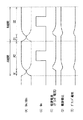
図1は、本開示の第1の実施の形態に係る表示装置の一構成例を示している。この表示装置は、データ線群とゲート線群とを備え、データ線群とゲート線群との各交点に画素111がマトリクス状に配置されて表示領域(表示部)10(破線領域内)を構成している。
図2は、画素11ごとの駆動回路の具体例を示している。ここでは、表示装置が、デジタル値で画素11への書き込みを行うパルス幅変調方式の液晶表示装置であるものとする。また、図2では一対のデータ線Dn/XDnとゲート線Gmとの交点に配置された画素11を代表して示している。この駆動回路は、画素電極21および対向電極22と、画素電極21と対向電極22との間に形成された液晶容量20とを備えている。画素電極21は例えば、複数の画素11に対応して図示しない画素基板上にマトリクス状に配置されている。対向電極22は例えば、複数の画素11に共通する電極として、図示しない対向基板上に配置されている。
(比較例に係る表示装置の動作)
まず、比較例として、短絡回路14を設けなかった場合の表示装置(図9参照)の動作およびその問題点について説明する。この比較例に係る表示装置の構成は、短絡回路14を設けていないことを除いて、図1および図2と同様の構成となっている。
上述の比較例を改善した、本実施の形態に係る表示装置の動作を、図3〜図4を参照して説明する。
以上説明したように、本実施の形態に係る表示装置によれば、データ線における電位変動を抑え、電位変動による画質の劣化の少ない表示を行うことができる。
図1の構成では短絡回路14をデータ駆動回路12側に配置していたが、図5に示すように、データ駆動回路12とは反対側に短絡回路14を配置しても良い。すなわち、表示領域10を挟んで、短絡回路14とデータ線駆動回路12とが互いに反対側に配置されていても良い。
次に、本開示の第2の実施の形態に係る表示装置について説明する。なお、上記第1の実施の形態に係る表示装置と実質的に同一の構成部分には同一の符号を付し、適宜説明を省略する。
図6の構成では短絡回路14をデータ駆動回路12側に配置していたが、図8に示すように、データ駆動回路12とは反対側に短絡回路14を配置しても良い。すなわち、表示領域10を挟んで、短絡回路14とデータ線駆動回路12とが互いに反対側に配置されていても良い。
本開示による技術は、上記各実施の形態の説明に限定されず種々の変形実施が可能である。
例えば、上記各実施の形態に係る表示装置はいずれも、表示機能を有する種々の電子機器に適用可能である。例えば、投射型のプロジェクタ、テレビジョン装置またはパーソナルコンピュータ等に適用可能である。
(1)
一対のデータ線が複数、第1の方向に並列的に配置されてなるデータ線群と、
ゲート線が複数、第2の方向に並列的に配置されてなるゲート線群と、
複数の画素を有し、前記各画素が前記一対のデータ線と前記ゲート線との交点に配置されてなる表示部と、
前記一対のデータ線の一方に正相のデータ信号を供給すると共に、前記一対のデータ線の他方に前記正相のデータ信号とは逆相のデータ信号を供給するデータ線駆動回路と、
前記ゲート線にゲート信号を供給するゲート線駆動回路と、
前記複数の一対のデータ線のそれぞれに対して設けられ、前記複数の一対のデータ線のそれぞれにおいて、前記一対のデータ線同士を短絡する短絡回路と
を備え、
前記画素は、前記一対のデータ線の少なくとも1つに接続され、前記正相のデータ信号と前記逆相のデータ信号との少なくとも1つのデータ信号が、映像信号として書き込まれるようになされ、
前記データ線駆動回路は、前記画素に対して前記映像信号の書き込みを行う前に、前記一対のデータ線をハイインピーダンス状態とし、
前記短絡回路は、前記画素に対して前記映像信号の書き込みが行われる前に一旦、前記一対のデータ線同士を短絡状態とし、前記一対のデータ線間の電位を正相の電位と逆相の電位との中間の電位にした後、前記短絡状態を解除して前記映像信号の書き込みが行われるようにする
表示装置。
(2)
前記画素は、前記一対のデータ線の両方に接続され、前記正相のデータ信号と前記逆相のデータ信号との差動による映像信号の書き込みが行われる
上記(1)に記載の表示装置。
(3)
前記画素が前記第2の方向に複数配置され、
前記複数の画素は、前記第2の方向において1画素ごとに前記一対のデータ線の一方と他方とに交互に接続され、前記第2の方向において1画素ごとに前記正相のデータ信号と前記逆相のデータ信号とが交互に前記映像信号として書き込まれる
上記(1)に記載の表示装置。
(4)
前記短絡回路が、前記表示部と前記データ線駆動回路との間に配置されている
上記(1)ないし(3)のいずれか1つに記載の表示装置。
(5)
前記表示部を挟んで、前記短絡回路と前記データ線駆動回路とが互いに反対側に配置されている
上記(1)ないし(3)のいずれか1つに記載の表示装置。
(6)
一対のデータ線が複数、第1の方向に並列的に配置されてなるデータ線群と、
ゲート線が複数、第2の方向に並列的に配置されてなるゲート線群と、
複数の画素を有し、前記各画素が前記一対のデータ線と前記ゲート線との交点に配置されてなる表示部と、
前記一対のデータ線の一方に正相のデータ信号を供給すると共に、前記一対のデータ線の他方に前記正相のデータ信号とは逆相のデータ信号を供給するデータ線駆動回路と、
前記ゲート線にゲート信号を供給するゲート線駆動回路と
を備え、
前記画素が、前記一対のデータ線の少なくとも1つに接続され、前記正相のデータ信号と前記逆相のデータ信号との少なくとも1つのデータ信号が、映像信号として書き込まれるようになされた表示装置に対して、
前記複数の一対のデータ線のそれぞれに対して、前記一対のデータ線同士を短絡する短絡回路を設け、
前記画素に対して前記映像信号の書き込みを行う前に、前記一対のデータ線をハイインピーダンス状態とし、
前記画素に対して前記映像信号の書き込みが行われる前に一旦、前記一対のデータ線同士を前記短絡回路によって短絡状態とし、前記一対のデータ線間の電位を正相の電位と逆相の電位との中間の電位にした後、前記短絡状態を解除して前記映像信号の書き込みを行う
表示装置の駆動方法。
(7)
表示装置を備え、
前記表示装置は、
一対のデータ線が複数、第1の方向に並列的に配置されてなるデータ線群と、
ゲート線が複数、第2の方向に並列的に配置されてなるゲート線群と、
複数の画素を有し、前記各画素が前記一対のデータ線と前記ゲート線との交点に配置されてなる表示部と、
前記一対のデータ線の一方に正相のデータ信号を供給すると共に、前記一対のデータ線の他方に前記正相のデータ信号とは逆相のデータ信号を供給するデータ線駆動回路と、
前記ゲート線にゲート信号を供給するゲート線駆動回路と、
前記複数の一対のデータ線のそれぞれに対して設けられ、前記複数の一対のデータ線のそれぞれにおいて、前記一対のデータ線同士を短絡する短絡回路と
を含み、
前記画素は、前記一対のデータ線の少なくとも1つに接続され、前記正相のデータ信号と前記逆相のデータ信号との少なくとも1つのデータ信号が、映像信号として書き込まれるようになされ、
前記データ線駆動回路は、前記画素に対して前記映像信号の書き込みを行う前に、前記一対のデータ線をハイインピーダンス状態とし、
前記短絡回路は、前記画素に対して前記映像信号の書き込みが行われる前に一旦、前記一対のデータ線同士を短絡状態とし、前記一対のデータ線間の電位を正相の電位と逆相の電位との中間の電位にした後、前記短絡状態を解除して前記映像信号の書き込みが行われるようにする
電子機器。
Claims (7)
- 一対のデータ線が複数、第1の方向に並列的に配置されてなるデータ線群と、
ゲート線が複数、第2の方向に並列的に配置されてなるゲート線群と、
複数の画素を有し、前記各画素が前記一対のデータ線と前記ゲート線との交点に配置されてなる表示部と、
前記一対のデータ線の一方に正相のデータ信号を供給すると共に、前記一対のデータ線の他方に前記正相のデータ信号とは逆相のデータ信号を供給するデータ線駆動回路と、
前記ゲート線にゲート信号を供給するゲート線駆動回路と、
前記複数の一対のデータ線のそれぞれに対して設けられ、前記複数の一対のデータ線のそれぞれにおいて、前記一対のデータ線同士を短絡する短絡回路と
を備え、
前記画素は、前記一対のデータ線の少なくとも1つに接続され、前記正相のデータ信号と前記逆相のデータ信号との少なくとも1つのデータ信号が、映像信号として書き込まれるようになされ、
前記データ線駆動回路は、前記画素に対して前記映像信号の書き込みを行う前に、前記一対のデータ線をハイインピーダンス状態とし、
前記短絡回路は、前記画素に対して前記映像信号の書き込みが行われる前に一旦、前記一対のデータ線同士を短絡状態とし、前記一対のデータ線間の電位を正相の電位と逆相の電位との中間の電位にした後、前記短絡状態を解除して前記映像信号の書き込みが行われるようにする
表示装置。 - 前記画素は、前記一対のデータ線の両方に接続され、前記正相のデータ信号と前記逆相のデータ信号との差動による映像信号の書き込みが行われる
請求項1に記載の表示装置。 - 前記画素が前記第2の方向に複数配置され、
前記複数の画素は、前記第2の方向において1画素ごとに前記一対のデータ線の一方と他方とに交互に接続され、前記第2の方向において1画素ごとに前記正相のデータ信号と前記逆相のデータ信号とが交互に前記映像信号として書き込まれる
請求項1に記載の表示装置。 - 前記短絡回路が、前記表示部と前記データ線駆動回路との間に配置されている
請求項1に記載の表示装置。 - 前記表示部を挟んで、前記短絡回路と前記データ線駆動回路とが互いに反対側に配置されている
請求項1に記載の表示装置。 - 一対のデータ線が複数、第1の方向に並列的に配置されてなるデータ線群と、
ゲート線が複数、第2の方向に並列的に配置されてなるゲート線群と、
複数の画素を有し、前記各画素が前記一対のデータ線と前記ゲート線との交点に配置されてなる表示部と、
前記一対のデータ線の一方に正相のデータ信号を供給すると共に、前記一対のデータ線の他方に前記正相のデータ信号とは逆相のデータ信号を供給するデータ線駆動回路と、
前記ゲート線にゲート信号を供給するゲート線駆動回路と
を備え、
前記画素が、前記一対のデータ線の少なくとも1つに接続され、前記正相のデータ信号と前記逆相のデータ信号との少なくとも1つのデータ信号が、映像信号として書き込まれるようになされた表示装置に対して、
前記複数の一対のデータ線のそれぞれに対して、前記一対のデータ線同士を短絡する短絡回路を設け、
前記画素に対して前記映像信号の書き込みを行う前に、前記一対のデータ線をハイインピーダンス状態とし、
前記画素に対して前記映像信号の書き込みが行われる前に一旦、前記一対のデータ線同士を前記短絡回路によって短絡状態とし、前記一対のデータ線間の電位を正相の電位と逆相の電位との中間の電位にした後、前記短絡状態を解除して前記映像信号の書き込みを行う
表示装置の駆動方法。 - 表示装置を備え、
前記表示装置は、
一対のデータ線が複数、第1の方向に並列的に配置されてなるデータ線群と、
ゲート線が複数、第2の方向に並列的に配置されてなるゲート線群と、
複数の画素を有し、前記各画素が前記一対のデータ線と前記ゲート線との交点に配置されてなる表示部と、
前記一対のデータ線の一方に正相のデータ信号を供給すると共に、前記一対のデータ線の他方に前記正相のデータ信号とは逆相のデータ信号を供給するデータ線駆動回路と、
前記ゲート線にゲート信号を供給するゲート線駆動回路と、
前記複数の一対のデータ線のそれぞれに対して設けられ、前記複数の一対のデータ線のそれぞれにおいて、前記一対のデータ線同士を短絡する短絡回路と
を含み、
前記画素は、前記一対のデータ線の少なくとも1つに接続され、前記正相のデータ信号と前記逆相のデータ信号との少なくとも1つのデータ信号が、映像信号として書き込まれるようになされ、
前記データ線駆動回路は、前記画素に対して前記映像信号の書き込みを行う前に、前記一対のデータ線をハイインピーダンス状態とし、
前記短絡回路は、前記画素に対して前記映像信号の書き込みが行われる前に一旦、前記一対のデータ線同士を短絡状態とし、前記一対のデータ線間の電位を正相の電位と逆相の電位との中間の電位にした後、前記短絡状態を解除して前記映像信号の書き込みが行われるようにする
電子機器。
Priority Applications (3)
| Application Number | Priority Date | Filing Date | Title |
|---|---|---|---|
| JP2011207986A JP2013068837A (ja) | 2011-09-22 | 2011-09-22 | 表示装置およびその駆動方法、ならびに電子機器 |
| US13/612,045 US9024922B2 (en) | 2011-09-22 | 2012-09-12 | Display device, method of driving the same, and electronic unit |
| US14/695,513 US9747857B2 (en) | 2011-09-22 | 2015-04-24 | Display device, method of driving the same, and electronic unit |
Applications Claiming Priority (1)
| Application Number | Priority Date | Filing Date | Title |
|---|---|---|---|
| JP2011207986A JP2013068837A (ja) | 2011-09-22 | 2011-09-22 | 表示装置およびその駆動方法、ならびに電子機器 |
Publications (2)
| Publication Number | Publication Date |
|---|---|
| JP2013068837A true JP2013068837A (ja) | 2013-04-18 |
| JP2013068837A5 JP2013068837A5 (ja) | 2014-10-02 |
Family
ID=47910773
Family Applications (1)
| Application Number | Title | Priority Date | Filing Date |
|---|---|---|---|
| JP2011207986A Pending JP2013068837A (ja) | 2011-09-22 | 2011-09-22 | 表示装置およびその駆動方法、ならびに電子機器 |
Country Status (2)
| Country | Link |
|---|---|
| US (2) | US9024922B2 (ja) |
| JP (1) | JP2013068837A (ja) |
Cited By (2)
| Publication number | Priority date | Publication date | Assignee | Title |
|---|---|---|---|---|
| JP2015145919A (ja) * | 2014-01-31 | 2015-08-13 | 株式会社Jvcケンウッド | 液晶表示装置 |
| WO2019106989A1 (ja) * | 2017-11-28 | 2019-06-06 | ソニーセミコンダクタソリューションズ株式会社 | 表示装置及び電子機器 |
Families Citing this family (2)
| Publication number | Priority date | Publication date | Assignee | Title |
|---|---|---|---|---|
| JP2013068837A (ja) * | 2011-09-22 | 2013-04-18 | Sony Corp | 表示装置およびその駆動方法、ならびに電子機器 |
| US10424258B2 (en) | 2017-03-31 | 2019-09-24 | Panasonic Liquid Crystal Display Co., Ltd. | Liquid crystal display device and a method for driving thereof |
Citations (13)
| Publication number | Priority date | Publication date | Assignee | Title |
|---|---|---|---|---|
| JPH09243998A (ja) * | 1996-03-13 | 1997-09-19 | Toshiba Corp | 表示装置 |
| JPH10115839A (ja) * | 1996-10-11 | 1998-05-06 | Sanyo Electric Co Ltd | 液晶表示装置 |
| JPH10133174A (ja) * | 1996-10-31 | 1998-05-22 | Sony Corp | 液晶ディスプレイの駆動装置 |
| JPH10282940A (ja) * | 1997-04-07 | 1998-10-23 | Lg Semicon Co Ltd | Tft−lcd駆動回路及び駆動方法 |
| JPH1130975A (ja) * | 1997-05-13 | 1999-02-02 | Oki Electric Ind Co Ltd | 液晶表示装置の駆動回路及びその駆動方法 |
| JP2001033757A (ja) * | 1999-07-21 | 2001-02-09 | Nec Corp | アクティブマトリクス型液晶表示装置 |
| JP2001134245A (ja) * | 1999-11-10 | 2001-05-18 | Sony Corp | 液晶表示装置 |
| JP2002140045A (ja) * | 2000-10-31 | 2002-05-17 | Fujitsu Ltd | 液晶表示装置用データドライバ |
| JP2002149133A (ja) * | 2000-11-13 | 2002-05-24 | Seiko Epson Corp | 電気光学装置の駆動回路及び駆動方法 |
| JP2005275056A (ja) * | 2004-03-25 | 2005-10-06 | Mitsubishi Electric Corp | 液晶表示装置とその製造方法 |
| JP2006343609A (ja) * | 2005-06-10 | 2006-12-21 | Sony Corp | 表示装置および表示装置の駆動方法 |
| JP2007156483A (ja) * | 2005-12-06 | 2007-06-21 | Samsung Electronics Co Ltd | 液晶表示装置 |
| JP2007334109A (ja) * | 2006-06-16 | 2007-12-27 | Seiko Epson Corp | 表示ドライバ、電気光学装置及び電子機器 |
Family Cites Families (10)
| Publication number | Priority date | Publication date | Assignee | Title |
|---|---|---|---|---|
| KR100759974B1 (ko) * | 2001-02-26 | 2007-09-18 | 삼성전자주식회사 | 액정 표시 장치 및 그의 구동 방법. |
| JP2006285118A (ja) * | 2005-04-05 | 2006-10-19 | Hitachi Displays Ltd | 表示装置 |
| JP2007052396A (ja) * | 2005-07-21 | 2007-03-01 | Nec Electronics Corp | 駆動回路、表示装置及び表示装置の駆動方法 |
| CN101467098B (zh) * | 2006-08-02 | 2011-08-24 | 夏普株式会社 | 有源矩阵基板及具有该有源矩阵基板的显示装置 |
| JP5024021B2 (ja) * | 2007-12-18 | 2012-09-12 | セイコーエプソン株式会社 | 発光装置及び電子機器 |
| JP2011141303A (ja) * | 2008-04-21 | 2011-07-21 | Sharp Corp | 液晶表示装置、表示制御装置、液晶モジュールおよび液晶表示方法 |
| US7800959B2 (en) * | 2008-09-19 | 2010-09-21 | Freescale Semiconductor, Inc. | Memory having self-timed bit line boost circuit and method therefor |
| JP5629439B2 (ja) * | 2009-08-26 | 2014-11-19 | 株式会社ジャパンディスプレイ | 液晶表示装置 |
| JP2010256917A (ja) | 2010-06-10 | 2010-11-11 | Sony Corp | 液晶表示装置 |
| JP2013068837A (ja) * | 2011-09-22 | 2013-04-18 | Sony Corp | 表示装置およびその駆動方法、ならびに電子機器 |
-
2011
- 2011-09-22 JP JP2011207986A patent/JP2013068837A/ja active Pending
-
2012
- 2012-09-12 US US13/612,045 patent/US9024922B2/en active Active
-
2015
- 2015-04-24 US US14/695,513 patent/US9747857B2/en active Active
Patent Citations (13)
| Publication number | Priority date | Publication date | Assignee | Title |
|---|---|---|---|---|
| JPH09243998A (ja) * | 1996-03-13 | 1997-09-19 | Toshiba Corp | 表示装置 |
| JPH10115839A (ja) * | 1996-10-11 | 1998-05-06 | Sanyo Electric Co Ltd | 液晶表示装置 |
| JPH10133174A (ja) * | 1996-10-31 | 1998-05-22 | Sony Corp | 液晶ディスプレイの駆動装置 |
| JPH10282940A (ja) * | 1997-04-07 | 1998-10-23 | Lg Semicon Co Ltd | Tft−lcd駆動回路及び駆動方法 |
| JPH1130975A (ja) * | 1997-05-13 | 1999-02-02 | Oki Electric Ind Co Ltd | 液晶表示装置の駆動回路及びその駆動方法 |
| JP2001033757A (ja) * | 1999-07-21 | 2001-02-09 | Nec Corp | アクティブマトリクス型液晶表示装置 |
| JP2001134245A (ja) * | 1999-11-10 | 2001-05-18 | Sony Corp | 液晶表示装置 |
| JP2002140045A (ja) * | 2000-10-31 | 2002-05-17 | Fujitsu Ltd | 液晶表示装置用データドライバ |
| JP2002149133A (ja) * | 2000-11-13 | 2002-05-24 | Seiko Epson Corp | 電気光学装置の駆動回路及び駆動方法 |
| JP2005275056A (ja) * | 2004-03-25 | 2005-10-06 | Mitsubishi Electric Corp | 液晶表示装置とその製造方法 |
| JP2006343609A (ja) * | 2005-06-10 | 2006-12-21 | Sony Corp | 表示装置および表示装置の駆動方法 |
| JP2007156483A (ja) * | 2005-12-06 | 2007-06-21 | Samsung Electronics Co Ltd | 液晶表示装置 |
| JP2007334109A (ja) * | 2006-06-16 | 2007-12-27 | Seiko Epson Corp | 表示ドライバ、電気光学装置及び電子機器 |
Cited By (5)
| Publication number | Priority date | Publication date | Assignee | Title |
|---|---|---|---|---|
| JP2015145919A (ja) * | 2014-01-31 | 2015-08-13 | 株式会社Jvcケンウッド | 液晶表示装置 |
| WO2019106989A1 (ja) * | 2017-11-28 | 2019-06-06 | ソニーセミコンダクタソリューションズ株式会社 | 表示装置及び電子機器 |
| KR20200092321A (ko) | 2017-11-28 | 2020-08-03 | 소니 세미컨덕터 솔루션즈 가부시키가이샤 | 표시 장치 및 전자 기기 |
| JPWO2019106989A1 (ja) * | 2017-11-28 | 2020-12-17 | ソニーセミコンダクタソリューションズ株式会社 | 表示装置及び電子機器 |
| JP7257963B2 (ja) | 2017-11-28 | 2023-04-14 | ソニーセミコンダクタソリューションズ株式会社 | 表示装置及び電子機器 |
Also Published As
| Publication number | Publication date |
|---|---|
| US9747857B2 (en) | 2017-08-29 |
| US9024922B2 (en) | 2015-05-05 |
| US20130076706A1 (en) | 2013-03-28 |
| US20150235604A1 (en) | 2015-08-20 |
Similar Documents
| Publication | Publication Date | Title |
|---|---|---|
| US9659540B1 (en) | GOA circuit of reducing power consumption | |
| JP4942405B2 (ja) | 表示装置用シフトレジスタ及びこれを含む表示装置 | |
| US8542179B2 (en) | Gate signal line driving circuit and display device with suppression of changes in the threshold voltage of the switching elements | |
| JP5306762B2 (ja) | 電気光学装置及び電子機器 | |
| TWI389094B (zh) | 主動陣列液晶顯示裝置之驅動方法 | |
| JP2007188089A (ja) | 液晶表示装置 | |
| KR101349781B1 (ko) | 게이트 구동부 및 이를 포함하는 액정표시장치 | |
| JP2004061590A (ja) | 液晶表示装置及びその駆動方法 | |
| TWI417833B (zh) | 半源顯示裝置的驅動方法 | |
| WO2016192153A1 (zh) | 列翻转模式的液晶显示面板及其驱动方法 | |
| WO2010143612A1 (ja) | 画素回路および表示装置 | |
| JP4248391B2 (ja) | 液晶表示素子の駆動方法及びこれを用いた液晶表示装置 | |
| JP2009122561A (ja) | 液晶表示装置 | |
| JP3980910B2 (ja) | 液晶表示装置 | |
| JP2009222786A (ja) | 液晶表示装置 | |
| US20130135360A1 (en) | Display device and driving method thereof | |
| US8384704B2 (en) | Liquid crystal display device | |
| US9747857B2 (en) | Display device, method of driving the same, and electronic unit | |
| JP2010102266A (ja) | 液晶表示装置およびその駆動方法 | |
| TWI797162B (zh) | 顯示裝置及電子機器 | |
| JP2012022160A (ja) | 液晶表示装置及び表示制御方法 | |
| JP2017040881A (ja) | 駆動回路、表示装置及び駆動方法 | |
| KR101149942B1 (ko) | 액정 표시 장치 | |
| TWI416497B (zh) | 液晶顯示裝置之驅動方法及其相關裝置 | |
| TWI410946B (zh) | 多閘極液晶顯示器之驅動機制 |
Legal Events
| Date | Code | Title | Description |
|---|---|---|---|
| A521 | Request for written amendment filed |
Free format text: JAPANESE INTERMEDIATE CODE: A523 Effective date: 20140814 |
|
| A621 | Written request for application examination |
Free format text: JAPANESE INTERMEDIATE CODE: A621 Effective date: 20140814 |
|
| A977 | Report on retrieval |
Free format text: JAPANESE INTERMEDIATE CODE: A971007 Effective date: 20150520 |
|
| A131 | Notification of reasons for refusal |
Free format text: JAPANESE INTERMEDIATE CODE: A131 Effective date: 20150602 |
|
| A521 | Request for written amendment filed |
Free format text: JAPANESE INTERMEDIATE CODE: A523 Effective date: 20150703 |
|
| A02 | Decision of refusal |
Free format text: JAPANESE INTERMEDIATE CODE: A02 Effective date: 20150811 |