JP2012502411A - 有機発光素子の製造方法および有機発光素子 - Google Patents
有機発光素子の製造方法および有機発光素子 Download PDFInfo
- Publication number
- JP2012502411A JP2012502411A JP2011525398A JP2011525398A JP2012502411A JP 2012502411 A JP2012502411 A JP 2012502411A JP 2011525398 A JP2011525398 A JP 2011525398A JP 2011525398 A JP2011525398 A JP 2011525398A JP 2012502411 A JP2012502411 A JP 2012502411A
- Authority
- JP
- Japan
- Prior art keywords
- layer
- electrode layer
- conductive layer
- organic light
- light emitting
- Prior art date
- Legal status (The legal status is an assumption and is not a legal conclusion. Google has not performed a legal analysis and makes no representation as to the accuracy of the status listed.)
- Pending
Links
Images


Classifications
-
- H—ELECTRICITY
- H10—SEMICONDUCTOR DEVICES; ELECTRIC SOLID-STATE DEVICES NOT OTHERWISE PROVIDED FOR
- H10K—ORGANIC ELECTRIC SOLID-STATE DEVICES
- H10K30/00—Organic devices sensitive to infrared radiation, light, electromagnetic radiation of shorter wavelength or corpuscular radiation
- H10K30/80—Constructional details
- H10K30/81—Electrodes
- H10K30/82—Transparent electrodes, e.g. indium tin oxide [ITO] electrodes
- H10K30/83—Transparent electrodes, e.g. indium tin oxide [ITO] electrodes comprising arrangements for extracting the current from the cell, e.g. metal finger grid systems to reduce the serial resistance of transparent electrodes
-
- H—ELECTRICITY
- H01—ELECTRIC ELEMENTS
- H01L—SEMICONDUCTOR DEVICES NOT COVERED BY CLASS H10
- H01L21/00—Processes or apparatus adapted for the manufacture or treatment of semiconductor or solid state devices or of parts thereof
- H01L21/02—Manufacture or treatment of semiconductor devices or of parts thereof
- H01L21/02104—Forming layers
- H01L21/02107—Forming insulating materials on a substrate
- H01L21/02225—Forming insulating materials on a substrate characterised by the process for the formation of the insulating layer
- H01L21/02227—Forming insulating materials on a substrate characterised by the process for the formation of the insulating layer formation by a process other than a deposition process
- H01L21/02255—Forming insulating materials on a substrate characterised by the process for the formation of the insulating layer formation by a process other than a deposition process formation by thermal treatment
-
- H—ELECTRICITY
- H10—SEMICONDUCTOR DEVICES; ELECTRIC SOLID-STATE DEVICES NOT OTHERWISE PROVIDED FOR
- H10K—ORGANIC ELECTRIC SOLID-STATE DEVICES
- H10K50/00—Organic light-emitting devices
- H10K50/80—Constructional details
- H10K50/805—Electrodes
- H10K50/81—Anodes
-
- H—ELECTRICITY
- H10—SEMICONDUCTOR DEVICES; ELECTRIC SOLID-STATE DEVICES NOT OTHERWISE PROVIDED FOR
- H10K—ORGANIC ELECTRIC SOLID-STATE DEVICES
- H10K50/00—Organic light-emitting devices
- H10K50/80—Constructional details
- H10K50/805—Electrodes
- H10K50/81—Anodes
- H10K50/814—Anodes combined with auxiliary electrodes, e.g. ITO layer combined with metal lines
-
- H—ELECTRICITY
- H01—ELECTRIC ELEMENTS
- H01L—SEMICONDUCTOR DEVICES NOT COVERED BY CLASS H10
- H01L21/00—Processes or apparatus adapted for the manufacture or treatment of semiconductor or solid state devices or of parts thereof
- H01L21/02—Manufacture or treatment of semiconductor devices or of parts thereof
- H01L21/02104—Forming layers
- H01L21/02107—Forming insulating materials on a substrate
- H01L21/02225—Forming insulating materials on a substrate characterised by the process for the formation of the insulating layer
- H01L21/02227—Forming insulating materials on a substrate characterised by the process for the formation of the insulating layer formation by a process other than a deposition process
- H01L21/0223—Forming insulating materials on a substrate characterised by the process for the formation of the insulating layer formation by a process other than a deposition process formation by oxidation, e.g. oxidation of the substrate
- H01L21/02244—Forming insulating materials on a substrate characterised by the process for the formation of the insulating layer formation by a process other than a deposition process formation by oxidation, e.g. oxidation of the substrate of a metallic layer
-
- H—ELECTRICITY
- H01—ELECTRIC ELEMENTS
- H01L—SEMICONDUCTOR DEVICES NOT COVERED BY CLASS H10
- H01L21/00—Processes or apparatus adapted for the manufacture or treatment of semiconductor or solid state devices or of parts thereof
- H01L21/02—Manufacture or treatment of semiconductor devices or of parts thereof
- H01L21/02104—Forming layers
- H01L21/02107—Forming insulating materials on a substrate
- H01L21/02225—Forming insulating materials on a substrate characterised by the process for the formation of the insulating layer
- H01L21/02227—Forming insulating materials on a substrate characterised by the process for the formation of the insulating layer formation by a process other than a deposition process
- H01L21/02252—Forming insulating materials on a substrate characterised by the process for the formation of the insulating layer formation by a process other than a deposition process formation by plasma treatment, e.g. plasma oxidation of the substrate
-
- H—ELECTRICITY
- H01—ELECTRIC ELEMENTS
- H01L—SEMICONDUCTOR DEVICES NOT COVERED BY CLASS H10
- H01L21/00—Processes or apparatus adapted for the manufacture or treatment of semiconductor or solid state devices or of parts thereof
- H01L21/02—Manufacture or treatment of semiconductor devices or of parts thereof
- H01L21/04—Manufacture or treatment of semiconductor devices or of parts thereof the devices having at least one potential-jump barrier or surface barrier, e.g. PN junction, depletion layer or carrier concentration layer
- H01L21/18—Manufacture or treatment of semiconductor devices or of parts thereof the devices having at least one potential-jump barrier or surface barrier, e.g. PN junction, depletion layer or carrier concentration layer the devices having semiconductor bodies comprising elements of Group IV of the Periodic System or AIIIBV compounds with or without impurities, e.g. doping materials
- H01L21/30—Treatment of semiconductor bodies using processes or apparatus not provided for in groups H01L21/20 - H01L21/26
- H01L21/31—Treatment of semiconductor bodies using processes or apparatus not provided for in groups H01L21/20 - H01L21/26 to form insulating layers thereon, e.g. for masking or by using photolithographic techniques; After treatment of these layers; Selection of materials for these layers
- H01L21/314—Inorganic layers
- H01L21/316—Inorganic layers composed of oxides or glassy oxides or oxide based glass
- H01L21/3165—Inorganic layers composed of oxides or glassy oxides or oxide based glass formed by oxidation
- H01L21/31683—Inorganic layers composed of oxides or glassy oxides or oxide based glass formed by oxidation of metallic layers, e.g. Al deposited on the body, e.g. formation of multi-layer insulating structures
-
- H—ELECTRICITY
- H10—SEMICONDUCTOR DEVICES; ELECTRIC SOLID-STATE DEVICES NOT OTHERWISE PROVIDED FOR
- H10K—ORGANIC ELECTRIC SOLID-STATE DEVICES
- H10K2102/00—Constructional details relating to the organic devices covered by this subclass
- H10K2102/10—Transparent electrodes, e.g. using graphene
- H10K2102/101—Transparent electrodes, e.g. using graphene comprising transparent conductive oxides [TCO]
- H10K2102/103—Transparent electrodes, e.g. using graphene comprising transparent conductive oxides [TCO] comprising indium oxides, e.g. ITO
-
- Y—GENERAL TAGGING OF NEW TECHNOLOGICAL DEVELOPMENTS; GENERAL TAGGING OF CROSS-SECTIONAL TECHNOLOGIES SPANNING OVER SEVERAL SECTIONS OF THE IPC; TECHNICAL SUBJECTS COVERED BY FORMER USPC CROSS-REFERENCE ART COLLECTIONS [XRACs] AND DIGESTS
- Y02—TECHNOLOGIES OR APPLICATIONS FOR MITIGATION OR ADAPTATION AGAINST CLIMATE CHANGE
- Y02E—REDUCTION OF GREENHOUSE GAS [GHG] EMISSIONS, RELATED TO ENERGY GENERATION, TRANSMISSION OR DISTRIBUTION
- Y02E10/00—Energy generation through renewable energy sources
- Y02E10/50—Photovoltaic [PV] energy
- Y02E10/549—Organic PV cells
-
- Y—GENERAL TAGGING OF NEW TECHNOLOGICAL DEVELOPMENTS; GENERAL TAGGING OF CROSS-SECTIONAL TECHNOLOGIES SPANNING OVER SEVERAL SECTIONS OF THE IPC; TECHNICAL SUBJECTS COVERED BY FORMER USPC CROSS-REFERENCE ART COLLECTIONS [XRACs] AND DIGESTS
- Y02—TECHNOLOGIES OR APPLICATIONS FOR MITIGATION OR ADAPTATION AGAINST CLIMATE CHANGE
- Y02P—CLIMATE CHANGE MITIGATION TECHNOLOGIES IN THE PRODUCTION OR PROCESSING OF GOODS
- Y02P70/00—Climate change mitigation technologies in the production process for final industrial or consumer products
- Y02P70/50—Manufacturing or production processes characterised by the final manufactured product
Abstract
Description
A)基板上に第1の電極層を準備するステップ、
B)第1の電極層上に、金属を含有する構造化された導電層を被着するステップ、
C)第1の電極層と接していない導電層の表面上に、金属の酸化によって、導電層の金属の酸化物を含有する絶縁層を形成するステップ、
D)第1の電極層および絶縁層上に、少なくとも1つの有機機能層を被着するステップ、
E)少なくとも1つの有機機能層上に第2の電極層を被着するステップ。
基板上の第1の電極層と、
第1の電極層上に配置されている、金属を含有する構造化された導電層と、
第1の電極層側と接していない導電層の表面上に配置されている、構造化された導電層の金属の酸化物を含有する絶縁層と
第1の電極層および絶縁層の上に配置されている少なくとも1つの有機機能層と、
少なくとも1つの有機機能層上に配置されている第2の電極層とを有する。
Claims (14)
- 有機発光素子の製造方法において、
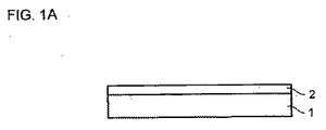
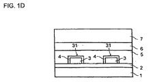
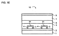
A)基板(1)上に第1の電極層(2)を準備するステップ、
B)前記第1の電極層(2)上に、金属を含有する構造化された導電層(3)を被着するステップ、
C)前記第1の電極層(2)に接していない前記導電層(3)の表面(31)上に、前記金属の酸化によって、前記導電層(3)の前記金属の酸化物を含有する絶縁層(4)を形成するステップ、
D)前記第1の電極層(2)および前記絶縁層(4)の上に、少なくとも1つの有機機能層(5)を被着するステップ、
E)前記少なくとも1つの有機機能層(5)上に第2の電極層(8)を被着するステップ、
を有することを特徴とする、有機発光素子の製造方法。 - 前記ステップC)において、酸素プラズマ処理、UVオゾン処理、反応性イオンエッチングおよび湿式化学的な処理から成るグループから選択された1つの方法または複数の方法の組み合わせによって酸化を行う、請求項1記載の方法。
- 前記ステップC)において、前記第1の電極層(2)を前記第1の電極層(2)の湿潤性および/または前記第1の電極層(2)の電気的な仕事関数に関して変性させる、請求項1または2記載の方法。
- 前記ステップB)において、前記導電層(3)の金属として卑金属を被着させ、該卑金属の酸化物を電気的に絶縁させる、請求項1から3までのいずれか1項記載の方法。
- 前記ステップC)において、前記絶縁層(4)を5ナノメートル以上かつ100ナノメートル以下の厚さでもって形成する、請求項1から4までのいずれか1項記載の方法。
- 前記ステップB)において、前記導電層(3)をスパッタリングまたは蒸着により被着させる、請求項1から5までのいずれか1項記載の方法。
- 前記ステップB)において、前記導電層(3)を帯状に構造化する、請求項1から6までのいずれか1項記載の方法。
- 前記導電層(3)の少なくとも1つの帯を前記電極層(2)の部分領域にわたり延在させる、請求項7記載の方法。
- 有機発光素子において、
基板(1)上の第1の電極層(2)と、
前記第1の電極層(2)上に配置されている、金属を含有する構造化された導電層(3)と、
前記第1の電極層(2)と接していない前記導電層(3)表面(31)上に配置されている、構造化された前記導電層(3)の前記金属の酸化物を含有する絶縁層(4)と
前記第1の電極層(2)および前記絶縁層(4)の上に配置されている少なくとも1つの有機機能層(5)と、
前記少なくとも1つの有機機能層(5)上に配置されている第2の電極層(8)とを有することを特徴とする、有機発光素子。 - 前記導電層(3)は卑金属を含有し、該卑金属の酸化物は電気的に絶縁されている、請求項9記載の有機発光素子。
- 前記絶縁層(4)は5ナノメートル以上かつ100ナノメートル以下の厚さを有する、請求項9または10記載の有機発光素子。
- 前記導電層(3)は帯状に構造化されている、請求項9から11までのいずれか1項記載の有機発光素子。
- 前記導電層(3)は、100ナノメートル以上かつ100マイクロメートル以下の幅の帯を少なくとも1つ有する、請求項12記載の有機発光素子。
- 前記絶縁層(4)は5ナノメートル以上かつ100ナノメートル以下の厚さを有する、請求項9から13までのいずれか1項記載の有機発光素子。
Applications Claiming Priority (3)
| Application Number | Priority Date | Filing Date | Title |
|---|---|---|---|
| DE102008045948.8 | 2008-09-04 | ||
| DE102008045948A DE102008045948A1 (de) | 2008-09-04 | 2008-09-04 | Verfahren zur Herstellung eines organischen strahlungsemittierenden Bauelements und organisches strahlungsemittierendes Bauelement |
| PCT/DE2009/001139 WO2010025696A2 (de) | 2008-09-04 | 2009-08-10 | Verfahren zur herstellung eines organischen strahlungsemittierenden bauelements und organisches strahlungsemittierendes bauelement |
Publications (2)
| Publication Number | Publication Date |
|---|---|
| JP2012502411A true JP2012502411A (ja) | 2012-01-26 |
| JP2012502411A5 JP2012502411A5 (ja) | 2012-08-02 |
Family
ID=41381647
Family Applications (1)
| Application Number | Title | Priority Date | Filing Date |
|---|---|---|---|
| JP2011525398A Pending JP2012502411A (ja) | 2008-09-04 | 2009-08-10 | 有機発光素子の製造方法および有機発光素子 |
Country Status (7)
| Country | Link |
|---|---|
| US (1) | US8927325B2 (ja) |
| EP (1) | EP2321863B1 (ja) |
| JP (1) | JP2012502411A (ja) |
| KR (1) | KR20110074518A (ja) |
| CN (1) | CN102144314B (ja) |
| DE (1) | DE102008045948A1 (ja) |
| WO (1) | WO2010025696A2 (ja) |
Cited By (2)
| Publication number | Priority date | Publication date | Assignee | Title |
|---|---|---|---|---|
| JP2012049112A (ja) * | 2010-07-26 | 2012-03-08 | Semiconductor Energy Lab Co Ltd | 発光装置、照明装置及び発光装置の作製方法 |
| JP2013077417A (ja) * | 2011-09-30 | 2013-04-25 | Mitsubishi Materials Corp | 有機エレクトロルミネッセンス素子およびその製造方法 |
Families Citing this family (18)
| Publication number | Priority date | Publication date | Assignee | Title |
|---|---|---|---|---|
| JP5829070B2 (ja) * | 2010-07-26 | 2015-12-09 | 株式会社半導体エネルギー研究所 | 発光装置、照明装置、及び発光装置の作製方法 |
| US20150047710A1 (en) * | 2012-03-26 | 2015-02-19 | Jawaharlal Nehru Centre For Advanced Scientific Research | Organic solar cell and methods thereof |
| US10326091B2 (en) | 2012-05-09 | 2019-06-18 | Lg Chem, Ltd. | Organic electrochemical device, and method for manufacturing same |
| DE102012109777A1 (de) * | 2012-10-15 | 2014-04-17 | Heliatek Gmbh | Verfahren zum Bedrucken optoelektronischer Bauelemente mit Stromsammelschienen |
| CN105393376B (zh) * | 2013-06-14 | 2017-11-17 | 株式会社Lg化学 | 有机太阳能电池及其制造方法 |
| DE102014110052B4 (de) * | 2014-07-17 | 2020-04-16 | Osram Oled Gmbh | Optoelektronisches Bauelement und Verfahren zum Herstellen eines optoelektronischen Bauelements |
| DE102014110978A1 (de) * | 2014-08-01 | 2016-02-04 | Osram Oled Gmbh | Organisches Licht emittierendes Bauelement |
| DE102014110969A1 (de) * | 2014-08-01 | 2016-02-04 | Osram Oled Gmbh | Organisches Bauteil sowie Verfahren zur Herstellung eines organischen Bauteils |
| DE102014112204A1 (de) * | 2014-08-26 | 2016-03-03 | Osram Oled Gmbh | Optoelektronische Vorrichtung |
| DE102014112618B4 (de) * | 2014-09-02 | 2023-09-07 | Pictiva Displays International Limited | Organisches Licht emittierendes Bauelement |
| DE102015101512A1 (de) * | 2015-02-03 | 2016-08-04 | Osram Oled Gmbh | Organisches elektronisches Bauelement |
| DE102015106630A1 (de) * | 2015-04-29 | 2016-11-03 | Osram Oled Gmbh | Organisches lichtemittierendes Bauelement und Verfahren zur Herstellung eines organischen lichtemittierenden Bauelements |
| DE102015110143B4 (de) * | 2015-06-24 | 2023-07-27 | Pictiva Displays International Limited | Organisches lichtemittierendes Bauelement und Verfahren zur Herstellung eines organischen lichtemittierenden Bauelements |
| DE102015212477A1 (de) * | 2015-07-03 | 2017-01-05 | Osram Oled Gmbh | Organisches lichtemittierendes Bauelement und Verfahren zur Herstellung eines organischen lichtemittierenden Bauelements |
| DE102015111564A1 (de) * | 2015-07-16 | 2017-01-19 | Osram Oled Gmbh | Organisches optoelektronisches Bauteil und Herstellungsverfahren hierfür |
| US20180016687A1 (en) * | 2016-07-13 | 2018-01-18 | Kabushiki Kaisha Toyota Chuo Kenkyusho | Method for producing nanoimprint transfer body |
| US20190390399A1 (en) * | 2018-06-26 | 2019-12-26 | Mycoworks, Inc. | Fungal composites comprising mycelium and an embedded material |
| EP3599648A1 (en) * | 2018-07-25 | 2020-01-29 | Nederlandse Organisatie voor toegepast- natuurwetenschappelijk onderzoek TNO | Photovoltaic device and method of manufacturing the same |
Citations (3)
| Publication number | Priority date | Publication date | Assignee | Title |
|---|---|---|---|---|
| JP2004134282A (ja) * | 2002-10-11 | 2004-04-30 | Matsushita Electric Ind Co Ltd | 照明装置及びそれを用いた画像読取装置 |
| JP2004349138A (ja) * | 2003-05-23 | 2004-12-09 | Toyota Industries Corp | 有機電界発光素子及びその製造方法 |
| WO2005106573A1 (ja) * | 2004-04-30 | 2005-11-10 | Fuji Photo Film Co., Ltd. | 液晶表示装置及びその製造方法 |
Family Cites Families (9)
| Publication number | Priority date | Publication date | Assignee | Title |
|---|---|---|---|---|
| JP3036436B2 (ja) | 1996-06-19 | 2000-04-24 | セイコーエプソン株式会社 | アクティブマトリックス型有機el表示体の製造方法 |
| JPH11339970A (ja) * | 1998-05-26 | 1999-12-10 | Tdk Corp | 有機el表示装置 |
| DE10324880B4 (de) * | 2003-05-30 | 2007-04-05 | Schott Ag | Verfahren zur Herstellung von OLEDs |
| US7122852B2 (en) * | 2004-05-12 | 2006-10-17 | Headway Technologies, Inc. | Structure/method to fabricate a high performance magnetic tunneling junction MRAM |
| JP4121514B2 (ja) | 2004-07-22 | 2008-07-23 | シャープ株式会社 | 有機発光素子、及び、それを備えた表示装置 |
| JPWO2007029756A1 (ja) | 2005-09-07 | 2009-03-19 | 旭硝子株式会社 | 補助配線付き基体およびその製造方法 |
| EP1887628A1 (en) * | 2006-07-20 | 2008-02-13 | Nederlandse Organisatie voor toegepast-natuurwetenschappelijk Onderzoek TNO | Electro-optical device |
| EP2089517A4 (en) * | 2006-10-23 | 2010-10-20 | Pacific Biosciences California | POLYMERASEENZYME AND REAGENTS FOR ADVANCED NUCKIC ACID SEQUENCING |
| JP5279254B2 (ja) * | 2007-12-18 | 2013-09-04 | キヤノン株式会社 | 有機発光素子及び表示装置 |
-
2008
- 2008-09-04 DE DE102008045948A patent/DE102008045948A1/de not_active Withdrawn
-
2009
- 2009-08-10 JP JP2011525398A patent/JP2012502411A/ja active Pending
- 2009-08-10 EP EP09776086.2A patent/EP2321863B1/de active Active
- 2009-08-10 WO PCT/DE2009/001139 patent/WO2010025696A2/de active Application Filing
- 2009-08-10 CN CN200980134746.9A patent/CN102144314B/zh active Active
- 2009-08-10 US US13/062,449 patent/US8927325B2/en active Active
- 2009-08-10 KR KR1020117007684A patent/KR20110074518A/ko not_active Application Discontinuation
Patent Citations (3)
| Publication number | Priority date | Publication date | Assignee | Title |
|---|---|---|---|---|
| JP2004134282A (ja) * | 2002-10-11 | 2004-04-30 | Matsushita Electric Ind Co Ltd | 照明装置及びそれを用いた画像読取装置 |
| JP2004349138A (ja) * | 2003-05-23 | 2004-12-09 | Toyota Industries Corp | 有機電界発光素子及びその製造方法 |
| WO2005106573A1 (ja) * | 2004-04-30 | 2005-11-10 | Fuji Photo Film Co., Ltd. | 液晶表示装置及びその製造方法 |
Cited By (4)
| Publication number | Priority date | Publication date | Assignee | Title |
|---|---|---|---|---|
| JP2012049112A (ja) * | 2010-07-26 | 2012-03-08 | Semiconductor Energy Lab Co Ltd | 発光装置、照明装置及び発光装置の作製方法 |
| JP2016035941A (ja) * | 2010-07-26 | 2016-03-17 | 株式会社半導体エネルギー研究所 | 発光装置 |
| US9728737B2 (en) | 2010-07-26 | 2017-08-08 | Semiconductor Energy Laboratory Co., Ltd. | Light-emitting device, lighting device, and manufacturing method of light-emitting device |
| JP2013077417A (ja) * | 2011-09-30 | 2013-04-25 | Mitsubishi Materials Corp | 有機エレクトロルミネッセンス素子およびその製造方法 |
Also Published As
| Publication number | Publication date |
|---|---|
| CN102144314A (zh) | 2011-08-03 |
| DE102008045948A1 (de) | 2010-03-11 |
| EP2321863A2 (de) | 2011-05-18 |
| WO2010025696A2 (de) | 2010-03-11 |
| EP2321863B1 (de) | 2018-10-10 |
| US20110266588A1 (en) | 2011-11-03 |
| US8927325B2 (en) | 2015-01-06 |
| KR20110074518A (ko) | 2011-06-30 |
| CN102144314B (zh) | 2015-04-22 |
| WO2010025696A3 (de) | 2010-07-29 |
Similar Documents
| Publication | Publication Date | Title |
|---|---|---|
| JP2012502411A (ja) | 有機発光素子の製造方法および有機発光素子 | |
| JP5612691B2 (ja) | 有機el素子およびその製造方法 | |
| JP5612693B2 (ja) | 有機el素子およびその製造方法 | |
| KR101182435B1 (ko) | 전도성 고분자 패턴막 및 이를 패터닝 하는 방법 그리고 이를 이용하는 유기전계 발광소자 및 그 제조방법 | |
| US10290687B2 (en) | Lighting apparatus using organic light emitting diode and method of fabricating the same | |
| JP5612692B2 (ja) | 有機el素子およびその製造方法 | |
| KR20140128308A (ko) | 유기 전자 소자 및 유기 전자 소자의 제조 방법 | |
| US20110198657A1 (en) | Organic Light-Emitting Diode, Contact Arrangement and Method for Producing an Organic Light-Emitting Diode | |
| JPWO2010038356A1 (ja) | 有機elデバイスおよびその製造方法 | |
| JP2013514612A (ja) | 均一な温度分布を有する有機発光装置 | |
| US8969860B2 (en) | Organic electroluminescent lighting device and method for manufacturing the lighting device | |
| KR20030017748A (ko) | 유기물 전계 효과 트랜지스터와 유기물 발광 다이오드가일체화된 유기물 전기 발광 소자 및 그 제조 방법 | |
| JP2013516735A (ja) | 有機発光ダイオード装置のマスクレス製造の方法 | |
| JP2013514621A (ja) | 直列に接続されたoledデバイスを生成するための方法 | |
| US20180198087A1 (en) | Organic light-emitting component and method for producing an organic light-emitting component | |
| KR100942498B1 (ko) | 유기발광장치의 제조방법 | |
| KR101486844B1 (ko) | 복사 방출 장치 및 복사 방출 장치의 제조 방법 | |
| JP6751747B2 (ja) | 照明装置用oledパネル及びその製造方法 | |
| US20210399169A1 (en) | Optoelectronic semiconductor chip and method for producing an optoelectronic semiconductor chip | |
| KR102482208B1 (ko) | 표시품질이 향상된 유기발광소자 | |
| KR20060084210A (ko) | 유기 el 소자 | |
| WO2018235594A1 (ja) | 透明電極の製造方法及び電子デバイスの製造方法 | |
| KR20130033100A (ko) | 유기전계 발광소자 | |
| KR20110103050A (ko) | 유기전계 발광소자의 제조 방법 |
Legal Events
| Date | Code | Title | Description |
|---|---|---|---|
| A521 | Request for written amendment filed |
Free format text: JAPANESE INTERMEDIATE CODE: A523 Effective date: 20120614 |
|
| A621 | Written request for application examination |
Free format text: JAPANESE INTERMEDIATE CODE: A621 Effective date: 20120614 |
|
| A131 | Notification of reasons for refusal |
Free format text: JAPANESE INTERMEDIATE CODE: A131 Effective date: 20130313 |
|
| A977 | Report on retrieval |
Free format text: JAPANESE INTERMEDIATE CODE: A971007 Effective date: 20130313 |
|
| A521 | Request for written amendment filed |
Free format text: JAPANESE INTERMEDIATE CODE: A523 Effective date: 20130605 |
|
| A02 | Decision of refusal |
Free format text: JAPANESE INTERMEDIATE CODE: A02 Effective date: 20130701 |