JP2011523902A - ナノワイヤアレイを製造するためのプロセス - Google Patents
ナノワイヤアレイを製造するためのプロセス Download PDFInfo
- Publication number
- JP2011523902A JP2011523902A JP2011505144A JP2011505144A JP2011523902A JP 2011523902 A JP2011523902 A JP 2011523902A JP 2011505144 A JP2011505144 A JP 2011505144A JP 2011505144 A JP2011505144 A JP 2011505144A JP 2011523902 A JP2011523902 A JP 2011523902A
- Authority
- JP
- Japan
- Prior art keywords
- silicon
- array
- nanowires
- metal
- less
- Prior art date
- Legal status (The legal status is an assumption and is not a legal conclusion. Google has not performed a legal analysis and makes no representation as to the accuracy of the status listed.)
- Pending
Links
Images


Classifications
-
- B—PERFORMING OPERATIONS; TRANSPORTING
- B01—PHYSICAL OR CHEMICAL PROCESSES OR APPARATUS IN GENERAL
- B01J—CHEMICAL OR PHYSICAL PROCESSES, e.g. CATALYSIS OR COLLOID CHEMISTRY; THEIR RELEVANT APPARATUS
- B01J20/00—Solid sorbent compositions or filter aid compositions; Sorbents for chromatography; Processes for preparing, regenerating or reactivating thereof
- B01J20/02—Solid sorbent compositions or filter aid compositions; Sorbents for chromatography; Processes for preparing, regenerating or reactivating thereof comprising inorganic material
- B01J20/10—Solid sorbent compositions or filter aid compositions; Sorbents for chromatography; Processes for preparing, regenerating or reactivating thereof comprising inorganic material comprising silica or silicate
-
- H—ELECTRICITY
- H10—SEMICONDUCTOR DEVICES; ELECTRIC SOLID-STATE DEVICES NOT OTHERWISE PROVIDED FOR
- H10D—INORGANIC ELECTRIC SEMICONDUCTOR DEVICES
- H10D62/00—Semiconductor bodies, or regions thereof, of devices having potential barriers
- H10D62/10—Shapes, relative sizes or dispositions of the regions of the semiconductor bodies; Shapes of the semiconductor bodies
- H10D62/117—Shapes of semiconductor bodies
- H10D62/118—Nanostructure semiconductor bodies
- H10D62/119—Nanowire, nanosheet or nanotube semiconductor bodies
-
- B—PERFORMING OPERATIONS; TRANSPORTING
- B01—PHYSICAL OR CHEMICAL PROCESSES OR APPARATUS IN GENERAL
- B01J—CHEMICAL OR PHYSICAL PROCESSES, e.g. CATALYSIS OR COLLOID CHEMISTRY; THEIR RELEVANT APPARATUS
- B01J20/00—Solid sorbent compositions or filter aid compositions; Sorbents for chromatography; Processes for preparing, regenerating or reactivating thereof
- B01J20/28—Solid sorbent compositions or filter aid compositions; Sorbents for chromatography; Processes for preparing, regenerating or reactivating thereof characterised by their form or physical properties
- B01J20/28002—Solid sorbent compositions or filter aid compositions; Sorbents for chromatography; Processes for preparing, regenerating or reactivating thereof characterised by their form or physical properties characterised by their physical properties
- B01J20/28004—Sorbent size or size distribution, e.g. particle size
- B01J20/28007—Sorbent size or size distribution, e.g. particle size with size in the range 1-100 nanometers, e.g. nanosized particles, nanofibers, nanotubes, nanowires or the like
-
- B—PERFORMING OPERATIONS; TRANSPORTING
- B82—NANOTECHNOLOGY
- B82Y—SPECIFIC USES OR APPLICATIONS OF NANOSTRUCTURES; MEASUREMENT OR ANALYSIS OF NANOSTRUCTURES; MANUFACTURE OR TREATMENT OF NANOSTRUCTURES
- B82Y20/00—Nanooptics, e.g. quantum optics or photonic crystals
-
- B—PERFORMING OPERATIONS; TRANSPORTING
- B82—NANOTECHNOLOGY
- B82Y—SPECIFIC USES OR APPLICATIONS OF NANOSTRUCTURES; MEASUREMENT OR ANALYSIS OF NANOSTRUCTURES; MANUFACTURE OR TREATMENT OF NANOSTRUCTURES
- B82Y30/00—Nanotechnology for materials or surface science, e.g. nanocomposites
-
- C—CHEMISTRY; METALLURGY
- C23—COATING METALLIC MATERIAL; COATING MATERIAL WITH METALLIC MATERIAL; CHEMICAL SURFACE TREATMENT; DIFFUSION TREATMENT OF METALLIC MATERIAL; COATING BY VACUUM EVAPORATION, BY SPUTTERING, BY ION IMPLANTATION OR BY CHEMICAL VAPOUR DEPOSITION, IN GENERAL; INHIBITING CORROSION OF METALLIC MATERIAL OR INCRUSTATION IN GENERAL
- C23C—COATING METALLIC MATERIAL; COATING MATERIAL WITH METALLIC MATERIAL; SURFACE TREATMENT OF METALLIC MATERIAL BY DIFFUSION INTO THE SURFACE, BY CHEMICAL CONVERSION OR SUBSTITUTION; COATING BY VACUUM EVAPORATION, BY SPUTTERING, BY ION IMPLANTATION OR BY CHEMICAL VAPOUR DEPOSITION, IN GENERAL
- C23C14/00—Coating by vacuum evaporation, by sputtering or by ion implantation of the coating forming material
- C23C14/22—Coating by vacuum evaporation, by sputtering or by ion implantation of the coating forming material characterised by the process of coating
- C23C14/34—Sputtering
-
- H—ELECTRICITY
- H01—ELECTRIC ELEMENTS
- H01M—PROCESSES OR MEANS, e.g. BATTERIES, FOR THE DIRECT CONVERSION OF CHEMICAL ENERGY INTO ELECTRICAL ENERGY
- H01M4/00—Electrodes
- H01M4/02—Electrodes composed of, or comprising, active material
- H01M4/04—Processes of manufacture in general
- H01M4/049—Manufacturing of an active layer by chemical means
- H01M4/0492—Chemical attack of the support material
-
- H—ELECTRICITY
- H01—ELECTRIC ELEMENTS
- H01M—PROCESSES OR MEANS, e.g. BATTERIES, FOR THE DIRECT CONVERSION OF CHEMICAL ENERGY INTO ELECTRICAL ENERGY
- H01M4/00—Electrodes
- H01M4/02—Electrodes composed of, or comprising, active material
- H01M4/13—Electrodes for accumulators with non-aqueous electrolyte, e.g. for lithium-accumulators; Processes of manufacture thereof
- H01M4/134—Electrodes based on metals, Si or alloys
-
- H—ELECTRICITY
- H01—ELECTRIC ELEMENTS
- H01M—PROCESSES OR MEANS, e.g. BATTERIES, FOR THE DIRECT CONVERSION OF CHEMICAL ENERGY INTO ELECTRICAL ENERGY
- H01M4/00—Electrodes
- H01M4/02—Electrodes composed of, or comprising, active material
- H01M4/36—Selection of substances as active materials, active masses, active liquids
- H01M4/362—Composites
- H01M4/366—Composites as layered products
-
- H—ELECTRICITY
- H01—ELECTRIC ELEMENTS
- H01M—PROCESSES OR MEANS, e.g. BATTERIES, FOR THE DIRECT CONVERSION OF CHEMICAL ENERGY INTO ELECTRICAL ENERGY
- H01M4/00—Electrodes
- H01M4/02—Electrodes composed of, or comprising, active material
- H01M4/36—Selection of substances as active materials, active masses, active liquids
- H01M4/38—Selection of substances as active materials, active masses, active liquids of elements or alloys
- H01M4/386—Silicon or alloys based on silicon
-
- H—ELECTRICITY
- H10—SEMICONDUCTOR DEVICES; ELECTRIC SOLID-STATE DEVICES NOT OTHERWISE PROVIDED FOR
- H10D—INORGANIC ELECTRIC SEMICONDUCTOR DEVICES
- H10D62/00—Semiconductor bodies, or regions thereof, of devices having potential barriers
- H10D62/10—Shapes, relative sizes or dispositions of the regions of the semiconductor bodies; Shapes of the semiconductor bodies
- H10D62/117—Shapes of semiconductor bodies
- H10D62/118—Nanostructure semiconductor bodies
- H10D62/119—Nanowire, nanosheet or nanotube semiconductor bodies
- H10D62/122—Nanowire, nanosheet or nanotube semiconductor bodies oriented at angles to substrates, e.g. perpendicular to substrates
-
- H—ELECTRICITY
- H10—SEMICONDUCTOR DEVICES; ELECTRIC SOLID-STATE DEVICES NOT OTHERWISE PROVIDED FOR
- H10D—INORGANIC ELECTRIC SEMICONDUCTOR DEVICES
- H10D62/00—Semiconductor bodies, or regions thereof, of devices having potential barriers
- H10D62/40—Crystalline structures
-
- H—ELECTRICITY
- H10—SEMICONDUCTOR DEVICES; ELECTRIC SOLID-STATE DEVICES NOT OTHERWISE PROVIDED FOR
- H10D—INORGANIC ELECTRIC SEMICONDUCTOR DEVICES
- H10D62/00—Semiconductor bodies, or regions thereof, of devices having potential barriers
- H10D62/80—Semiconductor bodies, or regions thereof, of devices having potential barriers characterised by the materials
- H10D62/83—Semiconductor bodies, or regions thereof, of devices having potential barriers characterised by the materials being Group IV materials, e.g. B-doped Si or undoped Ge
-
- H—ELECTRICITY
- H10—SEMICONDUCTOR DEVICES; ELECTRIC SOLID-STATE DEVICES NOT OTHERWISE PROVIDED FOR
- H10F—INORGANIC SEMICONDUCTOR DEVICES SENSITIVE TO INFRARED RADIATION, LIGHT, ELECTROMAGNETIC RADIATION OF SHORTER WAVELENGTH OR CORPUSCULAR RADIATION
- H10F77/00—Constructional details of devices covered by this subclass
- H10F77/10—Semiconductor bodies
- H10F77/12—Active materials
- H10F77/122—Active materials comprising only Group IV materials
-
- H—ELECTRICITY
- H10—SEMICONDUCTOR DEVICES; ELECTRIC SOLID-STATE DEVICES NOT OTHERWISE PROVIDED FOR
- H10F—INORGANIC SEMICONDUCTOR DEVICES SENSITIVE TO INFRARED RADIATION, LIGHT, ELECTROMAGNETIC RADIATION OF SHORTER WAVELENGTH OR CORPUSCULAR RADIATION
- H10F77/00—Constructional details of devices covered by this subclass
- H10F77/10—Semiconductor bodies
- H10F77/14—Shape of semiconductor bodies; Shapes, relative sizes or dispositions of semiconductor regions within semiconductor bodies
-
- H—ELECTRICITY
- H10—SEMICONDUCTOR DEVICES; ELECTRIC SOLID-STATE DEVICES NOT OTHERWISE PROVIDED FOR
- H10F—INORGANIC SEMICONDUCTOR DEVICES SENSITIVE TO INFRARED RADIATION, LIGHT, ELECTROMAGNETIC RADIATION OF SHORTER WAVELENGTH OR CORPUSCULAR RADIATION
- H10F77/00—Constructional details of devices covered by this subclass
- H10F77/70—Surface textures, e.g. pyramid structures
-
- H—ELECTRICITY
- H10—SEMICONDUCTOR DEVICES; ELECTRIC SOLID-STATE DEVICES NOT OTHERWISE PROVIDED FOR
- H10F—INORGANIC SEMICONDUCTOR DEVICES SENSITIVE TO INFRARED RADIATION, LIGHT, ELECTROMAGNETIC RADIATION OF SHORTER WAVELENGTH OR CORPUSCULAR RADIATION
- H10F77/00—Constructional details of devices covered by this subclass
- H10F77/70—Surface textures, e.g. pyramid structures
- H10F77/703—Surface textures, e.g. pyramid structures of the semiconductor bodies, e.g. textured active layers
-
- H—ELECTRICITY
- H10—SEMICONDUCTOR DEVICES; ELECTRIC SOLID-STATE DEVICES NOT OTHERWISE PROVIDED FOR
- H10P—GENERIC PROCESSES OR APPARATUS FOR THE MANUFACTURE OR TREATMENT OF DEVICES COVERED BY CLASS H10
- H10P14/00—Formation of materials, e.g. in the shape of layers or pillars
- H10P14/20—Formation of materials, e.g. in the shape of layers or pillars of semiconductor materials
- H10P14/32—Formation of materials, e.g. in the shape of layers or pillars of semiconductor materials characterised by intermediate layers between substrates and deposited layers
- H10P14/3202—Materials thereof
- H10P14/3238—Materials thereof being insulating materials
-
- H—ELECTRICITY
- H10—SEMICONDUCTOR DEVICES; ELECTRIC SOLID-STATE DEVICES NOT OTHERWISE PROVIDED FOR
- H10P—GENERIC PROCESSES OR APPARATUS FOR THE MANUFACTURE OR TREATMENT OF DEVICES COVERED BY CLASS H10
- H10P14/00—Formation of materials, e.g. in the shape of layers or pillars
- H10P14/20—Formation of materials, e.g. in the shape of layers or pillars of semiconductor materials
- H10P14/32—Formation of materials, e.g. in the shape of layers or pillars of semiconductor materials characterised by intermediate layers between substrates and deposited layers
- H10P14/3242—Structure
- H10P14/3256—Microstructure
-
- H—ELECTRICITY
- H10—SEMICONDUCTOR DEVICES; ELECTRIC SOLID-STATE DEVICES NOT OTHERWISE PROVIDED FOR
- H10P—GENERIC PROCESSES OR APPARATUS FOR THE MANUFACTURE OR TREATMENT OF DEVICES COVERED BY CLASS H10
- H10P14/00—Formation of materials, e.g. in the shape of layers or pillars
- H10P14/20—Formation of materials, e.g. in the shape of layers or pillars of semiconductor materials
- H10P14/34—Deposited materials, e.g. layers
- H10P14/3402—Deposited materials, e.g. layers characterised by the chemical composition
- H10P14/3404—Deposited materials, e.g. layers characterised by the chemical composition being Group IVA materials
- H10P14/3411—Silicon, silicon germanium or germanium
-
- H—ELECTRICITY
- H10—SEMICONDUCTOR DEVICES; ELECTRIC SOLID-STATE DEVICES NOT OTHERWISE PROVIDED FOR
- H10P—GENERIC PROCESSES OR APPARATUS FOR THE MANUFACTURE OR TREATMENT OF DEVICES COVERED BY CLASS H10
- H10P14/00—Formation of materials, e.g. in the shape of layers or pillars
- H10P14/20—Formation of materials, e.g. in the shape of layers or pillars of semiconductor materials
- H10P14/34—Deposited materials, e.g. layers
- H10P14/3451—Structure
- H10P14/3452—Microstructure
- H10P14/3462—Nanowires
-
- H—ELECTRICITY
- H10—SEMICONDUCTOR DEVICES; ELECTRIC SOLID-STATE DEVICES NOT OTHERWISE PROVIDED FOR
- H10P—GENERIC PROCESSES OR APPARATUS FOR THE MANUFACTURE OR TREATMENT OF DEVICES COVERED BY CLASS H10
- H10P14/00—Formation of materials, e.g. in the shape of layers or pillars
- H10P14/40—Formation of materials, e.g. in the shape of layers or pillars of conductive or resistive materials
- H10P14/418—Formation of materials, e.g. in the shape of layers or pillars of conductive or resistive materials the conductive layers comprising transition metals
-
- H—ELECTRICITY
- H10—SEMICONDUCTOR DEVICES; ELECTRIC SOLID-STATE DEVICES NOT OTHERWISE PROVIDED FOR
- H10P—GENERIC PROCESSES OR APPARATUS FOR THE MANUFACTURE OR TREATMENT OF DEVICES COVERED BY CLASS H10
- H10P14/00—Formation of materials, e.g. in the shape of layers or pillars
- H10P14/40—Formation of materials, e.g. in the shape of layers or pillars of conductive or resistive materials
- H10P14/42—Formation of materials, e.g. in the shape of layers or pillars of conductive or resistive materials using a gas or vapour
- H10P14/44—Physical vapour deposition [PVD]
-
- H—ELECTRICITY
- H10—SEMICONDUCTOR DEVICES; ELECTRIC SOLID-STATE DEVICES NOT OTHERWISE PROVIDED FOR
- H10P—GENERIC PROCESSES OR APPARATUS FOR THE MANUFACTURE OR TREATMENT OF DEVICES COVERED BY CLASS H10
- H10P14/00—Formation of materials, e.g. in the shape of layers or pillars
- H10P14/60—Formation of materials, e.g. in the shape of layers or pillars of insulating materials
- H10P14/63—Formation of materials, e.g. in the shape of layers or pillars of insulating materials characterised by the formation processes
- H10P14/6302—Non-deposition formation processes
- H10P14/6304—Formation by oxidation, e.g. oxidation of the substrate
- H10P14/6314—Formation by oxidation, e.g. oxidation of the substrate of a metallic layer
-
- H—ELECTRICITY
- H10—SEMICONDUCTOR DEVICES; ELECTRIC SOLID-STATE DEVICES NOT OTHERWISE PROVIDED FOR
- H10P—GENERIC PROCESSES OR APPARATUS FOR THE MANUFACTURE OR TREATMENT OF DEVICES COVERED BY CLASS H10
- H10P14/00—Formation of materials, e.g. in the shape of layers or pillars
- H10P14/60—Formation of materials, e.g. in the shape of layers or pillars of insulating materials
- H10P14/63—Formation of materials, e.g. in the shape of layers or pillars of insulating materials characterised by the formation processes
- H10P14/6326—Deposition processes
- H10P14/6342—Liquid deposition, e.g. spin-coating, sol-gel techniques or spray coating
-
- H—ELECTRICITY
- H10—SEMICONDUCTOR DEVICES; ELECTRIC SOLID-STATE DEVICES NOT OTHERWISE PROVIDED FOR
- H10P—GENERIC PROCESSES OR APPARATUS FOR THE MANUFACTURE OR TREATMENT OF DEVICES COVERED BY CLASS H10
- H10P14/00—Formation of materials, e.g. in the shape of layers or pillars
- H10P14/60—Formation of materials, e.g. in the shape of layers or pillars of insulating materials
- H10P14/65—Formation of materials, e.g. in the shape of layers or pillars of insulating materials characterised by treatments performed before or after the formation of the materials
- H10P14/6502—Formation of materials, e.g. in the shape of layers or pillars of insulating materials characterised by treatments performed before or after the formation of the materials of treatments performed before formation of the materials
- H10P14/6508—Formation of materials, e.g. in the shape of layers or pillars of insulating materials characterised by treatments performed before or after the formation of the materials of treatments performed before formation of the materials by exposure to a liquid
-
- H—ELECTRICITY
- H10—SEMICONDUCTOR DEVICES; ELECTRIC SOLID-STATE DEVICES NOT OTHERWISE PROVIDED FOR
- H10P—GENERIC PROCESSES OR APPARATUS FOR THE MANUFACTURE OR TREATMENT OF DEVICES COVERED BY CLASS H10
- H10P14/00—Formation of materials, e.g. in the shape of layers or pillars
- H10P14/60—Formation of materials, e.g. in the shape of layers or pillars of insulating materials
- H10P14/65—Formation of materials, e.g. in the shape of layers or pillars of insulating materials characterised by treatments performed before or after the formation of the materials
- H10P14/6516—Formation of materials, e.g. in the shape of layers or pillars of insulating materials characterised by treatments performed before or after the formation of the materials of treatments performed after formation of the materials
- H10P14/6529—Formation of materials, e.g. in the shape of layers or pillars of insulating materials characterised by treatments performed before or after the formation of the materials of treatments performed after formation of the materials by exposure to a gas or vapour
- H10P14/6532—Formation of materials, e.g. in the shape of layers or pillars of insulating materials characterised by treatments performed before or after the formation of the materials of treatments performed after formation of the materials by exposure to a gas or vapour by exposure to a plasma
-
- H—ELECTRICITY
- H10—SEMICONDUCTOR DEVICES; ELECTRIC SOLID-STATE DEVICES NOT OTHERWISE PROVIDED FOR
- H10P—GENERIC PROCESSES OR APPARATUS FOR THE MANUFACTURE OR TREATMENT OF DEVICES COVERED BY CLASS H10
- H10P14/00—Formation of materials, e.g. in the shape of layers or pillars
- H10P14/60—Formation of materials, e.g. in the shape of layers or pillars of insulating materials
- H10P14/68—Organic materials, e.g. photoresists
- H10P14/683—Organic materials, e.g. photoresists carbon-based polymeric organic materials, e.g. polyimides, poly cyclobutene or PVC
-
- H—ELECTRICITY
- H10—SEMICONDUCTOR DEVICES; ELECTRIC SOLID-STATE DEVICES NOT OTHERWISE PROVIDED FOR
- H10P—GENERIC PROCESSES OR APPARATUS FOR THE MANUFACTURE OR TREATMENT OF DEVICES COVERED BY CLASS H10
- H10P14/00—Formation of materials, e.g. in the shape of layers or pillars
- H10P14/60—Formation of materials, e.g. in the shape of layers or pillars of insulating materials
- H10P14/69—Inorganic materials
- H10P14/692—Inorganic materials composed of oxides, glassy oxides or oxide-based glasses
- H10P14/6921—Inorganic materials composed of oxides, glassy oxides or oxide-based glasses containing silicon
- H10P14/69215—Inorganic materials composed of oxides, glassy oxides or oxide-based glasses containing silicon the material being a silicon oxide, e.g. SiO2
-
- H—ELECTRICITY
- H10—SEMICONDUCTOR DEVICES; ELECTRIC SOLID-STATE DEVICES NOT OTHERWISE PROVIDED FOR
- H10P—GENERIC PROCESSES OR APPARATUS FOR THE MANUFACTURE OR TREATMENT OF DEVICES COVERED BY CLASS H10
- H10P14/00—Formation of materials, e.g. in the shape of layers or pillars
- H10P14/60—Formation of materials, e.g. in the shape of layers or pillars of insulating materials
- H10P14/69—Inorganic materials
- H10P14/692—Inorganic materials composed of oxides, glassy oxides or oxide-based glasses
- H10P14/6938—Inorganic materials composed of oxides, glassy oxides or oxide-based glasses the material containing at least one metal element, e.g. metal oxides, metal oxynitrides or metal oxycarbides
- H10P14/6939—Inorganic materials composed of oxides, glassy oxides or oxide-based glasses the material containing at least one metal element, e.g. metal oxides, metal oxynitrides or metal oxycarbides characterised by the metal
-
- H—ELECTRICITY
- H10—SEMICONDUCTOR DEVICES; ELECTRIC SOLID-STATE DEVICES NOT OTHERWISE PROVIDED FOR
- H10P—GENERIC PROCESSES OR APPARATUS FOR THE MANUFACTURE OR TREATMENT OF DEVICES COVERED BY CLASS H10
- H10P50/00—Etching of wafers, substrates or parts of devices
- H10P50/60—Wet etching
- H10P50/64—Wet etching of semiconductor materials
- H10P50/642—Chemical etching
-
- H—ELECTRICITY
- H10—SEMICONDUCTOR DEVICES; ELECTRIC SOLID-STATE DEVICES NOT OTHERWISE PROVIDED FOR
- H10P—GENERIC PROCESSES OR APPARATUS FOR THE MANUFACTURE OR TREATMENT OF DEVICES COVERED BY CLASS H10
- H10P50/00—Etching of wafers, substrates or parts of devices
- H10P50/60—Wet etching
- H10P50/66—Wet etching of conductive or resistive materials
- H10P50/663—Wet etching of conductive or resistive materials by chemical means only
- H10P50/667—Wet etching of conductive or resistive materials by chemical means only by liquid etching only
-
- H—ELECTRICITY
- H10—SEMICONDUCTOR DEVICES; ELECTRIC SOLID-STATE DEVICES NOT OTHERWISE PROVIDED FOR
- H10P—GENERIC PROCESSES OR APPARATUS FOR THE MANUFACTURE OR TREATMENT OF DEVICES COVERED BY CLASS H10
- H10P50/00—Etching of wafers, substrates or parts of devices
- H10P50/69—Etching of wafers, substrates or parts of devices using masks for semiconductor materials
- H10P50/691—Etching of wafers, substrates or parts of devices using masks for semiconductor materials for Group V materials or Group III-V materials
- H10P50/693—Etching of wafers, substrates or parts of devices using masks for semiconductor materials for Group V materials or Group III-V materials characterised by their size, orientation, disposition, behaviour or shape, in horizontal or vertical plane
- H10P50/695—Etching of wafers, substrates or parts of devices using masks for semiconductor materials for Group V materials or Group III-V materials characterised by their size, orientation, disposition, behaviour or shape, in horizontal or vertical plane characterised by the process involved to create the mask, e.g. lift-off masks or sidewalls or to modify the mask
-
- H—ELECTRICITY
- H01—ELECTRIC ELEMENTS
- H01M—PROCESSES OR MEANS, e.g. BATTERIES, FOR THE DIRECT CONVERSION OF CHEMICAL ENERGY INTO ELECTRICAL ENERGY
- H01M10/00—Secondary cells; Manufacture thereof
- H01M10/05—Accumulators with non-aqueous electrolyte
- H01M10/052—Li-accumulators
- H01M10/0525—Rocking-chair batteries, i.e. batteries with lithium insertion or intercalation in both electrodes; Lithium-ion batteries
-
- H—ELECTRICITY
- H01—ELECTRIC ELEMENTS
- H01M—PROCESSES OR MEANS, e.g. BATTERIES, FOR THE DIRECT CONVERSION OF CHEMICAL ENERGY INTO ELECTRICAL ENERGY
- H01M4/00—Electrodes
- H01M4/02—Electrodes composed of, or comprising, active material
- H01M2004/026—Electrodes composed of, or comprising, active material characterised by the polarity
- H01M2004/027—Negative electrodes
-
- H—ELECTRICITY
- H01—ELECTRIC ELEMENTS
- H01M—PROCESSES OR MEANS, e.g. BATTERIES, FOR THE DIRECT CONVERSION OF CHEMICAL ENERGY INTO ELECTRICAL ENERGY
- H01M4/00—Electrodes
- H01M4/02—Electrodes composed of, or comprising, active material
- H01M4/13—Electrodes for accumulators with non-aqueous electrolyte, e.g. for lithium-accumulators; Processes of manufacture thereof
- H01M4/139—Processes of manufacture
- H01M4/1395—Processes of manufacture of electrodes based on metals, Si or alloys
-
- H—ELECTRICITY
- H01—ELECTRIC ELEMENTS
- H01M—PROCESSES OR MEANS, e.g. BATTERIES, FOR THE DIRECT CONVERSION OF CHEMICAL ENERGY INTO ELECTRICAL ENERGY
- H01M4/00—Electrodes
- H01M4/02—Electrodes composed of, or comprising, active material
- H01M4/64—Carriers or collectors
- H01M4/66—Selection of materials
- H01M4/661—Metal or alloys, e.g. alloy coatings
-
- Y—GENERAL TAGGING OF NEW TECHNOLOGICAL DEVELOPMENTS; GENERAL TAGGING OF CROSS-SECTIONAL TECHNOLOGIES SPANNING OVER SEVERAL SECTIONS OF THE IPC; TECHNICAL SUBJECTS COVERED BY FORMER USPC CROSS-REFERENCE ART COLLECTIONS [XRACs] AND DIGESTS
- Y02—TECHNOLOGIES OR APPLICATIONS FOR MITIGATION OR ADAPTATION AGAINST CLIMATE CHANGE
- Y02E—REDUCTION OF GREENHOUSE GAS [GHG] EMISSIONS, RELATED TO ENERGY GENERATION, TRANSMISSION OR DISTRIBUTION
- Y02E10/00—Energy generation through renewable energy sources
- Y02E10/50—Photovoltaic [PV] energy
-
- Y—GENERAL TAGGING OF NEW TECHNOLOGICAL DEVELOPMENTS; GENERAL TAGGING OF CROSS-SECTIONAL TECHNOLOGIES SPANNING OVER SEVERAL SECTIONS OF THE IPC; TECHNICAL SUBJECTS COVERED BY FORMER USPC CROSS-REFERENCE ART COLLECTIONS [XRACs] AND DIGESTS
- Y10—TECHNICAL SUBJECTS COVERED BY FORMER USPC
- Y10S—TECHNICAL SUBJECTS COVERED BY FORMER USPC CROSS-REFERENCE ART COLLECTIONS [XRACs] AND DIGESTS
- Y10S977/00—Nanotechnology
- Y10S977/70—Nanostructure
- Y10S977/762—Nanowire or quantum wire, i.e. axially elongated structure having two dimensions of 100 nm or less
Landscapes
- Chemical & Material Sciences (AREA)
- Engineering & Computer Science (AREA)
- Chemical Kinetics & Catalysis (AREA)
- Nanotechnology (AREA)
- General Chemical & Material Sciences (AREA)
- Materials Engineering (AREA)
- Electrochemistry (AREA)
- Crystallography & Structural Chemistry (AREA)
- Composite Materials (AREA)
- Organic Chemistry (AREA)
- Physics & Mathematics (AREA)
- Analytical Chemistry (AREA)
- Life Sciences & Earth Sciences (AREA)
- Inorganic Chemistry (AREA)
- Condensed Matter Physics & Semiconductors (AREA)
- General Physics & Mathematics (AREA)
- Biophysics (AREA)
- Optics & Photonics (AREA)
- Metallurgy (AREA)
- Mechanical Engineering (AREA)
- Manufacturing & Machinery (AREA)
- Silicon Compounds (AREA)
- Plasma & Fusion (AREA)
- Weting (AREA)
- Battery Electrode And Active Subsutance (AREA)
Abstract
ナノワイヤアレイを形成するために、シリコン含有基板をエッチングするためのプロセスが提供される。このプロセスにおいて、ある者は、金属が、エッチングが所望される場所に存在してシリコンに触れ、それ以外の場所において、シリコンに触れることがブロックされ、または存在しないような態様で、基板上にナノ粒子および金属膜を堆積させる。ある者は、金属化された基板を、HFと酸化因子とを含むエッチング水溶液の中へ沈める。このような態様で、制御された直径および長さを有するナノワイヤのアレイが生産される。
Description
(関連出願の相互参照)
本出願は、2008年4月14日出願の米国仮特許出願第61/044,573号および2008年12月29日出願の米国仮特許出願第61/141,082号の優先権を主張する。当該仮特許出願は本明細書において参照により援用される。
本出願は、2008年4月14日出願の米国仮特許出願第61/044,573号および2008年12月29日出願の米国仮特許出願第61/141,082号の優先権を主張する。当該仮特許出願は本明細書において参照により援用される。
(技術分野)
本出願は、ナノテクノロジの分野に属する。
本出願は、ナノテクノロジの分野に属する。
(発明の背景)
多くの用途のために、シリコンを構造化し、およびパターニングする能力は重要である。ナノ構造を作製するためにシリコンをパターンニングすることに特別の関心が存在している。当業者に公知のシリコン製造プロセスに関する関連情報は、例えば、非特許文献1と、非特許文献1で引用されている参考文献において見出され得る。
多くの用途のために、シリコンを構造化し、およびパターニングする能力は重要である。ナノ構造を作製するためにシリコンをパターンニングすることに特別の関心が存在している。当業者に公知のシリコン製造プロセスに関する関連情報は、例えば、非特許文献1と、非特許文献1で引用されている参考文献において見出され得る。
半導体ナノワイヤは、その興味深い物理的、化学的および生物学的特性に起因して、この10年間、研究の焦点になっている。シリコンは地球の地殻において最も豊富な材料のうちの1つであり、設計のベースである、多くの電子的、光電子的、電気化学的、電気機械的デバイスに対する礎石となっているので、シリコンナノワイヤを取り巻く特別の関心がある。
今日、多くのナノシステムは、製造に関連した多大なコスト、および、ナノワイヤ合成の拡張性における制限に起因して、商業的に利用されていない。ナノワイヤは、分子線エピタキシ(MBE)、有機金属化学蒸着法(MOCVD)、および物理蒸着法(PVD)を使用して、ボトムアップ式に成長されている。ナノワイヤはまた、反応性イオンエッチング(RIE)および誘導結合プラズマ(ICP)のような技術を使用して、トップダウン式に製造されている。これらのシステムは、高コストに対して大いに原因となる、高温および/または低圧を必要とする。低コスト、設計の平易性および利用化の簡便さが付与された、大気条件において動作され得る溶液ベースの技術に向けた一押しが重要である。
最近の研究は、金属塩および強酸(典型的にはAgNO3およびHF)で組成された溶液を使用して、シリコンナノワイヤの製造を実証した。(非特許文献2(参考文献(a))を参照)。溶液中の各組成物の濃度を制御することによって、シリコンは、水面に対して垂直にエッチングされ得、150nmの平均直径および20nm〜300nmの直径範囲を有する、垂直に整列したシリコンナノワイヤを形成する。銀が溶液から沈殿し、シリコンエッチングを触媒するような実現化を通して、この技術は、化学槽へのH2O2の追加、および、シリコン上に直接堆積されるAg金属を組み入れるように改変されている。一様な寸法のポリスチレン球は、それをエッチングマスクとして使用し、ナノワイヤを規定するために、Agの堆積に先行して分散された。(非特許文献3(参考文献(e))参照)。結果として、均一の直径および長さを有するシリコンナノワイヤの、整然としたアレイが実証された。
この技術で達成される最終的な直径は制限されている。100nm未満の寸法を達成する能力は、様々な電子的、光電子的、電気化学的および電気機械的な用途に対して価値がある。例えば、シリコンが、バルクシリコンの特性から区別可能な新規の特性を実証し始めるのは、寸法が100nm未満の範囲内である。さらに、低ナノメートルスケールでの表面積の増大は価値がある。
Sami Franssila,Introduction to Microfabrication(John Wiley&Sons,2004)
K.Peng,Z.HuangおよびJ.Zhu、Adv.Mater.16(1)(2004)73−76
Z.Huang、H.Fang、J.Zhu、Adv.Fun.Mat.19(2007)pg.744
ナノワイヤアレイを形成するために、シリコン含有基板をエッチングするためのプロセスが提供される。このプロセスにおいて、ある者は、エッチングが所望される場所において、金属が存在してシリコンに触れ、それ以外の場所において、金属がシリコンに触れることがブロックされるか、または存在しないような態様で、基板上にナノ粒子および金属膜を堆積させる。ある者は、金属化された基板を、HFと酸化因子とを含むエッチング水溶液の中へ沈める。このようにして、制御された直径および長さを有するナノワイヤのアレイが生産される。
(発明の詳細な説明)
本発明の一局面において、ナノ構造を形成するために、シリコン含有基板をエッチングするためのプロセスが提供される。このプロセスにおいて、ある者は、エッチングが所望される場所において、金属が存在してシリコンに触れ、それ以外の場所において、金属がシリコンに触れることがブロックされるか、または存在しないような態様で、基板上に金属膜を堆積させパターニングする。ある者は、金属化された基板を、約4重量百分率から約49重量百分率のHFと酸化因子とを含むエッチング水溶液の中へ沈める。
本発明の一局面において、ナノ構造を形成するために、シリコン含有基板をエッチングするためのプロセスが提供される。このプロセスにおいて、ある者は、エッチングが所望される場所において、金属が存在してシリコンに触れ、それ以外の場所において、金属がシリコンに触れることがブロックされるか、または存在しないような態様で、基板上に金属膜を堆積させパターニングする。ある者は、金属化された基板を、約4重量百分率から約49重量百分率のHFと酸化因子とを含むエッチング水溶液の中へ沈める。
上述されたようなプロセスにおいて、100nm未満のナノワイヤを達成するために、ある者は、銀をシリコンからブロックするのに100nm未満のナノ粒子を使用し得る。ナノ粒子は、様々な基板、例えば、二酸化シリコン、酸化鉄、ポリマーなどで作製され得る。
(A.第1の例示的なプロセス)
例示的なプロセスは、イソプロパノール溶液中によく分散されたSiO2ナノ粒子(IPA中で5wt%のSiO2)のスピニングを利用し、このSiO2ナノ粒子は、4000RPMで12nm〜30nmの粒子サイズの範囲に及ぶ。スピンコーティングに続いて、サンプルを高温で加熱し、溶剤蒸発という結果が生じた。サンプルを乾燥させて、素のシリコンの間の空間のみならずSiO2ナノ粒子を被覆するために、40nmのAgを頂部にスパッタ堆積した。サンプルを、10分の期間中、HF/H2O2溶液の中へ浸した。エッチング反応はAg/Si界面で開始し、ナノ粒子を、それによってナノ構造をマスクおよび規定するバリアとして作用させた。ナノ粒子の寸法を、所望の用途ごとに選択し、結果として生じる1次元のナノ構造の寸法および形状に影響を与える。いくらかの凝集がSiO2ナノ粒子間で発生し、おおよそ単一の凝集塊としてのワイヤ寸法となる結果を生じた。粒子を堆積/スピンコーティングするための方法のみならず、溶液中の粒子の濃度を選択することによって、凝集を制限することが可能であり、12〜70nmの範囲に及ぶナノワイヤとなる結果を生じた。結果を図1に描写する。
例示的なプロセスは、イソプロパノール溶液中によく分散されたSiO2ナノ粒子(IPA中で5wt%のSiO2)のスピニングを利用し、このSiO2ナノ粒子は、4000RPMで12nm〜30nmの粒子サイズの範囲に及ぶ。スピンコーティングに続いて、サンプルを高温で加熱し、溶剤蒸発という結果が生じた。サンプルを乾燥させて、素のシリコンの間の空間のみならずSiO2ナノ粒子を被覆するために、40nmのAgを頂部にスパッタ堆積した。サンプルを、10分の期間中、HF/H2O2溶液の中へ浸した。エッチング反応はAg/Si界面で開始し、ナノ粒子を、それによってナノ構造をマスクおよび規定するバリアとして作用させた。ナノ粒子の寸法を、所望の用途ごとに選択し、結果として生じる1次元のナノ構造の寸法および形状に影響を与える。いくらかの凝集がSiO2ナノ粒子間で発生し、おおよそ単一の凝集塊としてのワイヤ寸法となる結果を生じた。粒子を堆積/スピンコーティングするための方法のみならず、溶液中の粒子の濃度を選択することによって、凝集を制限することが可能であり、12〜70nmの範囲に及ぶナノワイヤとなる結果を生じた。結果を図1に描写する。
(B.第1の代替手段)
上述されたプロセスの一変形において、オレイン酸で前処理した表面を有し、クロロホルム中に分散させた、酸化鉄ナノ粒子(5nm〜10nm)を使用する。この表面処理を、凝集を防止し、安定なナノ粒子の懸濁を維持するために行なった。この状況においては、スピンコーティングすることが必要ではなかった。シリコン基板上へのナノ粒子の堆積を、静的条件(スピニングなし)下で表面に数滴の溶液を適用することにより達成した。室温での急速な蒸発は、殆ど凝集なく、シリコン基板上に酸化鉄粒子の単分散した層となる結果を生じた。理論によって裏付けされることは望まないが、単分散した層は、少なくとも部分的には、溶剤の、予め調整された表面張力特性および高い蒸気圧から生じた結果であると確信される。
上述されたプロセスの一変形において、オレイン酸で前処理した表面を有し、クロロホルム中に分散させた、酸化鉄ナノ粒子(5nm〜10nm)を使用する。この表面処理を、凝集を防止し、安定なナノ粒子の懸濁を維持するために行なった。この状況においては、スピンコーティングすることが必要ではなかった。シリコン基板上へのナノ粒子の堆積を、静的条件(スピニングなし)下で表面に数滴の溶液を適用することにより達成した。室温での急速な蒸発は、殆ど凝集なく、シリコン基板上に酸化鉄粒子の単分散した層となる結果を生じた。理論によって裏付けされることは望まないが、単分散した層は、少なくとも部分的には、溶剤の、予め調整された表面張力特性および高い蒸気圧から生じた結果であると確信される。
この代替のプロセスにおいて、酸化鉄粒子およびその間の空間を被覆するために、Agを表面および基板の上にスパッタ堆積した。エッチング反応を開始し、ナノワイヤを形成するために、サンプルを、同様のHF/H2O2溶液の中に浸した。その結果の例を図2に示す。乾燥プロセスに起因して発生する集束がいくらかあり、実際のナノワイヤ寸法を正確に決定することを困難にしている。しかしながら、すべての測定可能な構造は、30nmより小さい直径を有した。
(C.第2の代替手段)
プロセスのさらなる変形において、他の酸化剤を、H2O2−HFエッチング溶液中のH2O2の代わりに使用し得る。酸化因子(オキシダントまたは酸化剤とも呼ばれる)は、酸化還元化学反応において、酸素原子を直ちに移送し、または、電子を獲得する傾向にある、物質である。このような酸化剤の1つは純粋な酸素であり、純粋な酸素は、HFを通して酸素をバブリングすることによって導入され得る。他の酸化剤は、オゾン、塩素、ヨウ素、過塩素酸アンモニウム、過マンガン酸アンモニウム、過酸化バリウム、臭素、塩化カルシウム、次亜塩素酸カルシウム、三フッ化塩素、クロム酸、三酸化クロム(無水クロム酸)、過酸化物(過酸化水素、過酸化マグネシウム、過酸化ジベンゾイル、過酸化ナトリウムなど)、三酸化二窒素、フッ素、過塩素酸、臭素酸カリウム、塩素酸カリウム、過酸化カリウム、硝酸プロピル、塩素酸ナトリウム、亜塩素酸ナトリウム、および過塩素酸ナトリウムを含む。
プロセスのさらなる変形において、他の酸化剤を、H2O2−HFエッチング溶液中のH2O2の代わりに使用し得る。酸化因子(オキシダントまたは酸化剤とも呼ばれる)は、酸化還元化学反応において、酸素原子を直ちに移送し、または、電子を獲得する傾向にある、物質である。このような酸化剤の1つは純粋な酸素であり、純粋な酸素は、HFを通して酸素をバブリングすることによって導入され得る。他の酸化剤は、オゾン、塩素、ヨウ素、過塩素酸アンモニウム、過マンガン酸アンモニウム、過酸化バリウム、臭素、塩化カルシウム、次亜塩素酸カルシウム、三フッ化塩素、クロム酸、三酸化クロム(無水クロム酸)、過酸化物(過酸化水素、過酸化マグネシウム、過酸化ジベンゾイル、過酸化ナトリウムなど)、三酸化二窒素、フッ素、過塩素酸、臭素酸カリウム、塩素酸カリウム、過酸化カリウム、硝酸プロピル、塩素酸ナトリウム、亜塩素酸ナトリウム、および過塩素酸ナトリウムを含む。
より反応性の低い代替の酸化剤をH2O2の代わりに使用することが望ましくあり得る。金属(例えば銀)を堆積させたシリコンまたは二酸化シリコンに対する相対的反応性が、酸化剤の選択における関心事であり得る。反応性は、例えば、特定の期間中に反応が進む程度によって、または、物理化学および化学反応速度論についての書物において論述されているように反応速度を決定することによって、測定され得る。(例えば、Peter W.Atkins&Julio de Paula,Atkins’Physical Chemistry(8th ed.2006)、特に22章および23章を参照)。測定は、エッチングプロセスにおける温度および圧力と同様の温度および圧力などの条件下で行なわれ得る。
例示的なプロセスは以下のようである。
(100)、(110)、(111)、または任意の利用可能な配向を有する表面を有し、20ohm−cmより大きな抵抗率を有するシリコン材料を選択する。以下のプロセスを実行する場合、非結晶質および/または微結晶質の材料もまた、垂直に配向されたナノワイヤとなる結果を生じる。
基板は、アセトン、メタノール、それからイソプロピルアルコール中のそれぞれにおいて3分間超音波処理することによって、一連の溶剤を使用して予め洗浄する。その後、基板を、溶剤洗浄から残ったあらゆる残留物を除去するために、流れる脱イオン水(DI)の廃棄タンク中で3分間すすぐ。あらゆる余分な有機物を除去し、親水性表面を生成するために、シリコンを、3の量の96%のH2SO4および1の量の30wt%H2O2で組成されたピラニア溶液の中へ15分間置く。その後、基板を槽から除去し、あらゆる残留酸を除去するために、流れるDI水の廃棄タンクの中へ再び3分間置く。基板を除去し、窒素ガスで吹き乾かす。
クロロホルム中の10nm酸化鉄ナノ粒子のコロイド懸濁は、OceanNanotechからの製品#SOR−10−0050を1mg/mLの濃度に希釈化することによって作成される。シリコンウェハは、クロロホルムが表面に広がるのを許容する縦の動きの方向に対して表面法線が垂直になるように、シリコンをコロイド懸濁の中へ浸し、それから基板を除去することによって、酸化鉄で被覆する。親水性表面とオレイン酸官能基化された酸化鉄ナノ粒子の性質との組合せは、凝集を制限し、粒子にいくらか適度な間隔を付与する、天然の自己集合をもたらす。その後、サンプルを80℃のホットプレート上で2分間ベーキングし、金属堆積に先行してインサイチュO2プラズマを使用して洗浄する。
酸化鉄ナノ粒子に加えて、100nmポリスチレン球もまた、このプロセスにおいて成功裏に使用されている。この状況において、親水性表面は、上述されたようにシリコン基板上に生成される。ポリスチレン球(Duke Scientific Corporationから購入)を1%の濃度に希釈化し、500RPMで5秒間に続いて40秒間で2000RPMまで徐々に上昇させて基板上でスピニングする。ポリスチレン球は、表面上に単一の単層を生成する。サンプルを金属堆積ツール(30W、200mTorr)の中へ挿入するのに先行して、プラズマストリッパ内部のポリスチレン球のサイズおよび間隔を低減するために、O2プラズマを使用する。サンプルはプラズマ洗浄の期間中に昇温し、これにより、ポリスチレンの特性を変化(または融解)させ得、収縮プロセスを継続することを困難にする。これを解決するために、ポリスチレンは、短い1分間の間隔を使用してエッチングされ、次の1分間エッチングに先行して、基板をツールから除去し、それを室温に冷却させる。好ましくは、収縮プロセスは、ArまたはO2を使用した金属堆積に先行して、現場(金属堆積ツールの内部)で行なわれる。
銀(Ag)は、スパッタ装置、熱蒸発器または電子ビーム蒸発器の内部で、物理蒸着を介して堆積される。膜の一部分が残りの部分から隔離されたようになることを引き起こす破断または亀裂がない、連続的な膜を結果として生じることが望ましい。HF濃度が変更されるとき、最適な膜厚は変えられることが必要であり得る。
チップが適切なAgの膜で被覆された後、HF溶液は、エッチング反応を開始する前にシーズニングされる。HFの濃度は、最強(約49wt%)から非常に僅かな濃度までの間にわたって変わり得る。初期観察は、HF濃度が低減されるにつれて、結果として生じるナノ構造の長さが増大することを示した。2wt%と低い、およびそれ以下の濃度が使用され得る。例えば、8wt%のHFの溶液が使用され得る。
激しいバブリングを生成するために10分の期間中O2ガスが槽の中へ流される。槽がシーズニングされた後、サンプルが沈められる。エッチングの完了時、サンプルが除去され、流れるDI水の廃棄タンクの中へ置かれ、N2で吹き乾かされる。この時点で、表面上に残っているAgは銀エッチング剤で除去され得、銀エッチング剤は、例えば、Transene Corporationにより供給されるエッチング剤である。
図3は、酸化剤として酸素ガスを使用するためのセットアップを描写する。HFエッチング剤40を保持する容器がある。容器の中に銀/シリコン基板42がある。46および48などの酸素気泡を産出する酸素供給源44がある。酸素供給源の入口は、基板のレベルより上に、または下に置かれ得る。このよりアグレッシブでない酸化剤により、すべてのワイヤは、表面の頂部上にスピニングされた意図的なナノ粒子マスクによって形成された。エッチングの期間中に金属膜中に形成された明白な欠陥はなかった。
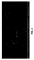
代替の酸化剤を使用するプロセスの利点は、そのようなプロセスが、上述されたプロセスのいくつかの変形において形成される意図しないナノワイヤ(「グラス(grass)」)を削減できる一方、シリコンの触媒エッチングのために金属の薄い連続層を使用しつつ、所望の100nm未満のナノワイヤをも生産することである。図4は、意図しないナノワイヤを描写する。これらの意図しないナノワイヤの回避は、それらを削減するために使用されるエッチング段階を省くと共に、このようなエッチング段階から結果として生じる、ナノ構造の角および縁の丸みも回避する。
理論によって裏づけされることを望んでいないが、本発明のこれらのプロセスにおいて使用される代替の酸化剤のいくつかは、金属を腐食せず、または、H2O2よりも遥かに小さい度合いで金属を腐食すると確信される。これが、代替の酸化剤を有するプロセスが意図しないナノワイヤの形成を回避することの理由であり得る。この理由により、H2O2が反応するほど直ちにではなく、またはより低い速度で、金属と反応することが既知の酸化剤を使用することが望ましくあり得る。
意図しないワイヤを回避するために、金属膜は、意図しない小さな穴もなく、酸素なしで清浄なシリコン表面上に堆積されることが望ましい。
本発明のプロセスのさらなる利点は、そのようなプロセスが、指定の結晶学的方向に拡張可能であることである。本発明の少なくともいくつかのプロセスでは、シリコン表面の結晶配向に関わらず、ナノワイヤは、シリコン表面に対して少なくともおおよそ垂直にエッチングされよう。これを達成するために、金属膜は、膜の一部が残りの部から隔離されたようになることを引き起こす破断または亀裂を有しないことが望ましい。金属膜は、また、十分な粘性を有し、清浄なシリコン表面上に堆積されることが望ましい。ナノワイヤの軸と基板に直角なベクトルとの間の望ましい角度は、例えば、約0.25度未満、約0.5度未満、約1度未満、または約2度未満であり得る。
本発明のプロセスでは、顕著な先細りを有するワイヤを作製することが可能であり、エッチングが進行するにつれてワイヤ直径が僅かに増大する結果を生じる。先細りはHF濃度とともに増大することが見出されている。いくつかの用途に対しては、先細りは望ましくないことがあり得る。しかしながら、光起電力の用途に対しては、先細りは有益であり得る。例えば、ほっそりとした先細りにおいて、ナノワイヤの中の自由キャリアはワイヤの縁を跳ね返り、ひいては基板の方へ下向きに伝搬する傾向にある。ナノワイヤの中よりも寧ろ基板の中に光起電力電池のp−n接合がある場合、基板に向かって増大されたこの拡散は、電池効率を増大させることが期待され得る。望ましい先細り角度は、例えば、約0.5度以下、約1度以下、約2度以下、または約4度以下、あるいは、約0.5度〜約1度、約0.5度〜約2度、または約0.5度〜約4度の範囲にあり得る。
本発明のプロセスを使用して、平均で(例えば、平均値または中央値をとる)、約150nm以下、約125nm以下、約100nm以下、約70nm以下、または約50nm以下である、ナノワイヤ直径を達成することが可能である。ナノワイヤの小さなサイズがシリコンのバンド構造を変化させる場合など、小さなナノワイヤは、ある種の用途において重要である。例えば、ナノワイヤの大多数、あるいは、少なくとも約75%、または約90%、または約95%が、上述に指示された直径など、選択される直径よりも小さい直径を有することが所望され得る。
D.応用
本発明のプロセスは、光電子デバイスに対して、シリコンを構造化するために適用され得る(参考文献(i)を参照)。そのようなプロセスは、光電子または光起電力効果を利用するデバイスにおいて採用され得、そのようなデバイスは、例えば、太陽電池(例えば、参考文献(j)および(k)を参照)、光検出器、フォトダイオード(参考文献(a)を参照)、フォトトランジスタ、光電子増倍管および光集積回路である。このプロセスを介して製造される、シリコンナノワイヤアレイまたは個別のナノワイヤは、これらの各応用の範囲内で利用され得る。
本発明のプロセスは、光電子デバイスに対して、シリコンを構造化するために適用され得る(参考文献(i)を参照)。そのようなプロセスは、光電子または光起電力効果を利用するデバイスにおいて採用され得、そのようなデバイスは、例えば、太陽電池(例えば、参考文献(j)および(k)を参照)、光検出器、フォトダイオード(参考文献(a)を参照)、フォトトランジスタ、光電子増倍管および光集積回路である。このプロセスを介して製造される、シリコンナノワイヤアレイまたは個別のナノワイヤは、これらの各応用の範囲内で利用され得る。
本発明のプロセスは、多結晶シリコンで組成される、または多結晶シリコンを含むデバイスを生産するために採用され得る。本発明は、シリコンのいかなる結晶配向をも有して使用され得るプロセスを包含する。このようなプロセスは、ポリシリコン中のナノワイヤの表面にきめを付け、および/または、ナノワイヤを形成するために使用され得る。ポリシリコンは結晶シリコンよりも安価な材料であるが、結晶粒のランダムな配向に起因して、典型的に、単結晶シリコンよりも、きめを付け、および構造化することがより困難である。本発明のプロセスは、非結晶質シリコン中にナノワイヤを形成するためにも同様に使用され得る。
シリコンナノワイヤのアレイは、ナノ構造が応力または歪みを吸収および緩和することができる場合に、シリコンが応力または歪みにさらされる用途において使用され得る。例えば、ナノワイヤは、バルクシリコンと、それに格子整合していない頂部上に成長される別の材料との間の界面の層として作用し得る。
本発明のプロセスはまた、リチウムイオン電池技術へも適用可能である。シリコンは、リチウムイオン電池におけるアノード材料として、その低い放電ポテンシャルおよび高い充電容量に起因して、望ましい候補として理解されている。その適用は過去において、イオン挿入およびイオン抽出に関連する、堆積の大きな変化に起因して、制限されている。シリコン中に起こる大量の応力および歪みは、シリコン層の劣化となる結果を生じ、非常に短い性能寿命となる結果を生じる。ナノワイヤは、これらの応力および歪みに堪えるその能力に起因して、追求されている(参考文献(l)を参照)。本発明のプロセスによって提供される、結果として生じる直径およびナノ構造間の空隙に対して多大な制御を有して、整然とした、および整列されたナノ構造を形成する能力は、リチウムイオン電池のアノードの作製において有利であろう。さらに、多孔質シリコン(ナノ細孔またはマイクロ細孔)もまた本発明のプロセスを介して製造され得るということは、リチウムイオン電池の用途に対して、イオン挿入/抽出の応力および歪みに堪えることができる、別のアノード形状の製造を可能にするであろう。
特定の型のシリコン(仮にn型)から多孔質のテンプレートまたはシリコンナノワイヤアレイを形成すること、および、p型シリコンナノワイヤの細孔を埋めるための、気相、液相、固相(VLS)プロセスのような代替技術を利用し、多種多様な光電子的(LED、光起電力)および電子的(トランジスタ)応用において利用され得る新奇のn/p接合構成となる結果を生じることが、さらに可能であろう。(VLSプロセスについてのいくつかの一般的情報については参考文献(p)を参照)。テンプレートを形成するためにシリコン基板のエッチングを触媒するAg粒子はまた、ワイヤを合成するために、細孔の基底においてワイヤ成長(例えば、VLSまたはVSSにおいて)を触媒するためにも使用され得るから、このプロセスは特に好都合である。さらに、Ag粒子はデバイスに対して電気的接触として働き得る。シリコンの他の多種多様な材料も同様に、テンプレート内部に形成され得る。数個の例は、Bi、Ge、GaN、ZnO、およびGaAsである。
本発明のプロセスは、シリコンを中間バンド光起電力材料(IBPV)へ作り換えるナノ構造を生成するために使用され得る。(参考文献(n)を参照)。特定の電子的トランジスタの強度が強化され得る場合に、シリコンはIBPVにとって優れたバンド構造を有する。これを実施する1つの態様は、参考文献(i)に記載されているように、ワイヤ直径、ドーピングおよび結晶学的配向に対して特定の制御を有して、シリコンナノワイヤの密集したアレイを形成することである。本発明のプロセスは、このようなナノワイヤアレイを製造するために使用され得る。
下記の参考文献は、本出願に関連して関心がある。

Claims (32)
- 基板の結晶シリコン表面で該基板に付着される、整列されるシリコンナノワイヤのアレイであって、
該ナノワイヤの大多数は、約150nm以下の直径を有し、該基板に対して少なくともほぼ垂直に付着され、
該アレイが付着する該結晶シリコン表面は、(100)および(111)以外の配向における結晶面である、シリコンナノワイヤのアレイ。 - 前記シリコン表面の少なくとも一部分は銀で被覆されている、請求項1に記載のアレイ。
- 前記ナノワイヤの大多数は、シリコン中の電子または正孔のコヒーレンス長未満の直径を有する、請求項1に記載のアレイ。
- 前記ナノワイヤの大多数は、シリコン中の電子または正孔のド・ブロイ波長未満の直径を有する、請求項1に記載のアレイ。
- エッチングされたナノワイヤアレイであって、該ナノワイヤの少なくとも約75%は約150nm未満の直径を有する、ナノワイヤアレイ。
- 前記エッチングは、H2O2ほど反応的ではない酸化因子の存在下で実行される、請求項5に記載のナノワイヤアレイ。
- 多結晶シリコンを備えているナノワイヤアレイ。
- 前記アレイは、主に非結晶質シリコンまたは多結晶シリコンで構成されている基板をエッチングすることによって形成される、請求項7に記載のナノワイヤアレイ。
- 前記アレイにおける前記ナノワイヤの大多数は150nm以下の直径を有する、請求項8に記載のナノワイヤアレイ。
- 構造を形成するためにシリコン含有基板をエッチングするためのプロセスであって、
(a)シリコン含有基板の表面上にナノ粒子を堆積させるステップと、
(b)エッチングが所望される場所において金属が存在してシリコンに触れ、それ以外の場所において、金属がシリコンに触れることがブロックされるか、または存在しないような態様で、該ナノ粒子およびシリコンの頂部上に金属を堆積させるステップと、
(c)該金属化された基板を、約2重量百分率から約49重量百分率までのHFと酸化因子とを含むエッチング水溶液と接触させるステップと
を包含し、
該プロセスはナノワイヤアレイを結果として生じ、該ナノワイヤアレイにおいて該ナノワイヤの平均直径は約125nm未満である、プロセス。 - 前記酸化因子は、前記エッチング水溶液を通してバブリングされる酸素ガスである、請求項10に記載のプロセス。
- 前記ステップ(b)において堆積およびパターニングされる前記金属は銀である、請求項10に記載のプロセス。
- 前記銀は約50nm未満の厚さである、請求項12に記載のプロセス。
- ステップ(a)〜ステップ(c)の結果はナノワイヤアレイであり、該ナノワイヤの平均直径は約100nm未満である、請求項10に記載のプロセス。
- ステップ(a)〜ステップ(c)の結果はナノワイヤアレイであり、該ナノワイヤの直径は約50nm未満である、請求項14に記載のプロセス。
- ステップ(a)〜ステップ(c)の結果は先細りにされているナノワイヤアレイであり、該ナノワイヤの基部は先端よりも大きい、請求項10に記載のプロセス。
- 前記シリコン含有基板の特定のエリアにおいて、前記金属が前記シリコンに触れることを防止するために、前記ナノ粒子は、該金属と該シリコン含有基板との間でバリアとして作用する、請求項10に記載のプロセス。
- 前記ナノ粒子は、エッチングが所望されない場所において前記金属を除去し、前記シリコン表面を露出するために使用される、請求項10に記載のプロセス。
- 前記金属の堆積前の前記シリコン含有基板はバルクシリコンウェハである、請求項10に記載のプロセス。
- 前記金属の堆積前の前記シリコン含有基板はsilicon−on−insulatorウェハである、請求項10に記載のプロセス。
- 前記金属の堆積前の前記シリコン含有基板は、ポリシリコンまたは微結晶質シリコンを含む、請求項10に記載のプロセス。
- 前記金属の堆積前の前記シリコン含有基板は、エピタキシャル成長されたシリコンを含む、請求項10に記載のプロセス。
- 前記金属の堆積前の前記シリコン含有基板は、シリコン上のゲルマニウム、または、シリコン上の酸化物上のゲルマニウムを含む、請求項10に記載のプロセス。
- ステップ(a)〜ステップ(c)の結果は、光電子デバイスを生産するためにさらに処理される、請求項10に記載のプロセス。
- 前記光電子デバイスは発光ダイオードである、請求項24に記載のプロセス。
- ステップ(a)〜ステップ(c)の結果は、光素子および/または導波管を生産するようにさらに処理される、請求項10に記載のプロセス。
- ステップ(a)〜ステップ(c)の結果は、光起電力デバイスまたは太陽電池デバイスを生産するようにさらに処理される、請求項10に記載のプロセス。
- ステップ(a)〜ステップ(c)によって生成されるパターンは、パターニングおよびエッチングされるシリコン含有基板の中の電子状態を混合させる、請求項10に記載のプロセス。
- 前記シリコンは、あらゆる所望の結晶学的配向を有するように選定されることが可能である、請求項10に記載のプロセス。
- リチウムイオン電池のリチウム吸収成分として、ステップ(a)〜ステップ(c)によって生成されるパターンを採用するステップをさらに包含する、請求項10に記載のプロセス。
- ステップ(b)において堆積される前記金属は、膜の一部分が残りの部分から分離されたようになることを引き起こす破断または亀裂がないように連続的である、請求項10に記載のプロセス。
- 金属で改良されたシリコンのエッチングによって作製されるシリコンナノワイヤを備えている、リチウムイオン吸収材料。
Applications Claiming Priority (5)
| Application Number | Priority Date | Filing Date | Title |
|---|---|---|---|
| US4457308P | 2008-04-14 | 2008-04-14 | |
| US61/044,573 | 2008-04-14 | ||
| US14108208P | 2008-12-29 | 2008-12-29 | |
| US61/141,082 | 2008-12-29 | ||
| PCT/US2009/040552 WO2009137241A2 (en) | 2008-04-14 | 2009-04-14 | Process for fabricating nanowire arrays |
Publications (1)
| Publication Number | Publication Date |
|---|---|
| JP2011523902A true JP2011523902A (ja) | 2011-08-25 |
Family
ID=41163224
Family Applications (1)
| Application Number | Title | Priority Date | Filing Date |
|---|---|---|---|
| JP2011505144A Pending JP2011523902A (ja) | 2008-04-14 | 2009-04-14 | ナノワイヤアレイを製造するためのプロセス |
Country Status (5)
| Country | Link |
|---|---|
| US (8) | US8143143B2 (ja) |
| EP (1) | EP2277045A4 (ja) |
| JP (1) | JP2011523902A (ja) |
| CN (1) | CN102084467A (ja) |
| WO (1) | WO2009137241A2 (ja) |
Cited By (4)
| Publication number | Priority date | Publication date | Assignee | Title |
|---|---|---|---|---|
| JP2011165403A (ja) * | 2010-02-05 | 2011-08-25 | Sony Corp | リチウムイオン二次電池用負極、リチウムイオン二次電池、電動工具、電気自動車および電力貯蔵システム |
| WO2013058091A1 (ja) * | 2011-10-17 | 2013-04-25 | 日産自動車株式会社 | 電気デバイス用負極活物質 |
| KR101327744B1 (ko) | 2012-06-22 | 2013-11-11 | 원광대학교산학협력단 | 고효율의 태양전지 제조방법 |
| JP2015146319A (ja) * | 2010-04-16 | 2015-08-13 | 株式会社半導体エネルギー研究所 | 蓄電装置 |
Families Citing this family (81)
| Publication number | Priority date | Publication date | Assignee | Title |
|---|---|---|---|---|
| WO2009137241A2 (en) | 2008-04-14 | 2009-11-12 | Bandgap Engineering, Inc. | Process for fabricating nanowire arrays |
| US8229255B2 (en) | 2008-09-04 | 2012-07-24 | Zena Technologies, Inc. | Optical waveguides in image sensors |
| US9406709B2 (en) | 2010-06-22 | 2016-08-02 | President And Fellows Of Harvard College | Methods for fabricating and using nanowires |
| US8519379B2 (en) | 2009-12-08 | 2013-08-27 | Zena Technologies, Inc. | Nanowire structured photodiode with a surrounding epitaxially grown P or N layer |
| US8889455B2 (en) | 2009-12-08 | 2014-11-18 | Zena Technologies, Inc. | Manufacturing nanowire photo-detector grown on a back-side illuminated image sensor |
| US8384007B2 (en) | 2009-10-07 | 2013-02-26 | Zena Technologies, Inc. | Nano wire based passive pixel image sensor |
| US8507840B2 (en) | 2010-12-21 | 2013-08-13 | Zena Technologies, Inc. | Vertically structured passive pixel arrays and methods for fabricating the same |
| US8890271B2 (en) | 2010-06-30 | 2014-11-18 | Zena Technologies, Inc. | Silicon nitride light pipes for image sensors |
| US9478685B2 (en) | 2014-06-23 | 2016-10-25 | Zena Technologies, Inc. | Vertical pillar structured infrared detector and fabrication method for the same |
| US8791470B2 (en) | 2009-10-05 | 2014-07-29 | Zena Technologies, Inc. | Nano structured LEDs |
| US9000353B2 (en) | 2010-06-22 | 2015-04-07 | President And Fellows Of Harvard College | Light absorption and filtering properties of vertically oriented semiconductor nano wires |
| US9515218B2 (en) | 2008-09-04 | 2016-12-06 | Zena Technologies, Inc. | Vertical pillar structured photovoltaic devices with mirrors and optical claddings |
| US8269985B2 (en) | 2009-05-26 | 2012-09-18 | Zena Technologies, Inc. | Determination of optimal diameters for nanowires |
| US8748799B2 (en) | 2010-12-14 | 2014-06-10 | Zena Technologies, Inc. | Full color single pixel including doublet or quadruplet si nanowires for image sensors |
| US8735797B2 (en) | 2009-12-08 | 2014-05-27 | Zena Technologies, Inc. | Nanowire photo-detector grown on a back-side illuminated image sensor |
| US8546742B2 (en) | 2009-06-04 | 2013-10-01 | Zena Technologies, Inc. | Array of nanowires in a single cavity with anti-reflective coating on substrate |
| US9299866B2 (en) | 2010-12-30 | 2016-03-29 | Zena Technologies, Inc. | Nanowire array based solar energy harvesting device |
| US8299472B2 (en) | 2009-12-08 | 2012-10-30 | Young-June Yu | Active pixel sensor with nanowire structured photodetectors |
| US8866065B2 (en) | 2010-12-13 | 2014-10-21 | Zena Technologies, Inc. | Nanowire arrays comprising fluorescent nanowires |
| US8835831B2 (en) | 2010-06-22 | 2014-09-16 | Zena Technologies, Inc. | Polarized light detecting device and fabrication methods of the same |
| US9343490B2 (en) | 2013-08-09 | 2016-05-17 | Zena Technologies, Inc. | Nanowire structured color filter arrays and fabrication method of the same |
| US9082673B2 (en) | 2009-10-05 | 2015-07-14 | Zena Technologies, Inc. | Passivated upstanding nanostructures and methods of making the same |
| US8274039B2 (en) | 2008-11-13 | 2012-09-25 | Zena Technologies, Inc. | Vertical waveguides with various functionality on integrated circuits |
| US8734659B2 (en) * | 2008-10-09 | 2014-05-27 | Bandgap Engineering Inc. | Process for structuring silicon |
| US20100285358A1 (en) * | 2009-05-07 | 2010-11-11 | Amprius, Inc. | Electrode Including Nanostructures for Rechargeable Cells |
| US11996550B2 (en) | 2009-05-07 | 2024-05-28 | Amprius Technologies, Inc. | Template electrode structures for depositing active materials |
| US20140370380A9 (en) * | 2009-05-07 | 2014-12-18 | Yi Cui | Core-shell high capacity nanowires for battery electrodes |
| US8450012B2 (en) | 2009-05-27 | 2013-05-28 | Amprius, Inc. | Interconnected hollow nanostructures containing high capacity active materials for use in rechargeable batteries |
| US20110024169A1 (en) * | 2009-07-28 | 2011-02-03 | Buchine Brent A | Silicon nanowire arrays on an organic conductor |
| CN105206794B (zh) | 2010-03-03 | 2018-02-23 | 安普瑞斯股份有限公司 | 用于沉积活性材料的模板电极结构 |
| US9172088B2 (en) | 2010-05-24 | 2015-10-27 | Amprius, Inc. | Multidimensional electrochemically active structures for battery electrodes |
| US9780365B2 (en) | 2010-03-03 | 2017-10-03 | Amprius, Inc. | High-capacity electrodes with active material coatings on multilayered nanostructured templates |
| US9142833B2 (en) * | 2010-06-07 | 2015-09-22 | The Regents Of The University Of California | Lithium ion batteries based on nanoporous silicon |
| TW201200465A (en) * | 2010-06-29 | 2012-01-01 | Univ Nat Central | Nano/micro-structure and fabrication method thereof |
| US20120015247A1 (en) * | 2010-07-14 | 2012-01-19 | Semiconductor Energy Laboratory Co., Ltd. | Silicon crystal body and power storage device using the silicon crystal body |
| CN101973517A (zh) * | 2010-10-21 | 2011-02-16 | 东华大学 | 一种低掺杂多孔硅纳米线阵列的制备方法 |
| US8945794B2 (en) * | 2010-11-12 | 2015-02-03 | Faris Modawar | Process for forming silver films on silicon |
| WO2012067943A1 (en) | 2010-11-15 | 2012-05-24 | Amprius, Inc. | Electrolytes for rechargeable batteries |
| US9240328B2 (en) * | 2010-11-19 | 2016-01-19 | Alphabet Energy, Inc. | Arrays of long nanostructures in semiconductor materials and methods thereof |
| US8736011B2 (en) | 2010-12-03 | 2014-05-27 | Alphabet Energy, Inc. | Low thermal conductivity matrices with embedded nanostructures and methods thereof |
| US20120181502A1 (en) * | 2011-01-18 | 2012-07-19 | Bandgap Engineering, Inc. | Method of electrically contacting nanowire arrays |
| EP2727175A4 (en) | 2011-07-01 | 2015-07-01 | Amprius Inc | ELECTRODE TEMPLATE STRUCTURES WITH IMPROVED ADHESION PROPERTIES |
| JP6025284B2 (ja) | 2011-08-19 | 2016-11-16 | 株式会社半導体エネルギー研究所 | 蓄電装置用の電極及び蓄電装置 |
| TW201330294A (zh) | 2011-09-19 | 2013-07-16 | 班蓋普工程公司 | 奈米結構區域的電性接點 |
| GB201122315D0 (en) | 2011-12-23 | 2012-02-01 | Nexeon Ltd | Etched silicon structures, method of forming etched silicon structures and uses thereof |
| WO2013123066A1 (en) | 2012-02-14 | 2013-08-22 | Bandgap Engineering, Inc. | Screen printing electrical contacts to nanowire areas |
| CN102817084B (zh) * | 2012-08-03 | 2015-06-10 | 华北电力大学 | 一种硅纳米线双层阵列结构材料的制备方法 |
| WO2014105569A1 (en) * | 2012-12-28 | 2014-07-03 | Bandgap Engineering, Inc. | Metal backed nanowire arrays |
| US9251934B2 (en) | 2013-01-11 | 2016-02-02 | Infineon Technologies Ag | Method for manufacturing a plurality of nanowires |
| CN103594535A (zh) * | 2013-01-14 | 2014-02-19 | 江苏大学 | 一种硅纳米线量子阱太阳能电池及其制备方法 |
| WO2014120830A1 (en) * | 2013-01-30 | 2014-08-07 | Bandgap Engineering, Inc. | Necklaces of silicon nanowires |
| CN103147125A (zh) * | 2013-02-27 | 2013-06-12 | 中国科学院半导体研究所 | 廉价粉末多晶硅基纳米线的制备方法 |
| US9099481B2 (en) | 2013-03-15 | 2015-08-04 | Semiconductor Components Industries, Llc | Methods of laser marking semiconductor substrates |
| US9449855B2 (en) | 2013-07-12 | 2016-09-20 | Advanced Silicon Group, Inc. | Double-etch nanowire process |
| CN105580170A (zh) | 2013-08-14 | 2016-05-11 | 得克萨斯州大学系统董事会 | 制造硅纳米线的方法和包含硅纳米线的器件 |
| WO2015038340A1 (en) * | 2013-09-10 | 2015-03-19 | Bandgap Engineering, Inc. | Metal assisted etch combined with regularizing etch |
| CA2829605C (en) | 2013-10-07 | 2016-06-14 | Springpower International Incorporated | A method for mass production of silicon nanowires and/or nanobelts, and lithium batteries and anodes using the silicon nanowires and/or nanobelts |
| CN103553046A (zh) * | 2013-10-15 | 2014-02-05 | 北京师范大学 | 一种制备多功能硅微纳米结构材料的方法 |
| CN104577077B (zh) * | 2013-10-16 | 2018-03-06 | 国家纳米科学中心 | 硅‑碳纳米复合薄膜及其制备方法和应用以及锂离子电池 |
| CN103526299A (zh) * | 2013-10-21 | 2014-01-22 | 北京师范大学 | 一种制备硅纳米结构材料的方法 |
| US9691849B2 (en) | 2014-04-10 | 2017-06-27 | Alphabet Energy, Inc. | Ultra-long silicon nanostructures, and methods of forming and transferring the same |
| TWI689126B (zh) | 2014-05-12 | 2020-03-21 | 美商安普雷斯公司 | 經結構控制之矽沈積至奈米線上 |
| DE102014107379A1 (de) * | 2014-05-26 | 2015-11-26 | Ernst-Abbe-Fachhochschule Jena | Halbleiterbauelement und Verfahren zu seiner Herstellung |
| US9324899B2 (en) | 2014-06-09 | 2016-04-26 | Natcore Technology, Inc. | Emitter diffusion conditions for black silicon |
| US20160002096A1 (en) | 2014-07-02 | 2016-01-07 | Corning Incorporated | Silicon and silica nanostructures and method of making silicon and silica nanostructures |
| WO2016063281A1 (en) | 2014-10-21 | 2016-04-28 | Ramot At Tel-Aviv University Ltd | High-capacity silicon nanowire based anode for lithium-ion batteries |
| WO2016205610A1 (en) * | 2015-06-18 | 2016-12-22 | The University Of Florida Research Foundation, Inc. | 2d tunable nanosphere lithography of nanostructures |
| CN104961094A (zh) * | 2015-07-21 | 2015-10-07 | 中国科学院上海微系统与信息技术研究所 | 基于mems工艺的细胞微阵列结构及其制备方法 |
| US10507466B2 (en) | 2016-04-27 | 2019-12-17 | International Business Machines Corporation | Metal assisted chemical etching for fabricating high aspect ratio and straight silicon nanopillar arrays for sorting applications |
| US11421345B2 (en) | 2016-08-30 | 2022-08-23 | The Regents Of University Of California | Ultrafine nanowires as highly efficient electrocatalysts |
| WO2018098506A1 (en) * | 2016-11-28 | 2018-05-31 | Sila Nanotechnologies Inc. | High-capacity battery electrodes with improved binders, construction, and performance |
| CN108459054B (zh) * | 2017-02-20 | 2020-06-19 | 天津大学 | 一种硅纳米线—聚吡咯复合材料的制备方法 |
| CN107777659B (zh) * | 2017-09-28 | 2018-08-21 | 广东工业大学 | 金属折点纳米线阵列的制备方法及其金属折点纳米线阵列 |
| US11585807B2 (en) | 2019-02-20 | 2023-02-21 | Advanced Silicon Group, Inc. | Nanotextured silicon biosensors |
| US12176526B2 (en) | 2019-02-22 | 2024-12-24 | Amprius Technologies, Inc. | Compositionally modified silicon coatings for use in a lithium ion battery anode |
| CN110010864A (zh) * | 2019-03-21 | 2019-07-12 | 中国科学院半导体研究所 | 硅-石墨烯电池负极材料及其制备方法、锂电池 |
| CN110064347B (zh) * | 2019-05-23 | 2021-09-07 | 中国石油大学(华东) | 基于仿生维管束微结构的多孔气凝胶及其制备方法和应用 |
| US11233017B2 (en) * | 2019-10-03 | 2022-01-25 | Texas Instruments Incorporated | Ex-situ manufacture of metal micro-wires and FIB placement in IC circuits |
| EP4523245A4 (en) * | 2022-05-13 | 2026-03-25 | Univ Carnegie Mellon | GROWTH OF VERTICALLY ALIGNED NANOFILES ON CONDUCTIVE SURFACES |
| CN115430450B (zh) * | 2022-08-30 | 2024-05-14 | 上海交通大学 | Rh纳米颗粒修饰III族氮氧化物Si催化剂的制备方法及其应用 |
| CN117467956A (zh) * | 2023-10-31 | 2024-01-30 | 长春理工大学 | 一种金属纳米粒子抗病毒表面及其制备方法 |
Family Cites Families (137)
| Publication number | Priority date | Publication date | Assignee | Title |
|---|---|---|---|---|
| DE2639841C3 (de) | 1976-09-03 | 1980-10-23 | Siemens Ag, 1000 Berlin Und 8000 Muenchen | Solarzelle und Verfahren zu ihrer Herstellung |
| DE3016498A1 (de) | 1980-04-29 | 1981-11-05 | Siemens AG, 1000 Berlin und 8000 München | Lichtempfindliche halbleiterbauelemente |
| DE3308269A1 (de) | 1983-03-09 | 1984-09-13 | Licentia Patent-Verwaltungs-Gmbh | Solarzelle |
| US4589191A (en) | 1983-10-20 | 1986-05-20 | Unisearch Limited | Manufacture of high efficiency solar cells |
| AU570309B2 (en) | 1984-03-26 | 1988-03-10 | Unisearch Limited | Buried contact solar cell |
| US4938568A (en) | 1988-01-05 | 1990-07-03 | Hughes Aircraft Company | Polymer dispersed liquid crystal film devices, and method of forming the same |
| US5034068A (en) | 1990-02-23 | 1991-07-23 | Spectrolab, Inc. | Photovoltaic cell having structurally supporting open conductive back electrode structure, and method of fabricating the cell |
| US5178685A (en) | 1991-06-11 | 1993-01-12 | Mobil Solar Energy Corporation | Method for forming solar cell contacts and interconnecting solar cells |
| US5221854A (en) | 1991-11-18 | 1993-06-22 | United Solar Systems Corporation | Protective layer for the back reflector of a photovoltaic device |
| US5356488A (en) | 1991-12-27 | 1994-10-18 | Rudolf Hezel | Solar cell and method for its manufacture |
| US5391235A (en) | 1992-03-31 | 1995-02-21 | Canon Kabushiki Kaisha | Solar cell module and method of manufacturing the same |
| JP2983787B2 (ja) | 1993-01-05 | 1999-11-29 | シャープ株式会社 | 表示装置の駆動回路 |
| DE69418143T2 (de) * | 1993-11-02 | 1999-08-26 | Matsushita Electric Industrial Co. | Verfahren zur Herstellung eines Aggregats von Mikro-Nadeln aus Halbleitermaterial |
| JP3563860B2 (ja) | 1996-02-23 | 2004-09-08 | シャープ株式会社 | 重合性化合物およびそれを用いた液晶表示素子 |
| US5841931A (en) | 1996-11-26 | 1998-11-24 | Massachusetts Institute Of Technology | Methods of forming polycrystalline semiconductor waveguides for optoelectronic integrated circuits, and devices formed thereby |
| DE19811878C2 (de) | 1998-03-18 | 2002-09-19 | Siemens Solar Gmbh | Verfahren und Ätzlösung zum naßchemischen pyramidalen Texturätzen von Siliziumoberflächen |
| US6063695A (en) * | 1998-11-16 | 2000-05-16 | Taiwan Semiconductor Manufacturing Company | Simplified process for the fabrication of deep clear laser marks using a photoresist mask |
| JP2000162599A (ja) | 1998-11-30 | 2000-06-16 | Sanyo Electric Co Ltd | 液晶表示装置 |
| JP4162313B2 (ja) | 1998-12-28 | 2008-10-08 | シャープ株式会社 | 液晶表示装置 |
| JP3407865B2 (ja) | 1999-02-03 | 2003-05-19 | シャープ株式会社 | 液晶表示装置 |
| JP2000250045A (ja) | 1999-02-26 | 2000-09-14 | Sharp Corp | 液晶表示装置およびその製造方法 |
| JP3619053B2 (ja) | 1999-05-21 | 2005-02-09 | キヤノン株式会社 | 光電変換装置の製造方法 |
| JP2001033815A (ja) | 1999-07-19 | 2001-02-09 | Matsushita Electric Ind Co Ltd | 液晶パネル |
| US6649824B1 (en) | 1999-09-22 | 2003-11-18 | Canon Kabushiki Kaisha | Photoelectric conversion device and method of production thereof |
| JP3879326B2 (ja) | 1999-09-30 | 2007-02-14 | セイコーエプソン株式会社 | 液晶装置の製造方法 |
| JP4606541B2 (ja) | 2000-03-23 | 2011-01-05 | シャープ株式会社 | 液晶表示装置 |
| US6334939B1 (en) | 2000-06-15 | 2002-01-01 | The University Of North Carolina At Chapel Hill | Nanostructure-based high energy capacity material |
| GB0114896D0 (en) | 2001-06-19 | 2001-08-08 | Bp Solar Ltd | Process for manufacturing a solar cell |
| JP4801848B2 (ja) | 2001-06-22 | 2011-10-26 | 東芝モバイルディスプレイ株式会社 | 液晶表示装置 |
| US6916740B2 (en) * | 2001-06-25 | 2005-07-12 | Hewlett-Packard Development Company, L.P. | Method of forming smooth polycrystalline silicon electrodes for molecular electronic devices |
| JP2003031824A (ja) | 2001-07-13 | 2003-01-31 | Sharp Corp | 太陽電池モジュール |
| US7113241B2 (en) | 2001-08-31 | 2006-09-26 | Sharp Kabushiki Kaisha | Liquid crystal display and method of manufacturing the same |
| JP4714187B2 (ja) | 2001-10-12 | 2011-06-29 | シャープ株式会社 | 液晶表示装置 |
| DE10150199A1 (de) | 2001-10-12 | 2003-04-24 | Wolfgang E Schultz | Verfahren und Schaltung zur Erkennung der Ankerlage eines Elektromagneten |
| US20030178057A1 (en) | 2001-10-24 | 2003-09-25 | Shuichi Fujii | Solar cell, manufacturing method thereof and electrode material |
| US6872645B2 (en) * | 2002-04-02 | 2005-03-29 | Nanosys, Inc. | Methods of positioning and/or orienting nanostructures |
| US7566680B2 (en) * | 2002-05-15 | 2009-07-28 | Sud-Chemie Inc. | High surface area iron material prepared from a low surface area iron metal precursor |
| JP4342200B2 (ja) | 2002-06-06 | 2009-10-14 | シャープ株式会社 | 液晶表示装置 |
| JP4248306B2 (ja) | 2002-06-17 | 2009-04-02 | シャープ株式会社 | 液晶表示装置 |
| WO2004068548A2 (en) | 2003-01-21 | 2004-08-12 | Rensselaer Polytechnic Institute | Three dimensional radiation conversion semiconductor devices |
| US6984579B2 (en) | 2003-02-27 | 2006-01-10 | Applied Materials, Inc. | Ultra low k plasma CVD nanotube/spin-on dielectrics with improved properties for advanced nanoelectronic device fabrication |
| US7279832B2 (en) * | 2003-04-01 | 2007-10-09 | Innovalight, Inc. | Phosphor materials and illumination devices made therefrom |
| US7265037B2 (en) | 2003-06-20 | 2007-09-04 | The Regents Of The University Of California | Nanowire array and nanowire solar cells and methods for forming the same |
| CN1224111C (zh) | 2003-07-04 | 2005-10-19 | 清华大学 | 硅纳米线阵列太阳能转换装置 |
| JP4434658B2 (ja) | 2003-08-08 | 2010-03-17 | キヤノン株式会社 | 構造体及びその製造方法 |
| US6986838B2 (en) | 2003-08-14 | 2006-01-17 | Johnson Research & Development Co., Inc. | Nanomachined and micromachined electrodes for electrochemical devices |
| KR100601090B1 (ko) | 2003-10-14 | 2006-07-14 | 주식회사 엘지화학 | 다공성 템플레이트를 이용하여 제조된 고표면적 전극시스템 및 이를 이용한 전기 소자 |
| US20050167655A1 (en) | 2004-01-29 | 2005-08-04 | International Business Machines Corporation | Vertical nanotube semiconductor device structures and methods of forming the same |
| WO2005094231A2 (en) | 2004-03-19 | 2005-10-13 | The Regents Of The University Of California | Methods for fabrication of positional and compositionally controlled nanostructures on substrate |
| CA2564220A1 (en) * | 2004-04-30 | 2005-12-15 | Nanosys, Inc. | Systems and methods for nanowire growth and harvesting |
| FR2880198B1 (fr) * | 2004-12-23 | 2007-07-06 | Commissariat Energie Atomique | Electrode nanostructuree pour microbatterie |
| JP4523848B2 (ja) | 2005-02-04 | 2010-08-11 | シャープ株式会社 | 液晶表示装置 |
| US20060207647A1 (en) * | 2005-03-16 | 2006-09-21 | General Electric Company | High efficiency inorganic nanorod-enhanced photovoltaic devices |
| US20060216603A1 (en) * | 2005-03-26 | 2006-09-28 | Enable Ipc | Lithium-ion rechargeable battery based on nanostructures |
| US7618838B2 (en) | 2005-04-25 | 2009-11-17 | The Research Foundation Of State University Of New York | Hybrid solar cells based on nanostructured semiconductors and organic materials |
| CN1312034C (zh) | 2005-05-20 | 2007-04-25 | 清华大学 | 单一轴向排布的单晶硅纳米线阵列制备方法 |
| US7824579B2 (en) | 2005-06-07 | 2010-11-02 | E. I. Du Pont De Nemours And Company | Aluminum thick film composition(s), electrode(s), semiconductor device(s) and methods of making thereof |
| WO2007001098A1 (en) | 2005-06-25 | 2007-01-04 | Seoul Opto Device Co., Ltd. | Nanostructure having a nitride-based quantum well and light emitting diode employing the same |
| JP4525500B2 (ja) | 2005-07-14 | 2010-08-18 | パナソニック電工株式会社 | 半導体発光素子およびそれを用いる照明装置ならびに半導体発光素子の製造方法 |
| US7589880B2 (en) | 2005-08-24 | 2009-09-15 | The Trustees Of Boston College | Apparatus and methods for manipulating light using nanoscale cometal structures |
| DE102005041877A1 (de) | 2005-09-02 | 2007-03-08 | Koynov, Svetoslav, Dr. | Verfahren zur Herstellung siliziumhaltiger Oberflächen und optoelektronische Bauelemente |
| WO2007041621A2 (en) | 2005-10-03 | 2007-04-12 | Xingsheng Sean Ling | Hybridization assisted nanopore sequencing |
| EP1772773B1 (en) * | 2005-10-06 | 2011-06-29 | STMicroelectronics Srl | Method for realizing a multispacer structure, use of said structure as a mould and method for producing circuital architectures using said mould |
| KR100759556B1 (ko) * | 2005-10-17 | 2007-09-18 | 삼성에스디아이 주식회사 | 음극 활물질, 그 제조 방법 및 이를 채용한 음극과 리튬전지 |
| US8314327B2 (en) | 2005-11-06 | 2012-11-20 | Banpil Photonics, Inc. | Photovoltaic cells based on nano or micro-scale structures |
| WO2007083362A1 (ja) | 2006-01-18 | 2007-07-26 | Fujitsu Limited | 抵抗記憶素子及びその製造方法 |
| JP2007194485A (ja) | 2006-01-20 | 2007-08-02 | Osaka Univ | 太陽電池用シリコン基板の製造方法 |
| KR20130133883A (ko) | 2006-01-20 | 2013-12-09 | 에이엠지 아이디얼캐스트 솔라 코포레이션 | 광전 변환 소자용 단결정 캐스트 실리콘 및 단결정 캐스트 실리콘 바디들을 제조하는 방법 및 장치 |
| WO2008063209A2 (en) | 2006-02-27 | 2008-05-29 | Los Alamos National Security, Llc | Optoelectronic devices utilizing materials having enhanced electronic transitions |
| US7709341B2 (en) | 2006-06-02 | 2010-05-04 | Micron Technology, Inc. | Methods of shaping vertical single crystal silicon walls and resulting structures |
| WO2008057629A2 (en) | 2006-06-05 | 2008-05-15 | The Board Of Trustees Of The University Of Illinois | Photovoltaic and photosensing devices based on arrays of aligned nanostructures |
| US8866007B2 (en) | 2006-06-07 | 2014-10-21 | California Institute Of Technology | Plasmonic photovoltaics |
| US20080038467A1 (en) * | 2006-08-11 | 2008-02-14 | Eastman Kodak Company | Nanostructured pattern method of manufacture |
| GB2442768A (en) | 2006-10-11 | 2008-04-16 | Sharp Kk | A method of encapsulating low dimensional structures |
| US7659631B2 (en) * | 2006-10-12 | 2010-02-09 | Hewlett-Packard Development Company, L.P. | Interconnection between different circuit types |
| US7776760B2 (en) | 2006-11-07 | 2010-08-17 | Nanosys, Inc. | Systems and methods for nanowire growth |
| CN100426534C (zh) | 2006-12-31 | 2008-10-15 | 高文秀 | 硅片表面金属电极制作方法 |
| US7977568B2 (en) | 2007-01-11 | 2011-07-12 | General Electric Company | Multilayered film-nanowire composite, bifacial, and tandem solar cells |
| US8257998B2 (en) | 2007-02-15 | 2012-09-04 | Massachusetts Institute Of Technology | Solar cells with textured surfaces |
| US7608530B2 (en) | 2007-03-01 | 2009-10-27 | Hewlett-Packard Development Company, L.P. | Hetero-crystalline structure and method of making same |
| KR100809248B1 (ko) | 2007-03-14 | 2008-02-29 | 삼성전기주식회사 | 반도체 이종구조 나노선을 이용한 광기전력 소자 및 그제조방법 |
| WO2008124154A2 (en) | 2007-04-09 | 2008-10-16 | Amberwave Systems Corporation | Photovoltaics on silicon |
| JP5112761B2 (ja) | 2007-06-26 | 2013-01-09 | パナソニック株式会社 | 化合物半導体素子およびそれを用いる照明装置ならびに化合物半導体素子の製造方法 |
| EP2165371B1 (en) | 2007-07-18 | 2012-02-29 | Imec | Method for producing an emitter structure and emitter structures resulting therefrom |
| US7816031B2 (en) | 2007-08-10 | 2010-10-19 | The Board Of Trustees Of The Leland Stanford Junior University | Nanowire battery methods and arrangements |
| KR101088280B1 (ko) | 2007-10-24 | 2011-11-30 | 미쓰비시덴키 가부시키가이샤 | 태양전지의 제조 방법 |
| JP5286046B2 (ja) | 2007-11-30 | 2013-09-11 | 株式会社半導体エネルギー研究所 | 光電変換装置の製造方法 |
| JP2009151204A (ja) | 2007-12-21 | 2009-07-09 | Sharp Corp | 液晶表示装置 |
| US8106289B2 (en) | 2007-12-31 | 2012-01-31 | Banpil Photonics, Inc. | Hybrid photovoltaic device |
| US8551558B2 (en) | 2008-02-29 | 2013-10-08 | International Business Machines Corporation | Techniques for enhancing efficiency of photovoltaic devices using high-aspect-ratio nanostructures |
| US8592675B2 (en) | 2008-02-29 | 2013-11-26 | International Business Machines Corporation | Photovoltaic devices with enhanced efficiencies using high-aspect-ratio nanostructures |
| US7704866B2 (en) | 2008-03-18 | 2010-04-27 | Innovalight, Inc. | Methods for forming composite nanoparticle-metal metallization contacts on a substrate |
| US20090236317A1 (en) | 2008-03-21 | 2009-09-24 | Midwest Research Institute | Anti-reflection etching of silicon surfaces catalyzed with ionic metal solutions |
| US8075792B1 (en) | 2008-03-21 | 2011-12-13 | Alliance For Sustainable Energy, Llc | Nanoparticle-based etching of silicon surfaces |
| US8273591B2 (en) | 2008-03-25 | 2012-09-25 | International Business Machines Corporation | Super lattice/quantum well nanowires |
| US20120132266A1 (en) | 2008-04-02 | 2012-05-31 | Korea Institute Of Machinery & Materials | Photoelectric conversion device using semiconductor nanomaterial |
| WO2010008425A1 (en) | 2008-04-03 | 2010-01-21 | Bandgap Engineering, Inc. | Designing the host of nano-structured optoelectronic devices to improve performance |
| US8157948B2 (en) | 2008-04-08 | 2012-04-17 | Los Alamos National Security, Llc | Method of fabricating metal- and ceramic- matrix composites and functionalized textiles |
| WO2009137241A2 (en) | 2008-04-14 | 2009-11-12 | Bandgap Engineering, Inc. | Process for fabricating nanowire arrays |
| US8491718B2 (en) | 2008-05-28 | 2013-07-23 | Karin Chaudhari | Methods of growing heteroepitaxial single crystal or large grained semiconductor films and devices thereon |
| JP2009290105A (ja) | 2008-05-30 | 2009-12-10 | Sharp Corp | 太陽電池、太陽電池の製造方法および太陽電池モジュール |
| US20100045160A1 (en) | 2008-08-20 | 2010-02-25 | Manhattan Technologies Ltd. | Multibeam doubly convergent electron gun |
| US8889455B2 (en) | 2009-12-08 | 2014-11-18 | Zena Technologies, Inc. | Manufacturing nanowire photo-detector grown on a back-side illuminated image sensor |
| JP2010087105A (ja) | 2008-09-30 | 2010-04-15 | Fujifilm Corp | 太陽電池 |
| US8734659B2 (en) | 2008-10-09 | 2014-05-27 | Bandgap Engineering Inc. | Process for structuring silicon |
| JP5612591B2 (ja) | 2008-11-14 | 2014-10-22 | バンドギャップ エンジニアリング, インコーポレイテッド | ナノ構造デバイス |
| CN101540348B (zh) | 2008-12-12 | 2011-03-16 | 北京师范大学 | 一种多用途硅微纳米结构制备技术 |
| CN101840953B (zh) | 2009-03-18 | 2011-10-12 | 中国科学院微电子研究所 | 一种制备表面混合调制晶硅太阳能电池的方法 |
| CN101882643B (zh) | 2009-05-06 | 2012-08-22 | 中国科学院微电子研究所 | 一种制作晶硅高效太阳能电池的方法 |
| US8048814B2 (en) | 2009-05-19 | 2011-11-01 | Innovalight, Inc. | Methods and apparatus for aligning a set of patterns on a silicon substrate |
| KR101033028B1 (ko) | 2009-06-25 | 2011-05-09 | 한양대학교 산학협력단 | 태양 전지 및 그 제조 방법 |
| US20110024169A1 (en) | 2009-07-28 | 2011-02-03 | Buchine Brent A | Silicon nanowire arrays on an organic conductor |
| FR2949278B1 (fr) | 2009-08-18 | 2012-11-02 | Commissariat Energie Atomique | Procede de fabrication d'un dispositif d'emission de lumiere a base de diodes electroluminescentes |
| KR101076355B1 (ko) | 2009-09-07 | 2011-10-25 | 주식회사 신성홀딩스 | 태양 전지 및 그 제조 방법 |
| DE102009043975B4 (de) | 2009-09-10 | 2012-09-13 | Q-Cells Se | Solarzelle |
| US8809093B2 (en) | 2009-11-19 | 2014-08-19 | California Institute Of Technology | Methods for fabricating self-aligning semicondutor heterostructures using silicon nanowires |
| US20110155229A1 (en) | 2009-12-30 | 2011-06-30 | Du Pont Apollo Ltd. | Solar cell and method for manufacturing the same |
| JP2011187901A (ja) | 2010-03-11 | 2011-09-22 | Canon Inc | 半導体デバイスの製造方法 |
| CN102201465A (zh) | 2010-03-26 | 2011-09-28 | 北京师范大学 | 硅微纳米结构光伏太阳能电池 |
| WO2011143341A2 (en) | 2010-05-11 | 2011-11-17 | Molecular Imprints, Inc. | Backside contact solar cell |
| US20110277825A1 (en) | 2010-05-14 | 2011-11-17 | Sierra Solar Power, Inc. | Solar cell with metal grid fabricated by electroplating |
| CN102270688A (zh) | 2010-06-01 | 2011-12-07 | 刘爱民 | 一种太阳能电池 |
| US8659037B2 (en) | 2010-06-08 | 2014-02-25 | Sundiode Inc. | Nanostructure optoelectronic device with independently controllable junctions |
| US8828765B2 (en) | 2010-06-09 | 2014-09-09 | Alliance For Sustainable Energy, Llc | Forming high efficiency silicon solar cells using density-graded anti-reflection surfaces |
| US8945794B2 (en) | 2010-11-12 | 2015-02-03 | Faris Modawar | Process for forming silver films on silicon |
| US20120181502A1 (en) | 2011-01-18 | 2012-07-19 | Bandgap Engineering, Inc. | Method of electrically contacting nanowire arrays |
| CA2815764A1 (en) | 2011-03-08 | 2012-09-13 | Alliance For Sustainable Energy, Llc | Efficient black silicon photovoltaic devices with enhanced blue response |
| CN102227002B (zh) | 2011-05-31 | 2013-01-09 | 上海交通大学 | 多晶硅纳米线太阳能电池及其制备方法 |
| KR20130030122A (ko) | 2011-09-16 | 2013-03-26 | 엘지이노텍 주식회사 | 태양전지 및 이의 제조방법 |
| TW201330294A (zh) | 2011-09-19 | 2013-07-16 | 班蓋普工程公司 | 奈米結構區域的電性接點 |
| WO2013123066A1 (en) | 2012-02-14 | 2013-08-22 | Bandgap Engineering, Inc. | Screen printing electrical contacts to nanowire areas |
| WO2014105569A1 (en) | 2012-12-28 | 2014-07-03 | Bandgap Engineering, Inc. | Metal backed nanowire arrays |
| WO2014120830A1 (en) | 2013-01-30 | 2014-08-07 | Bandgap Engineering, Inc. | Necklaces of silicon nanowires |
| US9449855B2 (en) | 2013-07-12 | 2016-09-20 | Advanced Silicon Group, Inc. | Double-etch nanowire process |
| WO2015038340A1 (en) | 2013-09-10 | 2015-03-19 | Bandgap Engineering, Inc. | Metal assisted etch combined with regularizing etch |
| US20170052182A1 (en) | 2015-08-21 | 2017-02-23 | University Of Iowa Research Foundation | Optoelectronic cartridge for cancer biomarker detection utilizing silicon nanowire arrays |
| US11585807B2 (en) | 2019-02-20 | 2023-02-21 | Advanced Silicon Group, Inc. | Nanotextured silicon biosensors |
-
2009
- 2009-04-14 WO PCT/US2009/040552 patent/WO2009137241A2/en not_active Ceased
- 2009-04-14 US US12/423,623 patent/US8143143B2/en not_active Expired - Fee Related
- 2009-04-14 JP JP2011505144A patent/JP2011523902A/ja active Pending
- 2009-04-14 EP EP09743228A patent/EP2277045A4/en not_active Withdrawn
- 2009-04-14 CN CN2009801220858A patent/CN102084467A/zh active Pending
-
2011
- 2011-11-28 US US13/305,649 patent/US8791449B2/en active Active
-
2014
- 2014-07-28 US US14/444,361 patent/US9202868B2/en active Active
-
2015
- 2015-10-27 US US14/924,273 patent/US9859366B2/en active Active
-
2017
- 2017-11-29 US US15/826,005 patent/US20180090568A1/en not_active Abandoned
-
2018
- 2018-08-03 US US16/054,457 patent/US10692971B2/en active Active
-
2020
- 2020-05-11 US US16/871,436 patent/US11355584B2/en active Active
-
2022
- 2022-04-27 US US17/660,854 patent/US20220254883A1/en not_active Abandoned
Non-Patent Citations (2)
| Title |
|---|
| JPN6013058967; Kuiquing Peng, et al.: 'Ordered silicon nanowire arrays via nanosphere lithography and metal-induced etching' Applied Physics Letters vol. 90, no. 16, 2007, 163123-163123, American Institute of Physics * |
| JPN6013058970; Zhipeng Huang, et al.: 'Fabrication of Silicon Nanowire Arrays with Controlled Diameter, Length, and Density' ADVANCED MATERIALS vol. 19, no. 5, 2007, 744-748, WILEY * |
Cited By (5)
| Publication number | Priority date | Publication date | Assignee | Title |
|---|---|---|---|---|
| JP2011165403A (ja) * | 2010-02-05 | 2011-08-25 | Sony Corp | リチウムイオン二次電池用負極、リチウムイオン二次電池、電動工具、電気自動車および電力貯蔵システム |
| JP2015146319A (ja) * | 2010-04-16 | 2015-08-13 | 株式会社半導体エネルギー研究所 | 蓄電装置 |
| WO2013058091A1 (ja) * | 2011-10-17 | 2013-04-25 | 日産自動車株式会社 | 電気デバイス用負極活物質 |
| US9979016B2 (en) | 2011-10-17 | 2018-05-22 | Nissan Motor Co., Ltd. | Negative electrode active material for electric device |
| KR101327744B1 (ko) | 2012-06-22 | 2013-11-11 | 원광대학교산학협력단 | 고효율의 태양전지 제조방법 |
Also Published As
| Publication number | Publication date |
|---|---|
| US20180090568A1 (en) | 2018-03-29 |
| US8791449B2 (en) | 2014-07-29 |
| CN102084467A (zh) | 2011-06-01 |
| US20180350908A1 (en) | 2018-12-06 |
| WO2009137241A9 (en) | 2010-04-08 |
| US20120301785A1 (en) | 2012-11-29 |
| US10692971B2 (en) | 2020-06-23 |
| US8143143B2 (en) | 2012-03-27 |
| WO2009137241A3 (en) | 2010-01-21 |
| US20220254883A1 (en) | 2022-08-11 |
| US20090256134A1 (en) | 2009-10-15 |
| US20200273950A1 (en) | 2020-08-27 |
| EP2277045A2 (en) | 2011-01-26 |
| EP2277045A4 (en) | 2012-09-19 |
| US9202868B2 (en) | 2015-12-01 |
| US20160049471A1 (en) | 2016-02-18 |
| US9859366B2 (en) | 2018-01-02 |
| US11355584B2 (en) | 2022-06-07 |
| US20140335412A1 (en) | 2014-11-13 |
| WO2009137241A2 (en) | 2009-11-12 |
Similar Documents
| Publication | Publication Date | Title |
|---|---|---|
| US20220254883A1 (en) | Process for fabricating silicon nanostructures | |
| TWI472477B (zh) | 矽奈米結構與其製造方法及應用 | |
| Li et al. | Structure and antireflection properties of SiNWs arrays form mc-Si wafer through Ag-catalyzed chemical etching | |
| Li et al. | Metal-assisted chemical etching for designable monocrystalline silicon nanostructure | |
| CN103956395B (zh) | 阵列结构绒面及其制法和应用 | |
| JP2017504179A (ja) | 結晶シリコン太陽電池の表面テクスチャ構造及びその製造方法 | |
| TWI472478B (zh) | 具有矽奈米結構的矽基板與其製造方法及應用 | |
| Leng et al. | Progress in metal-assisted chemical etching of silicon nanostructures | |
| US10079322B2 (en) | Necklaces of silicon nanowires | |
| He et al. | A simple and low-cost chemical etching method for controllable fabrication of large-scale kinked silicon nanowires | |
| Salhi et al. | Wet-chemically etched silicon nanowire: Effect of etching parameters on the morphology and optical characterizations | |
| Karbassian et al. | Formation of luminescent silicon nanowires and porous silicon by metal-assisted electroless etching | |
| US10147789B2 (en) | Process for fabricating vertically-aligned gallium arsenide semiconductor nanowire array of large area | |
| Gao et al. | Fabrication of black silicon by Ni assisted chemical etching | |
| US8945794B2 (en) | Process for forming silver films on silicon | |
| Joshi et al. | Black silicon photovoltaics: fabrication methods and properties | |
| Huo | Controlled fabrication of upright and inverted pyramid arrays of silicon via the interaction of copper ions and oxidants in hydrofluoric acid | |
| CN102650069B (zh) | 一种制备大尺寸硅孔阵列的方法 | |
| Zhang et al. | Fabrication and characterization of silicon nanostructures based on metal-assisted chemical etching | |
| HK1158821A (en) | Process for fabricating nanowire arrays | |
| Belarouci et al. | Engineering high aspect-ratio silicon nanostructures | |
| Tkach et al. | Engineering high aspect-ratio silicon nanostructures. | |
| Razak et al. | Create High-Aspect-Ratio Silicon Nanostructures Using Metal-Assisted Chemical Etching (MACE) Technique | |
| Nichkalo et al. | Morphology of Nanowire Arrays Produced by Metal-Assisted Chemical Etching on Si Wafers of Different Types: Comparative Analysis | |
| Bodian et al. | New chemical attack of Ag-catalyzed on Si in HF-H2O2-AgNO3 medium. Application to Si solar cells treatment |
Legal Events
| Date | Code | Title | Description |
|---|---|---|---|
| A621 | Written request for application examination |
Free format text: JAPANESE INTERMEDIATE CODE: A621 Effective date: 20120412 |
|
| A131 | Notification of reasons for refusal |
Free format text: JAPANESE INTERMEDIATE CODE: A131 Effective date: 20131128 |
|
| A521 | Request for written amendment filed |
Free format text: JAPANESE INTERMEDIATE CODE: A523 Effective date: 20140228 |
|
| A02 | Decision of refusal |
Free format text: JAPANESE INTERMEDIATE CODE: A02 Effective date: 20140926 |