JP2010510542A - 光学積層体を採用したカメラシステムにおける迷光の制御およびその関連方法 - Google Patents
光学積層体を採用したカメラシステムにおける迷光の制御およびその関連方法 Download PDFInfo
- Publication number
- JP2010510542A JP2010510542A JP2009537200A JP2009537200A JP2010510542A JP 2010510542 A JP2010510542 A JP 2010510542A JP 2009537200 A JP2009537200 A JP 2009537200A JP 2009537200 A JP2009537200 A JP 2009537200A JP 2010510542 A JP2010510542 A JP 2010510542A
- Authority
- JP
- Japan
- Prior art keywords
- camera system
- substrate
- optical
- stray light
- optical laminate
- Prior art date
- Legal status (The legal status is an assumption and is not a legal conclusion. Google has not performed a legal analysis and makes no representation as to the accuracy of the status listed.)
- Pending
Links
- 230000003287 optical effect Effects 0.000 title claims abstract description 112
- 238000000034 method Methods 0.000 title description 11
- 239000000758 substrate Substances 0.000 claims abstract description 154
- 230000000903 blocking effect Effects 0.000 claims abstract description 11
- 125000006850 spacer group Chemical group 0.000 claims description 12
- 239000011248 coating agent Substances 0.000 claims description 11
- 238000000576 coating method Methods 0.000 claims description 11
- 238000004519 manufacturing process Methods 0.000 claims description 3
- 238000001514 detection method Methods 0.000 abstract description 2
- 239000000463 material Substances 0.000 description 15
- 235000012431 wafers Nutrition 0.000 description 9
- 210000001747 pupil Anatomy 0.000 description 5
- 238000007789 sealing Methods 0.000 description 5
- 230000008901 benefit Effects 0.000 description 4
- 230000008569 process Effects 0.000 description 4
- 230000015572 biosynthetic process Effects 0.000 description 3
- 230000004075 alteration Effects 0.000 description 2
- 238000012634 optical imaging Methods 0.000 description 2
- 230000002093 peripheral effect Effects 0.000 description 2
- OKTJSMMVPCPJKN-UHFFFAOYSA-N Carbon Chemical compound [C] OKTJSMMVPCPJKN-UHFFFAOYSA-N 0.000 description 1
- VYPSYNLAJGMNEJ-UHFFFAOYSA-N Silicium dioxide Chemical compound O=[Si]=O VYPSYNLAJGMNEJ-UHFFFAOYSA-N 0.000 description 1
- 239000000853 adhesive Substances 0.000 description 1
- 230000001070 adhesive effect Effects 0.000 description 1
- 239000006227 byproduct Substances 0.000 description 1
- 229910052799 carbon Inorganic materials 0.000 description 1
- 239000003086 colorant Substances 0.000 description 1
- 239000000356 contaminant Substances 0.000 description 1
- 239000008393 encapsulating agent Substances 0.000 description 1
- 230000007613 environmental effect Effects 0.000 description 1
- 238000005530 etching Methods 0.000 description 1
- 239000005350 fused silica glass Substances 0.000 description 1
- 239000011521 glass Substances 0.000 description 1
- 238000011463 hyperthermic intraperitoneal chemotherapy Methods 0.000 description 1
- 238000003384 imaging method Methods 0.000 description 1
- 238000007654 immersion Methods 0.000 description 1
- 238000001746 injection moulding Methods 0.000 description 1
- 239000007788 liquid Substances 0.000 description 1
- 239000002184 metal Substances 0.000 description 1
- 238000012986 modification Methods 0.000 description 1
- 230000004048 modification Effects 0.000 description 1
- 238000000465 moulding Methods 0.000 description 1
- 238000000059 patterning Methods 0.000 description 1
- 239000011253 protective coating Substances 0.000 description 1
- 230000009467 reduction Effects 0.000 description 1
- 239000000565 sealant Substances 0.000 description 1
- 239000004065 semiconductor Substances 0.000 description 1
- 229920002050 silicone resin Polymers 0.000 description 1
- 238000007740 vapor deposition Methods 0.000 description 1
Images


Classifications
-
- G—PHYSICS
- G03—PHOTOGRAPHY; CINEMATOGRAPHY; ANALOGOUS TECHNIQUES USING WAVES OTHER THAN OPTICAL WAVES; ELECTROGRAPHY; HOLOGRAPHY
- G03B—APPARATUS OR ARRANGEMENTS FOR TAKING PHOTOGRAPHS OR FOR PROJECTING OR VIEWING THEM; APPARATUS OR ARRANGEMENTS EMPLOYING ANALOGOUS TECHNIQUES USING WAVES OTHER THAN OPTICAL WAVES; ACCESSORIES THEREFOR
- G03B17/00—Details of cameras or camera bodies; Accessories therefor
- G03B17/02—Bodies
- G03B17/12—Bodies with means for supporting objectives, supplementary lenses, filters, masks, or turrets
-
- G—PHYSICS
- G02—OPTICS
- G02B—OPTICAL ELEMENTS, SYSTEMS OR APPARATUS
- G02B27/00—Optical systems or apparatus not provided for by any of the groups G02B1/00 - G02B26/00, G02B30/00
- G02B27/0018—Optical systems or apparatus not provided for by any of the groups G02B1/00 - G02B26/00, G02B30/00 with means for preventing ghost images
-
- G—PHYSICS
- G02—OPTICS
- G02B—OPTICAL ELEMENTS, SYSTEMS OR APPARATUS
- G02B7/00—Mountings, adjusting means, or light-tight connections, for optical elements
- G02B7/02—Mountings, adjusting means, or light-tight connections, for optical elements for lenses
- G02B7/021—Mountings, adjusting means, or light-tight connections, for optical elements for lenses for more than one lens
-
- H—ELECTRICITY
- H01—ELECTRIC ELEMENTS
- H01L—SEMICONDUCTOR DEVICES NOT COVERED BY CLASS H10
- H01L27/00—Devices consisting of a plurality of semiconductor or other solid-state components formed in or on a common substrate
- H01L27/14—Devices consisting of a plurality of semiconductor or other solid-state components formed in or on a common substrate including semiconductor components sensitive to infrared radiation, light, electromagnetic radiation of shorter wavelength or corpuscular radiation and specially adapted either for the conversion of the energy of such radiation into electrical energy or for the control of electrical energy by such radiation
- H01L27/144—Devices controlled by radiation
- H01L27/146—Imager structures
- H01L27/14601—Structural or functional details thereof
- H01L27/14618—Containers
-
- H—ELECTRICITY
- H04—ELECTRIC COMMUNICATION TECHNIQUE
- H04N—PICTORIAL COMMUNICATION, e.g. TELEVISION
- H04N23/00—Cameras or camera modules comprising electronic image sensors; Control thereof
- H04N23/50—Constructional details
- H04N23/55—Optical parts specially adapted for electronic image sensors; Mounting thereof
-
- H—ELECTRICITY
- H04—ELECTRIC COMMUNICATION TECHNIQUE
- H04N—PICTORIAL COMMUNICATION, e.g. TELEVISION
- H04N23/00—Cameras or camera modules comprising electronic image sensors; Control thereof
- H04N23/57—Mechanical or electrical details of cameras or camera modules specially adapted for being embedded in other devices
-
- H—ELECTRICITY
- H05—ELECTRIC TECHNIQUES NOT OTHERWISE PROVIDED FOR
- H05K—PRINTED CIRCUITS; CASINGS OR CONSTRUCTIONAL DETAILS OF ELECTRIC APPARATUS; MANUFACTURE OF ASSEMBLAGES OF ELECTRICAL COMPONENTS
- H05K1/00—Printed circuits
- H05K1/02—Details
- H05K1/11—Printed elements for providing electric connections to or between printed circuits
- H05K1/111—Pads for surface mounting, e.g. lay-out
-
- H—ELECTRICITY
- H05—ELECTRIC TECHNIQUES NOT OTHERWISE PROVIDED FOR
- H05K—PRINTED CIRCUITS; CASINGS OR CONSTRUCTIONAL DETAILS OF ELECTRIC APPARATUS; MANUFACTURE OF ASSEMBLAGES OF ELECTRICAL COMPONENTS
- H05K1/00—Printed circuits
- H05K1/02—Details
- H05K1/14—Structural association of two or more printed circuits
-
- H—ELECTRICITY
- H01—ELECTRIC ELEMENTS
- H01L—SEMICONDUCTOR DEVICES NOT COVERED BY CLASS H10
- H01L2224/00—Indexing scheme for arrangements for connecting or disconnecting semiconductor or solid-state bodies and methods related thereto as covered by H01L24/00
- H01L2224/01—Means for bonding being attached to, or being formed on, the surface to be connected, e.g. chip-to-package, die-attach, "first-level" interconnects; Manufacturing methods related thereto
- H01L2224/42—Wire connectors; Manufacturing methods related thereto
- H01L2224/47—Structure, shape, material or disposition of the wire connectors after the connecting process
- H01L2224/48—Structure, shape, material or disposition of the wire connectors after the connecting process of an individual wire connector
- H01L2224/4805—Shape
- H01L2224/4809—Loop shape
- H01L2224/48091—Arched
Abstract
Description
Claims (36)
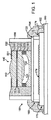
- 垂直方向において一体に固定された2つの基板と、露出した側面を有する2つの基板上にある光学部品とを有する光学的積層体と、
検出器基板上にある検出器と、
光学的積層体の少なくともいくつかの側面の上に直接的に形成された迷光遮光部材とを備えたことを特徴とするカメラシステム。 - 少なくともいくつかの側面は、光学的積層体のうちの検出器基板から最も離れた基板の側面を含むことを特徴とする請求項1に記載のカメラシステム。
- 迷光遮光部材は、光学的積層体のすべての側面の上にあることを特徴とする請求項1に記載のカメラシステム。
- 迷光遮光部材の屈折率は、上記いくつかの側面を有する基板の屈折率とほぼ同等であることを特徴とする請求項1に記載のカメラシステム。
- 光学的積層体の1つの基板が検出器基板より小さい表面積を有することを特徴とする請求項1に記載のカメラシステム。
- 迷光遮光部材は、封入部材であることを特徴とする請求項1に記載のカメラシステム。
- 迷光遮光部材は、コーティングであることを特徴とする請求項1に記載のカメラシステム。
- 迷光遮光部材は、検出器が検出できる波長光に対して不透明であることを特徴とする請求項1に記載のカメラシステム。
- 光学的積層体の基板は、同一の表面積を有することを特徴とする請求項1に記載のカメラシステム。
- 検出器基板は、少なくとも1つの方向において光学的積層体よりも大きく広がることを特徴とする請求項1に記載のカメラシステム。
- 光学的積層体よりも大きく広がる検出器基板上に接合パッドを有することを特徴とする請求項10に記載のカメラシステム。
- 接合パッドと電気的に接続される構成部品を有する基板を備えたことを特徴とする請求項11に記載のカメラシステム。
- 迷光遮光部材は、光学的積層体の上側表面から検出器基板まで延びる封入部材を有することを特徴とする請求項12に記載のカメラシステム。
- 封入部材は、接合パッド、および接合パッドと基板の間の電気的接続部品を覆うことを特徴とする請求項13に記載のカメラシステム。
- 封入部材を保持する構成部品を基板上に有することを特徴とする請求項13に記載のカメラシステム。
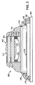
- 光学的積層体を包囲するハウジングを有することを特徴とする請求項1に記載のカメラシステム。
- 検出器基板は、少なくとも1つの方向において光学的積層体よりも大きく延びることを特徴とする請求項16に記載のカメラシステム。
- 光学的積層体よりも大きく延びる検出器基板の上にある接合パッドを有することを特徴とする請求項17に記載のカメラシステム。
- 接合パッドと電気的に接続される構成部品を有する基板を備えたことを特徴とする請求項18に記載のカメラシステム。
- 光学的積層体を包囲するハウジングが基板の下方まで延びることを特徴とする請求項19に記載のカメラシステム。
- 光学的積層体の基板は、同一の表面積を有さないことを特徴とする請求項20に記載のカメラシステム。
- ハウジングは、別の基板より広く延びる光学的積層体の上側部分を覆うように延びることを特徴とする請求項21に記載のカメラシステム。
- 迷光遮光部材は、ハウジングの上側表面にある開口部と、別の基板より広く延びる光学的積層体の上側部分との間にある封入部材を有することを特徴とする請求項22に記載のカメラシステム。
- 迷光遮光部材は、ハウジングと光学的積層体の間にある封入部材を有することを特徴とする請求項16に記載のカメラシステム。
- ハウジングは、検出器基板上のカバープレートを覆うことを特徴とする請求項16に記載のカメラシステム。
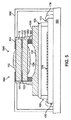
- 光学的積層体の基板は、同一の表面積を有さないことを特徴とする請求項1に記載のカメラシステム。
- 迷光遮光部材は、光学的積層体に沿った封入部材を有することを特徴とする請求項26に記載のカメラシステム。
- 光学的積層体の基板を離間させるスペーサは、露出した側面からの間隙を有することを特徴とする請求項1に記載のカメラシステム。
- 迷光遮光部材は、光学的積層体に沿った封入部材を有し、
封入部材は上記間隙を充填することを特徴とする請求項28に記載のカメラシステム。 - 検出器基板を介した電気的接続部材を有することを特徴とする請求項1に記載のカメラシステム。
- 検出器基板上のカバープレートは、少なくとも1つの方向において光学的積層体よりも大きく延びることを特徴とする請求項1に記載のカメラシステム。
- カバープレートの露出した表面の上に不透明な部材を有することを特徴とする請求項31に記載のカメラシステム。
- 不透明な部材は、迷光遮光部材と同一であることを特徴とする請求項32に記載のカメラシステム。
- カバープレートは傾斜した側壁を有し、
カバープレートの傾斜した側壁を覆う不透明部材を有することを特徴とする請求項31に記載のカメラシステム。 - 不透明部材は、迷光遮光部材と同一のものであることを特徴とする請求項34に記載のカメラシステム。
- カメラシステムの作製方法であって、
露出した側面を有する2つの基板と、これらの上にある光学部品とを有する光学的積層体を、検出器基板上にある検出器に垂直方向において一体に固定するステップと、
光学的積層体の少なくともいくつかの側面の上に迷光遮光部材を直接的に形成するステップとを有することを特徴とするカメラシステムの作製方法。
Applications Claiming Priority (2)
| Application Number | Priority Date | Filing Date | Title |
|---|---|---|---|
| US11/600,282 US20080118241A1 (en) | 2006-11-16 | 2006-11-16 | Control of stray light in camera systems employing an optics stack and associated methods |
| PCT/US2007/023961 WO2008063528A2 (en) | 2006-11-16 | 2007-11-15 | Control of stray light in camera systems employing an optics stack and associated methods |
Publications (1)
| Publication Number | Publication Date |
|---|---|
| JP2010510542A true JP2010510542A (ja) | 2010-04-02 |
Family
ID=39361289
Family Applications (1)
| Application Number | Title | Priority Date | Filing Date |
|---|---|---|---|
| JP2009537200A Pending JP2010510542A (ja) | 2006-11-16 | 2007-11-15 | 光学積層体を採用したカメラシステムにおける迷光の制御およびその関連方法 |
Country Status (7)
| Country | Link |
|---|---|
| US (1) | US20080118241A1 (ja) |
| EP (1) | EP2084896B1 (ja) |
| JP (1) | JP2010510542A (ja) |
| KR (1) | KR20090089421A (ja) |
| CN (1) | CN101606381B (ja) |
| TW (1) | TW200835306A (ja) |
| WO (1) | WO2008063528A2 (ja) |
Cited By (4)
| Publication number | Priority date | Publication date | Assignee | Title |
|---|---|---|---|---|
| JP2014081517A (ja) * | 2012-10-17 | 2014-05-08 | Mitsumi Electric Co Ltd | カメラモジュール |
| WO2014156954A1 (ja) * | 2013-03-27 | 2014-10-02 | 富士フイルム株式会社 | レンズユニット、撮像モジュール、及び電子機器 |
| US9148558B2 (en) | 2012-04-18 | 2015-09-29 | Kabushiki Kaisha Toshiba | Camera module having first and second imaging optical system controlled in relation to imaging modes and imaging method |
| WO2017195302A1 (ja) * | 2016-05-11 | 2017-11-16 | オリンパス株式会社 | レンズユニットの製造方法、及び撮像装置の製造方法 |
Families Citing this family (93)
| Publication number | Priority date | Publication date | Assignee | Title |
|---|---|---|---|---|
| US7224856B2 (en) * | 2001-10-23 | 2007-05-29 | Digital Optics Corporation | Wafer based optical chassis and associated methods |
| US7961989B2 (en) * | 2001-10-23 | 2011-06-14 | Tessera North America, Inc. | Optical chassis, camera having an optical chassis, and associated methods |
| US8546739B2 (en) * | 2007-03-30 | 2013-10-01 | Min-Chih Hsuan | Manufacturing method of wafer level chip scale package of image-sensing module |
| US7528420B2 (en) * | 2007-05-23 | 2009-05-05 | Visera Technologies Company Limited | Image sensing devices and methods for fabricating the same |
| CN101419323A (zh) * | 2007-10-22 | 2009-04-29 | 鸿富锦精密工业(深圳)有限公司 | 微型相机模组及其制作方法 |
| US8217482B2 (en) * | 2007-12-21 | 2012-07-10 | Avago Technologies General Ip (Singapore) Pte. Ltd. | Infrared proximity sensor package with reduced crosstalk |
| US9118825B2 (en) * | 2008-02-22 | 2015-08-25 | Nan Chang O-Film Optoelectronics Technology Ltd. | Attachment of wafer level optics |
| WO2009137022A1 (en) * | 2008-05-06 | 2009-11-12 | Tessera North America, Inc. | Camera system including radiation shield and method of shielding radiation |
| US8866920B2 (en) | 2008-05-20 | 2014-10-21 | Pelican Imaging Corporation | Capturing and processing of images using monolithic camera array with heterogeneous imagers |
| US11792538B2 (en) | 2008-05-20 | 2023-10-17 | Adeia Imaging Llc | Capturing and processing of images including occlusions focused on an image sensor by a lens stack array |
| EP4336447A1 (en) | 2008-05-20 | 2024-03-13 | FotoNation Limited | Capturing and processing of images using monolithic camera array with heterogeneous imagers |
| US7710667B2 (en) * | 2008-06-25 | 2010-05-04 | Aptina Imaging Corp. | Imaging module with symmetrical lens system and method of manufacture |
| GB2465607A (en) * | 2008-11-25 | 2010-05-26 | St Microelectronics | CMOS imager structures |
| US8125720B2 (en) * | 2009-03-24 | 2012-02-28 | Omnivision Technologies, Inc. | Miniature image capture lens |
| CN101872033B (zh) * | 2009-04-24 | 2014-04-30 | 鸿富锦精密工业(深圳)有限公司 | 遮光片阵列、遮光片阵列制造方法及镜头模组阵列 |
| TWM364865U (en) | 2009-05-07 | 2009-09-11 | E Pin Optical Industry Co Ltd | Miniature stacked glass lens module |
| US8420999B2 (en) * | 2009-05-08 | 2013-04-16 | Avago Technologies Ecbu Ip (Singapore) Pte. Ltd. | Metal shield and housing for optical proximity sensor with increased resistance to mechanical deformation |
| US20100295989A1 (en) * | 2009-05-22 | 2010-11-25 | Compal Electronics, Inc. | Image capturing device and manufacturing method of sealing structure |
| US9525093B2 (en) | 2009-06-30 | 2016-12-20 | Avago Technologies General Ip (Singapore) Pte. Ltd. | Infrared attenuating or blocking layer in optical proximity sensor |
| US8957380B2 (en) * | 2009-06-30 | 2015-02-17 | Avago Technologies General Ip (Singapore) Pte. Ltd. | Infrared attenuating or blocking layer in optical proximity sensor |
| US8779361B2 (en) * | 2009-06-30 | 2014-07-15 | Avago Technologies General Ip (Singapore) Pte. Ltd. | Optical proximity sensor package with molded infrared light rejection barrier and infrared pass components |
| US9419032B2 (en) * | 2009-08-14 | 2016-08-16 | Nanchang O-Film Optoelectronics Technology Ltd | Wafer level camera module with molded housing and method of manufacturing |
| US8350216B2 (en) * | 2009-09-10 | 2013-01-08 | Avago Technologies Ecbu Ip (Singapore) Pte. Ltd. | Miniaturized optical proximity sensor |
| US8143608B2 (en) * | 2009-09-10 | 2012-03-27 | Avago Technologies Ecbu Ip (Singapore) Pte. Ltd. | Package-on-package (POP) optical proximity sensor |
| US8716665B2 (en) * | 2009-09-10 | 2014-05-06 | Avago Technologies General Ip (Singapore) Pte. Ltd. | Compact optical proximity sensor with ball grid array and windowed substrate |
| US8097852B2 (en) * | 2009-09-10 | 2012-01-17 | Avago Technologies Ecbu Ip (Singapore) Pte. Ltd. | Multiple transfer molded optical proximity sensor and corresponding method |
| EP2478693B1 (en) * | 2009-09-16 | 2017-04-19 | Medigus Ltd. | Small diameter video camera heads and visualization probes and medical devices containing them |
| US20140320621A1 (en) | 2009-09-16 | 2014-10-30 | Medigus Ltd. | Small diameter video camera heads and visualization probes and medical devices containing them |
| EP2502115A4 (en) * | 2009-11-20 | 2013-11-06 | Pelican Imaging Corp | RECORDING AND PROCESSING IMAGES THROUGH A MONOLITHIC CAMERA ARRAY WITH HETEROGENIC IMAGE CONVERTER |
| US9733357B2 (en) * | 2009-11-23 | 2017-08-15 | Avago Technologies General Ip (Singapore) Pte. Ltd. | Infrared proximity sensor package with improved crosstalk isolation |
| TW201122533A (en) * | 2009-12-30 | 2011-07-01 | Hon Hai Prec Ind Co Ltd | Lens and lens module using same |
| US20120012748A1 (en) | 2010-05-12 | 2012-01-19 | Pelican Imaging Corporation | Architectures for imager arrays and array cameras |
| US8878950B2 (en) | 2010-12-14 | 2014-11-04 | Pelican Imaging Corporation | Systems and methods for synthesizing high resolution images using super-resolution processes |
| US8841597B2 (en) | 2010-12-27 | 2014-09-23 | Avago Technologies Ip (Singapore) Pte. Ltd. | Housing for optical proximity sensor |
| KR101973822B1 (ko) | 2011-05-11 | 2019-04-29 | 포토네이션 케이맨 리미티드 | 어레이 카메라 이미지 데이터를 송신 및 수신하기 위한 시스템들 및 방법들 |
| JP2014521117A (ja) | 2011-06-28 | 2014-08-25 | ペリカン イメージング コーポレイション | アレイカメラで使用するための光学配列 |
| US20130265459A1 (en) | 2011-06-28 | 2013-10-10 | Pelican Imaging Corporation | Optical arrangements for use with an array camera |
| US20130070060A1 (en) | 2011-09-19 | 2013-03-21 | Pelican Imaging Corporation | Systems and methods for determining depth from multiple views of a scene that include aliasing using hypothesized fusion |
| WO2013049699A1 (en) | 2011-09-28 | 2013-04-04 | Pelican Imaging Corporation | Systems and methods for encoding and decoding light field image files |
| EP2817955B1 (en) | 2012-02-21 | 2018-04-11 | FotoNation Cayman Limited | Systems and methods for the manipulation of captured light field image data |
| US9210392B2 (en) | 2012-05-01 | 2015-12-08 | Pelican Imaging Coporation | Camera modules patterned with pi filter groups |
| US20130341747A1 (en) * | 2012-06-20 | 2013-12-26 | Xintec Inc. | Chip package and method for forming the same |
| KR20150023907A (ko) | 2012-06-28 | 2015-03-05 | 펠리칸 이매징 코포레이션 | 결함있는 카메라 어레이들, 광학 어레이들 및 센서들을 검출하기 위한 시스템들 및 방법들 |
| US20140002674A1 (en) | 2012-06-30 | 2014-01-02 | Pelican Imaging Corporation | Systems and Methods for Manufacturing Camera Modules Using Active Alignment of Lens Stack Arrays and Sensors |
| KR102111181B1 (ko) | 2012-08-21 | 2020-05-15 | 포토내이션 리미티드 | 어레이 카메라를 사용하여 포착된 영상에서의 시차 검출 및 보정을 위한 시스템 및 방법 |
| US20140055632A1 (en) | 2012-08-23 | 2014-02-27 | Pelican Imaging Corporation | Feature based high resolution motion estimation from low resolution images captured using an array source |
| US9214013B2 (en) | 2012-09-14 | 2015-12-15 | Pelican Imaging Corporation | Systems and methods for correcting user identified artifacts in light field images |
| WO2014052974A2 (en) | 2012-09-28 | 2014-04-03 | Pelican Imaging Corporation | Generating images from light fields utilizing virtual viewpoints |
| US9143711B2 (en) | 2012-11-13 | 2015-09-22 | Pelican Imaging Corporation | Systems and methods for array camera focal plane control |
| US9462164B2 (en) | 2013-02-21 | 2016-10-04 | Pelican Imaging Corporation | Systems and methods for generating compressed light field representation data using captured light fields, array geometry, and parallax information |
| WO2014133974A1 (en) | 2013-02-24 | 2014-09-04 | Pelican Imaging Corporation | Thin form computational and modular array cameras |
| US9638883B1 (en) | 2013-03-04 | 2017-05-02 | Fotonation Cayman Limited | Passive alignment of array camera modules constructed from lens stack arrays and sensors based upon alignment information obtained during manufacture of array camera modules using an active alignment process |
| WO2014138697A1 (en) | 2013-03-08 | 2014-09-12 | Pelican Imaging Corporation | Systems and methods for high dynamic range imaging using array cameras |
| US8866912B2 (en) | 2013-03-10 | 2014-10-21 | Pelican Imaging Corporation | System and methods for calibration of an array camera using a single captured image |
| US9521416B1 (en) | 2013-03-11 | 2016-12-13 | Kip Peli P1 Lp | Systems and methods for image data compression |
| WO2014164909A1 (en) | 2013-03-13 | 2014-10-09 | Pelican Imaging Corporation | Array camera architecture implementing quantum film sensors |
| US9519972B2 (en) | 2013-03-13 | 2016-12-13 | Kip Peli P1 Lp | Systems and methods for synthesizing images from image data captured by an array camera using restricted depth of field depth maps in which depth estimation precision varies |
| US9106784B2 (en) | 2013-03-13 | 2015-08-11 | Pelican Imaging Corporation | Systems and methods for controlling aliasing in images captured by an array camera for use in super-resolution processing |
| US9124831B2 (en) | 2013-03-13 | 2015-09-01 | Pelican Imaging Corporation | System and methods for calibration of an array camera |
| US9100586B2 (en) | 2013-03-14 | 2015-08-04 | Pelican Imaging Corporation | Systems and methods for photometric normalization in array cameras |
| WO2014159779A1 (en) | 2013-03-14 | 2014-10-02 | Pelican Imaging Corporation | Systems and methods for reducing motion blur in images or video in ultra low light with array cameras |
| US9445003B1 (en) | 2013-03-15 | 2016-09-13 | Pelican Imaging Corporation | Systems and methods for synthesizing high resolution images using image deconvolution based on motion and depth information |
| US9497429B2 (en) | 2013-03-15 | 2016-11-15 | Pelican Imaging Corporation | Extended color processing on pelican array cameras |
| JP2016524125A (ja) | 2013-03-15 | 2016-08-12 | ペリカン イメージング コーポレイション | カメラアレイを用いた立体撮像のためのシステムおよび方法 |
| US10122993B2 (en) | 2013-03-15 | 2018-11-06 | Fotonation Limited | Autofocus system for a conventional camera that uses depth information from an array camera |
| US9633442B2 (en) | 2013-03-15 | 2017-04-25 | Fotonation Cayman Limited | Array cameras including an array camera module augmented with a separate camera |
| US9497370B2 (en) | 2013-03-15 | 2016-11-15 | Pelican Imaging Corporation | Array camera architecture implementing quantum dot color filters |
| CN104297887A (zh) * | 2013-07-17 | 2015-01-21 | 玉晶光电(厦门)有限公司 | 摄影镜头及用于摄影镜头的垫圈 |
| US9898856B2 (en) | 2013-09-27 | 2018-02-20 | Fotonation Cayman Limited | Systems and methods for depth-assisted perspective distortion correction |
| US9264592B2 (en) | 2013-11-07 | 2016-02-16 | Pelican Imaging Corporation | Array camera modules incorporating independently aligned lens stacks |
| WO2015074078A1 (en) | 2013-11-18 | 2015-05-21 | Pelican Imaging Corporation | Estimating depth from projected texture using camera arrays |
| WO2015081279A1 (en) | 2013-11-26 | 2015-06-04 | Pelican Imaging Corporation | Array camera configurations incorporating multiple constituent array cameras |
| WO2015134996A1 (en) | 2014-03-07 | 2015-09-11 | Pelican Imaging Corporation | System and methods for depth regularization and semiautomatic interactive matting using rgb-d images |
| US9247117B2 (en) | 2014-04-07 | 2016-01-26 | Pelican Imaging Corporation | Systems and methods for correcting for warpage of a sensor array in an array camera module by introducing warpage into a focal plane of a lens stack array |
| US9521319B2 (en) | 2014-06-18 | 2016-12-13 | Pelican Imaging Corporation | Array cameras and array camera modules including spectral filters disposed outside of a constituent image sensor |
| EP3467776A1 (en) | 2014-09-29 | 2019-04-10 | Fotonation Cayman Limited | Systems and methods for dynamic calibration of array cameras |
| EP3207416B1 (en) | 2014-10-14 | 2020-02-26 | Heptagon Micro Optics Pte. Ltd. | Optical element stack assemblies |
| US9942474B2 (en) | 2015-04-17 | 2018-04-10 | Fotonation Cayman Limited | Systems and methods for performing high speed video capture and depth estimation using array cameras |
| CN105549173A (zh) | 2016-01-28 | 2016-05-04 | 宁波舜宇光电信息有限公司 | 光学镜头和摄像模组及其组装方法 |
| US10482618B2 (en) | 2017-08-21 | 2019-11-19 | Fotonation Limited | Systems and methods for hybrid depth regularization |
| DE102017126215A1 (de) | 2017-11-09 | 2019-05-09 | Delo Industrie Klebstoffe Gmbh & Co. Kgaa | Verfahren zur Erzeugung opaker Beschichtungen, Verklebungen und Vergüsse sowie härtbare Masse zur Verwendung in dem Verfahren |
| US20200326512A1 (en) | 2017-12-21 | 2020-10-15 | Anteryon International B.V. | Lens system |
| US10935771B2 (en) | 2017-12-21 | 2021-03-02 | Anteryon International B.V. | Lens system |
| US11048067B2 (en) | 2018-05-25 | 2021-06-29 | Anteryon International B.V. | Lens system |
| DE112020004391T5 (de) | 2019-09-17 | 2022-06-02 | Boston Polarimetrics, Inc. | Systeme und verfahren zur oberflächenmodellierung unter verwendung von polarisationsmerkmalen |
| JP2022552833A (ja) | 2019-10-07 | 2022-12-20 | ボストン ポーラリメトリックス,インコーポレイティド | 偏光による面法線計測のためのシステム及び方法 |
| WO2021108002A1 (en) | 2019-11-30 | 2021-06-03 | Boston Polarimetrics, Inc. | Systems and methods for transparent object segmentation using polarization cues |
| KR20220132620A (ko) | 2020-01-29 | 2022-09-30 | 인트린식 이노베이션 엘엘씨 | 물체 포즈 검출 및 측정 시스템들을 특성화하기 위한 시스템들 및 방법들 |
| US11797863B2 (en) | 2020-01-30 | 2023-10-24 | Intrinsic Innovation Llc | Systems and methods for synthesizing data for training statistical models on different imaging modalities including polarized images |
| US11953700B2 (en) | 2020-05-27 | 2024-04-09 | Intrinsic Innovation Llc | Multi-aperture polarization optical systems using beam splitters |
| US11954886B2 (en) | 2021-04-15 | 2024-04-09 | Intrinsic Innovation Llc | Systems and methods for six-degree of freedom pose estimation of deformable objects |
| US11290658B1 (en) | 2021-04-15 | 2022-03-29 | Boston Polarimetrics, Inc. | Systems and methods for camera exposure control |
| US11689813B2 (en) | 2021-07-01 | 2023-06-27 | Intrinsic Innovation Llc | Systems and methods for high dynamic range imaging using crossed polarizers |
Citations (16)
| Publication number | Priority date | Publication date | Assignee | Title |
|---|---|---|---|---|
| JPS61129616A (ja) * | 1984-11-28 | 1986-06-17 | Olympus Optical Co Ltd | 内視鏡 |
| JPH08288484A (ja) * | 1995-04-20 | 1996-11-01 | Sony Corp | 固体撮像素子の製造方法 |
| JP2000155270A (ja) * | 1998-11-24 | 2000-06-06 | Mitsubishi Cable Ind Ltd | イメージガイド・レンズ構造体 |
| JP2001292354A (ja) * | 2000-04-07 | 2001-10-19 | Mitsubishi Electric Corp | 撮像装置 |
| JP2001292365A (ja) * | 2000-04-07 | 2001-10-19 | Mitsubishi Electric Corp | 撮像装置及びその製造方法 |
| WO2002065208A1 (fr) * | 2001-02-14 | 2002-08-22 | Arisawa Optics Co., Ltd. | Ecran de projection a reflexion |
| JP2003110891A (ja) * | 2001-09-26 | 2003-04-11 | Fuji Photo Optical Co Ltd | 撮像光学系 |
| JP2004016410A (ja) * | 2002-06-14 | 2004-01-22 | Fuji Photo Optical Co Ltd | 立体電子内視鏡装置 |
| JP2004029554A (ja) * | 2002-06-27 | 2004-01-29 | Olympus Corp | 撮像レンズユニットおよび撮像装置 |
| JP2004053648A (ja) * | 2002-07-16 | 2004-02-19 | Sharp Corp | 光通信モジュール |
| JP2005116628A (ja) * | 2003-10-03 | 2005-04-28 | Matsushita Electric Ind Co Ltd | 固体撮像装置およびその製造方法 |
| JP2005173265A (ja) * | 2003-12-11 | 2005-06-30 | Canon Inc | 光学素子、光学フィルタ装置及び光学機器 |
| JP2005295050A (ja) * | 2004-03-31 | 2005-10-20 | Miyota Kk | カメラモジュール |
| JP2005317745A (ja) * | 2004-04-28 | 2005-11-10 | Renesas Technology Corp | 固体撮像装置およびその製造方法 |
| JP2005539276A (ja) * | 2002-09-17 | 2005-12-22 | コーニンクレッカ フィリップス エレクトロニクス エヌ ヴィ | カメラ・デバイス、ならびに、カメラ・デバイスおよびウェハスケールパッケージの製造方法 |
| JP2006294720A (ja) * | 2005-04-07 | 2006-10-26 | Hitachi Maxell Ltd | カメラモジュール |
Family Cites Families (14)
| Publication number | Priority date | Publication date | Assignee | Title |
|---|---|---|---|---|
| JP3424440B2 (ja) * | 1996-06-11 | 2003-07-07 | ミノルタ株式会社 | 手ブレ補正機能を備えたカメラ |
| US5815742A (en) * | 1996-06-11 | 1998-09-29 | Minolta Co., Ltd. | Apparatus having a driven member and a drive controller therefor |
| US6686588B1 (en) * | 2001-01-16 | 2004-02-03 | Amkor Technology, Inc. | Optical module with lens integral holder |
| JP2003167102A (ja) * | 2001-12-04 | 2003-06-13 | Sony Corp | 光学素子及びその製造方法 |
| JP3675402B2 (ja) * | 2001-12-27 | 2005-07-27 | セイコーエプソン株式会社 | 光デバイス及びその製造方法、光モジュール、回路基板並びに電子機器 |
| JP2004226873A (ja) * | 2003-01-27 | 2004-08-12 | Sanyo Electric Co Ltd | カメラモジュール及びその製造方法 |
| US7880282B2 (en) * | 2003-12-18 | 2011-02-01 | Rf Module & Optical Design Ltd. | Semiconductor package with integrated heatsink and electromagnetic shield |
| DE102004001698A1 (de) * | 2004-01-13 | 2005-08-11 | Robert Bosch Gmbh | Optisches Modul |
| JP4365743B2 (ja) * | 2004-07-27 | 2009-11-18 | 富士通マイクロエレクトロニクス株式会社 | 撮像装置 |
| JP4233536B2 (ja) * | 2005-03-31 | 2009-03-04 | シャープ株式会社 | 光学装置用モジュール |
| JP4254766B2 (ja) * | 2005-09-06 | 2009-04-15 | ミツミ電機株式会社 | カメラモジュール |
| JP4794283B2 (ja) * | 2005-11-18 | 2011-10-19 | パナソニック株式会社 | 固体撮像装置 |
| KR101185881B1 (ko) * | 2006-07-17 | 2012-09-25 | 디지털옵틱스 코포레이션 이스트 | 카메라 시스템 및 관련 방법들 |
| US10949807B2 (en) | 2017-05-04 | 2021-03-16 | Servicenow, Inc. | Model building architecture and smart routing of work items |
-
2006
- 2006-11-16 US US11/600,282 patent/US20080118241A1/en not_active Abandoned
-
2007
- 2007-11-15 CN CN2007800499037A patent/CN101606381B/zh not_active Expired - Fee Related
- 2007-11-15 EP EP07840058.7A patent/EP2084896B1/en not_active Not-in-force
- 2007-11-15 KR KR1020097012362A patent/KR20090089421A/ko not_active Application Discontinuation
- 2007-11-15 JP JP2009537200A patent/JP2010510542A/ja active Pending
- 2007-11-15 WO PCT/US2007/023961 patent/WO2008063528A2/en active Application Filing
- 2007-11-16 TW TW096143796A patent/TW200835306A/zh unknown
Patent Citations (16)
| Publication number | Priority date | Publication date | Assignee | Title |
|---|---|---|---|---|
| JPS61129616A (ja) * | 1984-11-28 | 1986-06-17 | Olympus Optical Co Ltd | 内視鏡 |
| JPH08288484A (ja) * | 1995-04-20 | 1996-11-01 | Sony Corp | 固体撮像素子の製造方法 |
| JP2000155270A (ja) * | 1998-11-24 | 2000-06-06 | Mitsubishi Cable Ind Ltd | イメージガイド・レンズ構造体 |
| JP2001292354A (ja) * | 2000-04-07 | 2001-10-19 | Mitsubishi Electric Corp | 撮像装置 |
| JP2001292365A (ja) * | 2000-04-07 | 2001-10-19 | Mitsubishi Electric Corp | 撮像装置及びその製造方法 |
| WO2002065208A1 (fr) * | 2001-02-14 | 2002-08-22 | Arisawa Optics Co., Ltd. | Ecran de projection a reflexion |
| JP2003110891A (ja) * | 2001-09-26 | 2003-04-11 | Fuji Photo Optical Co Ltd | 撮像光学系 |
| JP2004016410A (ja) * | 2002-06-14 | 2004-01-22 | Fuji Photo Optical Co Ltd | 立体電子内視鏡装置 |
| JP2004029554A (ja) * | 2002-06-27 | 2004-01-29 | Olympus Corp | 撮像レンズユニットおよび撮像装置 |
| JP2004053648A (ja) * | 2002-07-16 | 2004-02-19 | Sharp Corp | 光通信モジュール |
| JP2005539276A (ja) * | 2002-09-17 | 2005-12-22 | コーニンクレッカ フィリップス エレクトロニクス エヌ ヴィ | カメラ・デバイス、ならびに、カメラ・デバイスおよびウェハスケールパッケージの製造方法 |
| JP2005116628A (ja) * | 2003-10-03 | 2005-04-28 | Matsushita Electric Ind Co Ltd | 固体撮像装置およびその製造方法 |
| JP2005173265A (ja) * | 2003-12-11 | 2005-06-30 | Canon Inc | 光学素子、光学フィルタ装置及び光学機器 |
| JP2005295050A (ja) * | 2004-03-31 | 2005-10-20 | Miyota Kk | カメラモジュール |
| JP2005317745A (ja) * | 2004-04-28 | 2005-11-10 | Renesas Technology Corp | 固体撮像装置およびその製造方法 |
| JP2006294720A (ja) * | 2005-04-07 | 2006-10-26 | Hitachi Maxell Ltd | カメラモジュール |
Cited By (5)
| Publication number | Priority date | Publication date | Assignee | Title |
|---|---|---|---|---|
| US9148558B2 (en) | 2012-04-18 | 2015-09-29 | Kabushiki Kaisha Toshiba | Camera module having first and second imaging optical system controlled in relation to imaging modes and imaging method |
| JP2014081517A (ja) * | 2012-10-17 | 2014-05-08 | Mitsumi Electric Co Ltd | カメラモジュール |
| WO2014156954A1 (ja) * | 2013-03-27 | 2014-10-02 | 富士フイルム株式会社 | レンズユニット、撮像モジュール、及び電子機器 |
| WO2017195302A1 (ja) * | 2016-05-11 | 2017-11-16 | オリンパス株式会社 | レンズユニットの製造方法、及び撮像装置の製造方法 |
| JPWO2017195302A1 (ja) * | 2016-05-11 | 2019-03-07 | オリンパス株式会社 | レンズユニットの製造方法、及び撮像装置の製造方法 |
Also Published As
| Publication number | Publication date |
|---|---|
| TW200835306A (en) | 2008-08-16 |
| EP2084896A2 (en) | 2009-08-05 |
| WO2008063528A2 (en) | 2008-05-29 |
| CN101606381A (zh) | 2009-12-16 |
| EP2084896B1 (en) | 2014-10-29 |
| US20080118241A1 (en) | 2008-05-22 |
| KR20090089421A (ko) | 2009-08-21 |
| WO2008063528A3 (en) | 2008-07-10 |
| CN101606381B (zh) | 2012-06-13 |
Similar Documents
| Publication | Publication Date | Title |
|---|---|---|
| JP2010510542A (ja) | 光学積層体を採用したカメラシステムにおける迷光の制御およびその関連方法 | |
| KR100705349B1 (ko) | 고체촬상장치, 반도체 웨이퍼 및 카메라 모듈 | |
| JP4794283B2 (ja) | 固体撮像装置 | |
| TWI686622B (zh) | 製造光學裝置的方法及將間隔件晶圓製造於光學晶圓上的方法 | |
| US7616250B2 (en) | Image capturing device | |
| EP1631060B1 (en) | Imaging device and its manufacturing method | |
| US8796798B2 (en) | Imaging module, fabricating method therefor, and imaging device | |
| US8953087B2 (en) | Camera system and associated methods | |
| JP2001351997A (ja) | 受光センサーの実装構造体およびその使用方法 | |
| JP2006222249A (ja) | 固体撮像素子パッケージ | |
| JP2008250285A (ja) | 光学部材及びそれを備えた撮像デバイス | |
| US10847664B2 (en) | Optical package and method of producing an optical package | |
| WO2020175536A1 (ja) | レンズユニットおよびカメラモジュール | |
| WO2010001524A1 (ja) | 固体撮像素子、その製造方法、及び固体撮像装置 | |
| US8986588B2 (en) | Electronic device and process for manufacturing electronic device | |
| JP2002261260A (ja) | 固体撮像装置 | |
| JP2008252043A (ja) | 固体撮像装置、固体撮像装置の製造方法およびその固体撮像装置を用いた撮影装置 | |
| WO2017110176A1 (ja) | 光学素子パッケージ | |
| WO2009137022A1 (en) | Camera system including radiation shield and method of shielding radiation | |
| US20100225799A1 (en) | Image pickup unit, method of manufacturing image pickup unit and electronic apparatus provided with image pickup unit | |
| JPS61134186A (ja) | 固体撮像デバイス | |
| JP2003017607A (ja) | 撮像素子収納用パッケージ | |
| JP2007329813A (ja) | 固体撮像装置及びこの固体撮像装置を備えた撮像装置 | |
| US20040016871A1 (en) | Image pickup device | |
| JPH04286159A (ja) | 固体撮像装置 |
Legal Events
| Date | Code | Title | Description |
|---|---|---|---|
| A131 | Notification of reasons for refusal |
Free format text: JAPANESE INTERMEDIATE CODE: A131 Effective date: 20110906 |
|
| A521 | Request for written amendment filed |
Free format text: JAPANESE INTERMEDIATE CODE: A523 Effective date: 20111206 |
|
| A131 | Notification of reasons for refusal |
Free format text: JAPANESE INTERMEDIATE CODE: A131 Effective date: 20120515 |
|
| A521 | Request for written amendment filed |
Free format text: JAPANESE INTERMEDIATE CODE: A523 Effective date: 20120725 |
|
| A02 | Decision of refusal |
Free format text: JAPANESE INTERMEDIATE CODE: A02 Effective date: 20130212 |
|
| A521 | Request for written amendment filed |
Free format text: JAPANESE INTERMEDIATE CODE: A523 Effective date: 20130522 |
|
| A911 | Transfer to examiner for re-examination before appeal (zenchi) |
Free format text: JAPANESE INTERMEDIATE CODE: A911 Effective date: 20130530 |
|
| A912 | Re-examination (zenchi) completed and case transferred to appeal board |
Free format text: JAPANESE INTERMEDIATE CODE: A912 Effective date: 20130809 |