JP2010147580A - 半導体集積回路 - Google Patents
半導体集積回路 Download PDFInfo
- Publication number
- JP2010147580A JP2010147580A JP2008319877A JP2008319877A JP2010147580A JP 2010147580 A JP2010147580 A JP 2010147580A JP 2008319877 A JP2008319877 A JP 2008319877A JP 2008319877 A JP2008319877 A JP 2008319877A JP 2010147580 A JP2010147580 A JP 2010147580A
- Authority
- JP
- Japan
- Prior art keywords
- logic
- logic element
- circuit
- error
- phase side
- Prior art date
- Legal status (The legal status is an assumption and is not a legal conclusion. Google has not performed a legal analysis and makes no representation as to the accuracy of the status listed.)
- Granted
Links
- 239000004065 semiconductor Substances 0.000 title claims abstract description 45
- 238000012545 processing Methods 0.000 claims description 10
- 238000000034 method Methods 0.000 claims description 9
- 230000008054 signal transmission Effects 0.000 claims description 8
- 238000001514 detection method Methods 0.000 abstract description 15
- 238000010586 diagram Methods 0.000 description 9
- 238000005259 measurement Methods 0.000 description 1
- 238000012544 monitoring process Methods 0.000 description 1
- 238000012546 transfer Methods 0.000 description 1
Images
Classifications
-
- H—ELECTRICITY
- H03—ELECTRONIC CIRCUITRY
- H03K—PULSE TECHNIQUE
- H03K19/00—Logic circuits, i.e. having at least two inputs acting on one output; Inverting circuits
- H03K19/007—Fail-safe circuits
Landscapes
- Logic Circuits (AREA)
- Physics & Mathematics (AREA)
- Engineering & Computer Science (AREA)
- Computer Hardware Design (AREA)
- Computing Systems (AREA)
- General Engineering & Computer Science (AREA)
- Mathematical Physics (AREA)
- Manipulation Of Pulses (AREA)
- Semiconductor Integrated Circuits (AREA)
Abstract
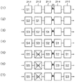
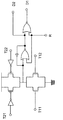
【解決手段】本発明に係る半導体集積回路は、論理素子単位でのハンドシェークを実施し、論理素子単位でのエラー発生の検出を行うことで後段の論理素子にエラー伝搬を行わないこととした。さらに、本発明に係る半導体集積回路は、各論理素子内で同一の論理回路を並列に接続し、2相で動作させることとした。
【選択図】図1
Description
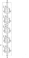
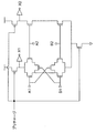
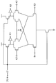
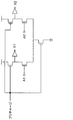
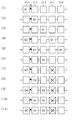
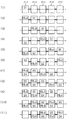
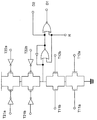
図8は、本発明に係る半導体集積回路の具体的な回路図の一例である。図8の半導体集積回路の論理ブロック35は、並列に配置された論理素子(21−11、21−12、21−13)とこれらの論理素子の出力が入力される論理素子(21−14、21−15)を備える。これらの論理素子の第一相側論理回路と第二相側論理回路は2入力2出力である。論理素子(21−11、21−12、21−13)の第一相側論理回路と第二相側論理回路にはそれぞれ入力端子32が2つ接続される。論理素子(21−11、21−12、21−13)の第一相側論理回路の一方の出力及び第二相側論理回路の一方の出力がそれぞれディテクタ(22−4、22−5、22−6)に結合される。
11、11−1〜11−5:論理回路
21、21−1〜21−5、21−11〜21−15:論理素子
22、22−1〜22−7:ディテクタ
23、23’:カウンタ
31、35:論理ブロック
32:入力端子
32’、33,33’:出力端子
A1、A2、B1、B2:入力端子
X1、X2:出力端子
R:リセット端子
T11、T12、T21、T22、T11a、T12a、T11b、T12b、T21a、T22a、T21b、T22b、D1、D2:端子
Claims (4)
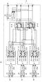
- ダイナミック回路の論理回路を持つ複数の論理素子が連結された論理ブロックと、
ハンドシェーク方式で前段の前記論理素子から後段の前記論理素子へ信号を伝送させ、前記論理素子単位で自己同期的なパイプライン動作をさせる信号伝送手段と、
前記論理素子毎の出力信号を確認し、エラーを検知したときにエラーの信号を出力した前記論理素子の動作を停止させるディテクタと、
前記論理素子へ入力する信号数又は前記論理素子が出力する信号数を計測するカウンタと、
前記ディテクタがエラーを検知したときに、前記カウンタを通過した信号数からエラーを発生した前記論理素子を特定するエラー特定手段と、
を備える半導体集積回路。 - 前記カウンタは、前記論理ブロックの入力端と出力端に配置されていることを特徴とする請求項1に記載の半導体集積回路。
- 前記論理素子のそれぞれは、第一相側と第二相側で交互に動作する並列関係にある同一の前記論理回路を持ち、非動作時に前記論理回路をリセットし、
前記信号伝送手段は、前記論理素子の第一相側の前記論理回路から出力された信号を後段の前記論理素子の第一相側の前記論理回路に結合し、前記論理素子の第二相側の前記論理回路から出力された信号を後段の前記論理素子の第二相側の前記論理回路に結合することを特徴とする請求項1又は2に記載の半導体集積回路。 - 前記論理素子が持つ第一相側と第二相側の前記論理回路は、一方が信号処理中に他方がリセット動作を行うことを特徴とする請求項3に記載の半導体集積回路。
Priority Applications (2)
| Application Number | Priority Date | Filing Date | Title |
|---|---|---|---|
| JP2008319877A JP5234957B2 (ja) | 2008-12-16 | 2008-12-16 | 半導体集積回路 |
| PCT/JP2009/070601 WO2010071063A1 (ja) | 2008-12-16 | 2009-12-09 | 半導体集積回路 |
Applications Claiming Priority (1)
| Application Number | Priority Date | Filing Date | Title |
|---|---|---|---|
| JP2008319877A JP5234957B2 (ja) | 2008-12-16 | 2008-12-16 | 半導体集積回路 |
Publications (2)
| Publication Number | Publication Date |
|---|---|
| JP2010147580A true JP2010147580A (ja) | 2010-07-01 |
| JP5234957B2 JP5234957B2 (ja) | 2013-07-10 |
Family
ID=42268734
Family Applications (1)
| Application Number | Title | Priority Date | Filing Date |
|---|---|---|---|
| JP2008319877A Expired - Fee Related JP5234957B2 (ja) | 2008-12-16 | 2008-12-16 | 半導体集積回路 |
Country Status (2)
| Country | Link |
|---|---|
| JP (1) | JP5234957B2 (ja) |
| WO (1) | WO2010071063A1 (ja) |
Citations (3)
| Publication number | Priority date | Publication date | Assignee | Title |
|---|---|---|---|---|
| JPS6095643A (ja) * | 1983-10-28 | 1985-05-29 | Fujitsu Ltd | 多段演算パイプライン診断方式 |
| JPS6429927A (en) * | 1987-07-24 | 1989-01-31 | Advantest Corp | Pipeline system arithmetic circuit |
| JPH0236436A (ja) * | 1988-07-27 | 1990-02-06 | Nec Corp | パイプラインのエラー情報記憶方式 |
-
2008
- 2008-12-16 JP JP2008319877A patent/JP5234957B2/ja not_active Expired - Fee Related
-
2009
- 2009-12-09 WO PCT/JP2009/070601 patent/WO2010071063A1/ja not_active Ceased
Patent Citations (3)
| Publication number | Priority date | Publication date | Assignee | Title |
|---|---|---|---|---|
| JPS6095643A (ja) * | 1983-10-28 | 1985-05-29 | Fujitsu Ltd | 多段演算パイプライン診断方式 |
| JPS6429927A (en) * | 1987-07-24 | 1989-01-31 | Advantest Corp | Pipeline system arithmetic circuit |
| JPH0236436A (ja) * | 1988-07-27 | 1990-02-06 | Nec Corp | パイプラインのエラー情報記憶方式 |
Also Published As
| Publication number | Publication date |
|---|---|
| JP5234957B2 (ja) | 2013-07-10 |
| WO2010071063A1 (ja) | 2010-06-24 |
Similar Documents
| Publication | Publication Date | Title |
|---|---|---|
| JPS6011495B2 (ja) | エラ−検査システム | |
| CN106796541B (zh) | 数据处理装置 | |
| JP5234957B2 (ja) | 半導体集積回路 | |
| JPH0375834A (ja) | パリティの置換装置及び方法 | |
| US10401419B2 (en) | Failure detection circuit, failure detection system and failure detection method | |
| JP3217993B2 (ja) | パリティチェック回路 | |
| JPS62293441A (ja) | デ−タ出力方式 | |
| US7996701B2 (en) | Automated clock relationship detection | |
| Chen et al. | Incorporating signature-monitoring technique in VLIW processors | |
| JPH11232210A (ja) | 情報処理装置 | |
| WO2008026283A1 (fr) | Circuit de surveillance d'horloge, appareil de traitement d'informations et procédé de surveillance d'horloge | |
| JP2606160B2 (ja) | パリティチェック回路の故障検出方式 | |
| SU959086A1 (ru) | Устройство дл диагностики двухмашинного вычислительного комплекса | |
| JP3179367B2 (ja) | 非同期データ転送装置における障害検出方式 | |
| JP5104690B2 (ja) | フォルト検出回路 | |
| JP2000261416A (ja) | 二重化データ転送回路 | |
| JPS588351A (ja) | 演算試験回路 | |
| JPH08105940A (ja) | 診断装置及び被診断装置並びにこれらを含む電子装置 | |
| JPS63281539A (ja) | 誤りデ−タ発生回路 | |
| JP2003344491A (ja) | 半導体装置の試験回路および試験方法 | |
| JPS61251938A (ja) | エラ−検出装置 | |
| JPH01188947A (ja) | データ処理装置 | |
| JP2001331384A (ja) | パッケージ間通信障害検出システム及びその方法 | |
| JPS62133534A (ja) | デ−タ処理装置のlsi | |
| JPH05127933A (ja) | 故障検出回路 |
Legal Events
| Date | Code | Title | Description |
|---|---|---|---|
| A621 | Written request for application examination |
Free format text: JAPANESE INTERMEDIATE CODE: A621 Effective date: 20111012 |
|
| TRDD | Decision of grant or rejection written | ||
| A01 | Written decision to grant a patent or to grant a registration (utility model) |
Free format text: JAPANESE INTERMEDIATE CODE: A01 Effective date: 20130312 |
|
| A61 | First payment of annual fees (during grant procedure) |
Free format text: JAPANESE INTERMEDIATE CODE: A61 Effective date: 20130322 |
|
| R150 | Certificate of patent or registration of utility model |
Free format text: JAPANESE INTERMEDIATE CODE: R150 |
|
| FPAY | Renewal fee payment (event date is renewal date of database) |
Free format text: PAYMENT UNTIL: 20160405 Year of fee payment: 3 |
|
| R250 | Receipt of annual fees |
Free format text: JAPANESE INTERMEDIATE CODE: R250 |
|
| R250 | Receipt of annual fees |
Free format text: JAPANESE INTERMEDIATE CODE: R250 |
|
| LAPS | Cancellation because of no payment of annual fees |