JP2010138433A - 半導体装置製造装置及び半導体装置製造方法 - Google Patents
半導体装置製造装置及び半導体装置製造方法 Download PDFInfo
- Publication number
- JP2010138433A JP2010138433A JP2008314219A JP2008314219A JP2010138433A JP 2010138433 A JP2010138433 A JP 2010138433A JP 2008314219 A JP2008314219 A JP 2008314219A JP 2008314219 A JP2008314219 A JP 2008314219A JP 2010138433 A JP2010138433 A JP 2010138433A
- Authority
- JP
- Japan
- Prior art keywords
- dielectrics
- semiconductor device
- cathode
- anode
- device manufacturing
- Prior art date
- Legal status (The legal status is an assumption and is not a legal conclusion. Google has not performed a legal analysis and makes no representation as to the accuracy of the status listed.)
- Pending
Links
Images


Classifications
-
- C—CHEMISTRY; METALLURGY
- C25—ELECTROLYTIC OR ELECTROPHORETIC PROCESSES; APPARATUS THEREFOR
- C25D—PROCESSES FOR THE ELECTROLYTIC OR ELECTROPHORETIC PRODUCTION OF COATINGS; ELECTROFORMING; APPARATUS THEREFOR
- C25D17/00—Constructional parts, or assemblies thereof, of cells for electrolytic coating
- C25D17/008—Current shielding devices
Landscapes
- Chemical & Material Sciences (AREA)
- Engineering & Computer Science (AREA)
- Chemical Kinetics & Catalysis (AREA)
- Electrochemistry (AREA)
- Materials Engineering (AREA)
- Metallurgy (AREA)
- Organic Chemistry (AREA)
- Electroplating Methods And Accessories (AREA)
Priority Applications (1)
| Application Number | Priority Date | Filing Date | Title |
|---|---|---|---|
| JP2008314219A JP2010138433A (ja) | 2008-12-10 | 2008-12-10 | 半導体装置製造装置及び半導体装置製造方法 |
Applications Claiming Priority (1)
| Application Number | Priority Date | Filing Date | Title |
|---|---|---|---|
| JP2008314219A JP2010138433A (ja) | 2008-12-10 | 2008-12-10 | 半導体装置製造装置及び半導体装置製造方法 |
Publications (2)
| Publication Number | Publication Date |
|---|---|
| JP2010138433A true JP2010138433A (ja) | 2010-06-24 |
| JP2010138433A5 JP2010138433A5 (https=) | 2012-01-19 |
Family
ID=42348807
Family Applications (1)
| Application Number | Title | Priority Date | Filing Date |
|---|---|---|---|
| JP2008314219A Pending JP2010138433A (ja) | 2008-12-10 | 2008-12-10 | 半導体装置製造装置及び半導体装置製造方法 |
Country Status (1)
| Country | Link |
|---|---|
| JP (1) | JP2010138433A (https=) |
Cited By (5)
| Publication number | Priority date | Publication date | Assignee | Title |
|---|---|---|---|---|
| JP2014129592A (ja) * | 2012-12-27 | 2014-07-10 | Samsung Electro-Mechanics Co Ltd | 電解メッキ遮蔽板及びこれを有する電解メッキ装置 |
| CN114262930A (zh) * | 2020-10-01 | 2022-04-01 | 株式会社荏原制作所 | 镀覆装置 |
| JP2022059561A (ja) * | 2020-10-01 | 2022-04-13 | 株式会社荏原製作所 | めっき装置 |
| CN114829681A (zh) * | 2020-11-16 | 2022-07-29 | 株式会社荏原制作所 | 板、镀敷装置和板的制造方法 |
| JP7630758B1 (ja) * | 2024-06-27 | 2025-02-17 | 株式会社荏原製作所 | めっき装置 |
Citations (7)
| Publication number | Priority date | Publication date | Assignee | Title |
|---|---|---|---|---|
| JPS5633500A (en) * | 1979-08-28 | 1981-04-03 | Fujitsu Ltd | Averaging apparatus of distribution of plating electric current |
| JPS63176500A (ja) * | 1987-01-16 | 1988-07-20 | Shinko Electric Ind Co Ltd | 電気めつき用遮蔽板 |
| JPH02145791A (ja) * | 1988-11-28 | 1990-06-05 | Eagle Ind Co Ltd | めっき装置とめっき方法およびめっき用遮蔽板 |
| JPH10140392A (ja) * | 1996-11-08 | 1998-05-26 | Hitachi Cable Ltd | 電気めっき装置 |
| JPH11246999A (ja) * | 1998-03-03 | 1999-09-14 | Ebara Corp | ウエハのメッキ方法及び装置 |
| JP2002004091A (ja) * | 2000-04-21 | 2002-01-09 | Ebara Corp | 電解処理装置及びその電場状態制御方法 |
| JP2004225129A (ja) * | 2003-01-24 | 2004-08-12 | Ebara Corp | めっき方法及びめっき装置 |
-
2008
- 2008-12-10 JP JP2008314219A patent/JP2010138433A/ja active Pending
Patent Citations (7)
| Publication number | Priority date | Publication date | Assignee | Title |
|---|---|---|---|---|
| JPS5633500A (en) * | 1979-08-28 | 1981-04-03 | Fujitsu Ltd | Averaging apparatus of distribution of plating electric current |
| JPS63176500A (ja) * | 1987-01-16 | 1988-07-20 | Shinko Electric Ind Co Ltd | 電気めつき用遮蔽板 |
| JPH02145791A (ja) * | 1988-11-28 | 1990-06-05 | Eagle Ind Co Ltd | めっき装置とめっき方法およびめっき用遮蔽板 |
| JPH10140392A (ja) * | 1996-11-08 | 1998-05-26 | Hitachi Cable Ltd | 電気めっき装置 |
| JPH11246999A (ja) * | 1998-03-03 | 1999-09-14 | Ebara Corp | ウエハのメッキ方法及び装置 |
| JP2002004091A (ja) * | 2000-04-21 | 2002-01-09 | Ebara Corp | 電解処理装置及びその電場状態制御方法 |
| JP2004225129A (ja) * | 2003-01-24 | 2004-08-12 | Ebara Corp | めっき方法及びめっき装置 |
Cited By (11)
| Publication number | Priority date | Publication date | Assignee | Title |
|---|---|---|---|---|
| JP2014129592A (ja) * | 2012-12-27 | 2014-07-10 | Samsung Electro-Mechanics Co Ltd | 電解メッキ遮蔽板及びこれを有する電解メッキ装置 |
| CN114262930A (zh) * | 2020-10-01 | 2022-04-01 | 株式会社荏原制作所 | 镀覆装置 |
| JP2022059561A (ja) * | 2020-10-01 | 2022-04-13 | 株式会社荏原製作所 | めっき装置 |
| US11542624B2 (en) * | 2020-10-01 | 2023-01-03 | Ebara Corporation | Plating apparatus |
| JP7555308B2 (ja) | 2020-10-01 | 2024-09-24 | 株式会社荏原製作所 | めっき装置 |
| TWI898052B (zh) * | 2020-10-01 | 2025-09-21 | 日商荏原製作所股份有限公司 | 鍍覆裝置 |
| CN114829681A (zh) * | 2020-11-16 | 2022-07-29 | 株式会社荏原制作所 | 板、镀敷装置和板的制造方法 |
| JP7630758B1 (ja) * | 2024-06-27 | 2025-02-17 | 株式会社荏原製作所 | めっき装置 |
| CN120418483A (zh) * | 2024-06-27 | 2025-08-01 | 株式会社荏原制作所 | 镀覆装置 |
| WO2026004077A1 (ja) * | 2024-06-27 | 2026-01-02 | 株式会社荏原製作所 | めっき装置 |
| CN120418483B (zh) * | 2024-06-27 | 2026-04-14 | 株式会社荏原制作所 | 镀覆装置 |
Similar Documents
| Publication | Publication Date | Title |
|---|---|---|
| CN106149024B (zh) | 利用离子阻性离子可穿透元件电镀金属的装置和方法 | |
| JP6427316B2 (ja) | ウェハ基板上に金属を堆積するための電気めっき装置およびウェハ基板上に電気めっきする方法 | |
| TWI550139B (zh) | 用於裁整均勻輪廓之電鍍裝置 | |
| US6919010B1 (en) | Uniform electroplating of thin metal seeded wafers using rotationally asymmetric variable anode correction | |
| KR102024380B1 (ko) | 웨이퍼 전기도금을 위한 동적 전류 분포 제어 장치 및 방법 | |
| KR102257947B1 (ko) | 도금 장치 및 도금 방법 | |
| TWI595123B (zh) | 動態電流分布控制設備及晶圓電鍍用方法 | |
| CN110512248B (zh) | 电镀设备及电镀方法 | |
| KR20120029468A (ko) | 전기도금을 위한 방법 및 장치 | |
| US9752248B2 (en) | Methods and apparatuses for dynamically tunable wafer-edge electroplating | |
| JP7237162B2 (ja) | 導電性電極を備えたセラミックシャワーヘッド | |
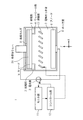
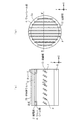
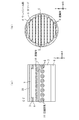
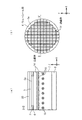
| JP2010138433A (ja) | 半導体装置製造装置及び半導体装置製造方法 | |
| US20130256623A1 (en) | Nonvolatile memory element and method of manufacturing the same | |
| KR20010040926A (ko) | 도금 장치 및 방법 | |
| JP2006505697A (ja) | 電解研磨のためのシステムと方法 | |
| TW201510291A (zh) | 非等向性高電阻離子電流源 | |
| JP3913596B2 (ja) | リチウム二次電池用電極の形成装置および形成方法 | |
| KR102043811B1 (ko) | 웨이퍼의 도금 및/또는 연마 장치 및 방법 | |
| TWI509094B (zh) | 包括嵌入金屬膜的步驟之電子元件製造方法 | |
| US20240258070A1 (en) | Plasma uniformity control system and methods | |
| JP2007177258A (ja) | プラズマ処理装置 | |
| JP2000034599A (ja) | めっき用電極およびめっき装置ならびにめっき方法 | |
| JP2006117999A (ja) | 薄膜作製方法および薄膜作製装置 |
Legal Events
| Date | Code | Title | Description |
|---|---|---|---|
| A521 | Written amendment |
Free format text: JAPANESE INTERMEDIATE CODE: A523 Effective date: 20111125 |
|
| A621 | Written request for application examination |
Free format text: JAPANESE INTERMEDIATE CODE: A621 Effective date: 20111125 |
|
| A977 | Report on retrieval |
Free format text: JAPANESE INTERMEDIATE CODE: A971007 Effective date: 20120404 |
|
| A131 | Notification of reasons for refusal |
Free format text: JAPANESE INTERMEDIATE CODE: A131 Effective date: 20130326 |
|
| A02 | Decision of refusal |
Free format text: JAPANESE INTERMEDIATE CODE: A02 Effective date: 20130718 |