JP2010094924A - 駆動回路、光プリントヘッド及び画像形成装置 - Google Patents
駆動回路、光プリントヘッド及び画像形成装置 Download PDFInfo
- Publication number
- JP2010094924A JP2010094924A JP2008268906A JP2008268906A JP2010094924A JP 2010094924 A JP2010094924 A JP 2010094924A JP 2008268906 A JP2008268906 A JP 2008268906A JP 2008268906 A JP2008268906 A JP 2008268906A JP 2010094924 A JP2010094924 A JP 2010094924A
- Authority
- JP
- Japan
- Prior art keywords
- drive
- driver
- print head
- led
- gate portion
- Prior art date
- Legal status (The legal status is an assumption and is not a legal conclusion. Google has not performed a legal analysis and makes no representation as to the accuracy of the status listed.)
- Granted
Links
Images


Classifications
-
- H—ELECTRICITY
- H10—SEMICONDUCTOR DEVICES; ELECTRIC SOLID-STATE DEVICES NOT OTHERWISE PROVIDED FOR
- H10D—INORGANIC ELECTRIC SEMICONDUCTOR DEVICES
- H10D89/00—Aspects of integrated devices not covered by groups H10D84/00 - H10D88/00
- H10D89/10—Integrated device layouts
-
- B—PERFORMING OPERATIONS; TRANSPORTING
- B41—PRINTING; LINING MACHINES; TYPEWRITERS; STAMPS
- B41J—TYPEWRITERS; SELECTIVE PRINTING MECHANISMS, i.e. MECHANISMS PRINTING OTHERWISE THAN FROM A FORME; CORRECTION OF TYPOGRAPHICAL ERRORS
- B41J2/00—Typewriters or selective printing mechanisms characterised by the printing or marking process for which they are designed
- B41J2/435—Typewriters or selective printing mechanisms characterised by the printing or marking process for which they are designed characterised by selective application of radiation to a printing material or impression-transfer material
- B41J2/447—Typewriters or selective printing mechanisms characterised by the printing or marking process for which they are designed characterised by selective application of radiation to a printing material or impression-transfer material using arrays of radiation sources
- B41J2/45—Typewriters or selective printing mechanisms characterised by the printing or marking process for which they are designed characterised by selective application of radiation to a printing material or impression-transfer material using arrays of radiation sources using light-emitting diode [LED] or laser arrays
-
- G—PHYSICS
- G03—PHOTOGRAPHY; CINEMATOGRAPHY; ANALOGOUS TECHNIQUES USING WAVES OTHER THAN OPTICAL WAVES; ELECTROGRAPHY; HOLOGRAPHY
- G03G—ELECTROGRAPHY; ELECTROPHOTOGRAPHY; MAGNETOGRAPHY
- G03G15/00—Apparatus for electrographic processes using a charge pattern
- G03G15/04—Apparatus for electrographic processes using a charge pattern for exposing, i.e. imagewise exposure by optically projecting the original image on a photoconductive recording material
- G03G15/04036—Details of illuminating systems, e.g. lamps, reflectors
- G03G15/04045—Details of illuminating systems, e.g. lamps, reflectors for exposing image information provided otherwise than by directly projecting the original image onto the photoconductive recording material, e.g. digital copiers
- G03G15/04054—Details of illuminating systems, e.g. lamps, reflectors for exposing image information provided otherwise than by directly projecting the original image onto the photoconductive recording material, e.g. digital copiers by LED arrays
-
- G—PHYSICS
- G03—PHOTOGRAPHY; CINEMATOGRAPHY; ANALOGOUS TECHNIQUES USING WAVES OTHER THAN OPTICAL WAVES; ELECTROGRAPHY; HOLOGRAPHY
- G03G—ELECTROGRAPHY; ELECTROPHOTOGRAPHY; MAGNETOGRAPHY
- G03G15/00—Apparatus for electrographic processes using a charge pattern
- G03G15/22—Apparatus for electrographic processes using a charge pattern involving the combination of more than one step according to groups G03G13/02 - G03G13/20
- G03G15/32—Apparatus for electrographic processes using a charge pattern involving the combination of more than one step according to groups G03G13/02 - G03G13/20 in which the charge pattern is formed dotwise, e.g. by a thermal head
- G03G15/326—Apparatus for electrographic processes using a charge pattern involving the combination of more than one step according to groups G03G13/02 - G03G13/20 in which the charge pattern is formed dotwise, e.g. by a thermal head by application of light, e.g. using a LED array
-
- H—ELECTRICITY
- H03—ELECTRONIC CIRCUITRY
- H03K—PULSE TECHNIQUE
- H03K17/00—Electronic switching or gating, i.e. not by contact-making and –breaking
- H03K17/12—Modifications for increasing the maximum permissible switched current
- H03K17/122—Modifications for increasing the maximum permissible switched current in field-effect transistor switches
-
- H—ELECTRICITY
- H10—SEMICONDUCTOR DEVICES; ELECTRIC SOLID-STATE DEVICES NOT OTHERWISE PROVIDED FOR
- H10D—INORGANIC ELECTRIC SEMICONDUCTOR DEVICES
- H10D64/00—Electrodes of devices having potential barriers
- H10D64/20—Electrodes characterised by their shapes, relative sizes or dispositions
- H10D64/27—Electrodes not carrying the current to be rectified, amplified, oscillated or switched, e.g. gates
- H10D64/311—Gate electrodes for field-effect devices
- H10D64/411—Gate electrodes for field-effect devices for FETs
- H10D64/511—Gate electrodes for field-effect devices for FETs for IGFETs
- H10D64/517—Gate electrodes for field-effect devices for FETs for IGFETs characterised by the conducting layers
- H10D64/519—Gate electrodes for field-effect devices for FETs for IGFETs characterised by the conducting layers characterised by their top-view geometrical layouts
-
- H—ELECTRICITY
- H10—SEMICONDUCTOR DEVICES; ELECTRIC SOLID-STATE DEVICES NOT OTHERWISE PROVIDED FOR
- H10D—INORGANIC ELECTRIC SEMICONDUCTOR DEVICES
- H10D84/00—Integrated devices formed in or on semiconductor substrates that comprise only semiconducting layers, e.g. on Si wafers or on GaAs-on-Si wafers
- H10D84/90—Masterslice integrated circuits
- H10D84/998—Input and output buffer/driver structures
-
- H—ELECTRICITY
- H10—SEMICONDUCTOR DEVICES; ELECTRIC SOLID-STATE DEVICES NOT OTHERWISE PROVIDED FOR
- H10H—INORGANIC LIGHT-EMITTING SEMICONDUCTOR DEVICES HAVING POTENTIAL BARRIERS
- H10H29/00—Integrated devices, or assemblies of multiple devices, comprising at least one light-emitting semiconductor element covered by group H10H20/00
- H10H29/10—Integrated devices comprising at least one light-emitting semiconductor component covered by group H10H20/00
- H10H29/14—Integrated devices comprising at least one light-emitting semiconductor component covered by group H10H20/00 comprising multiple light-emitting semiconductor components
-
- H10W90/753—
Landscapes
- Physics & Mathematics (AREA)
- General Physics & Mathematics (AREA)
- Optics & Photonics (AREA)
- Health & Medical Sciences (AREA)
- General Health & Medical Sciences (AREA)
- Toxicology (AREA)
- Printers Or Recording Devices Using Electromagnetic And Radiation Means (AREA)
- Facsimile Heads (AREA)
- Semiconductor Integrated Circuits (AREA)
- Metal-Oxide And Bipolar Metal-Oxide Semiconductor Integrated Circuits (AREA)
Abstract
【解決手段】LEDプリントヘッドに搭載されるドライバIC中の複数のLED駆動回路110において、駆動トランジスタであるPMOS118〜122のゲート118G〜121G,122−1G〜122−4GをLEDアレイ方向(X軸方向)に並列に配置して、PMOSのチャネルがLEDアレイ方向に対して直交する方向(Y軸方向)となるように配置し、ドレイン電流をY軸方向に流す構成にしている。そのため、低温雰囲気中であってもドライバIC端部とドライバIC中心部との駆動電流の差が小さくなり、ドライバIC内での駆動電流のばらつきを改善できる。これにより、画像形成装置における印刷濃度のむらを解消できて印刷品位を向上できる。
【選択図】図1
Description
図2は、本発明の実施例1における画像形成装置を示す概略の構成図である。
先ず、用紙カセット21に堆積した状態で収納されている用紙20が、ホッピングローラ22によって、上から1枚ずつ分離されて搬送される。続いて、この用紙20は、搬送ローラ25、レジストローラ26及びピンチローラ23、24に挟持されて、プロセスユニット10−1の感光体ドラム11と転写ローラ27の間に搬送される。その後、用紙20は、感光体ドラム61及び転写ローラ27に挟持され、その記録面にトナー像が転写されると同時に感光体ドラム10−1の回転によって搬送される。同様にして、用紙20は、順次プロセスユニット10−2〜10−4を通過し、その通過過程で、各光プリントヘッド13により形成された静電潜像を各現像装置14によって現像した各色のトナー像が、その記録面に順次転写されて重ね合わされる。
図3は、図2中のLEDプリントヘッドの構成を示す概略の断面図である。
図4は、図2の電子写真プリンタにおけるプリンタ制御回路の構成を示すブロック図である。
印刷制御部40は、上位コントローラからの制御信号SGlによって印刷指示を受信すると、先ず、温度センサ49によって定着装置28内の加熱ローラ28aが使用可能な温度範囲にあるか否かを検出し、温度範囲になければ加熱ローラ28aに通電し、使用可能な温度まで定着装置28を加熱する。次に、ドライバ41を介して現像・転写プロセス用モータ42を回転させ、同時にチャージ信号SGCによって帯電用高圧電源50をオンにし、現像装置14の帯電を行う。
図5は、図4中の各プロセッサユニット10−1〜10−4における各LEDプリントヘッド13を示す構成図である。
図5に示す構成においては、印刷データ信号HD−DATA3〜HD−DATA0は4本であり、隣接するLED8個のうち、奇数番目同士あるいは偶数番目同士の4画素分のデータをクロック信号HD−CLK毎に同時に送出する構成になっている。このため、図4の印刷制御部40から出力される印刷データ信号HD−DATA3〜HD−DATA0は、クロック信号HD−CLKと共にドライバIC100−1に入力され、前記の4992ドット分のビットデータDATAI0〜DATAI3,・・・が後述する各ドライバIC100−1,・・・内のフリッププロップ回路(以下「FF」という、)から成るシフトレジスタ中を順次転送される。
図6は、図5中のチップ状のドライバIC100(=100−1、1002,・・・)における構成を示す平面図である。この図6には、1チップ分のドライバIC100におけるの端子パッド部と内部回路の配置状況が示されている。
図7は、図5中のドライバIC100の詳細な構成を示すブロック図である。
図8は、図7中のLEDの駆動回路110(=110−1〜110−96)を示す回路図である。
印刷データであるラッチ回路103からのビットデータEがオン(即ち、低レベル(以下「Lレベル」という。)であり、制御回路130からのオン/オフ制御信号SがLレベルとなって駆動オンを指令している時、NOR回路111の出力はHレベルとなる。この時、マルチプレクサ105からの補正データQ3〜QOに従い、NAND回路112〜115の出力信号と、PMOS116及びNMOS117により構成されるインバータの出力とは、電源電圧VDDレベルあるいは制御電圧Vcontレベルとなる。
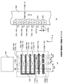
図1(a)、(b)は、本発明の実施例1における図8中の駆動トランジスタであるPMOS118〜122を示す構成図であり、同図(a)は平面図、及び、同図(b)は同図(a)中のA1−A2線断面図である。
Wl=2*WO
W2=4*WO
W3=8*WO
図9(a)〜(c)は、図3中のLEDプリントヘッド基板ユニットを示す構成図であり、同図(a)は平面図、同図(b)はその平面図の一部の拡大図、及び、同図(c)は同図(b)に対比するように描かれた断面図である。
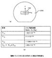
図10(a)、(b)は、図1、図8及び図9における駆動トランジスタであるPMOS118〜122に応力が加わった場合の特性変化(ドレイン電流の変動)を説明するための図であり、同図(a)は、シリコンウェハ上にドライバIC100を形成する時のドライバIC100の配列方向を示す図、及び同図(b)は、その関係式及びその数値を示す図である。
ε=△L/L
であるが、力と直交する方向のひずみε’は、
ε’=(d−d’)/d
である。力の方向のひずみεと、力と直交する方向のひずみε’との比は、物質により定まる定数であって、ポアソソン比νと呼ばれ、
σ=Eε
の関係があり、Eはヤング率とよばれ、図11(a)のX軸方向、Y軸方向について、
E≒170[GPa]
であることが知られている。
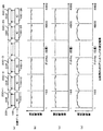
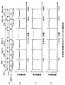
図11−1(a)〜(d)及び図11−2(a)〜(d)は、従来の構成である比較例と本実施例1のLEDプリントヘッドにおける測定結果を示す図であり、図11−1(a)〜(d)は、比較例のLEDプリントヘッドにおいてドット毎の駆動電流を周囲温度を変えて測定した結果を模式的に示す図、図11−2(a)〜(d)は、本実施例1における図9及び図10の構成を備えるLEDプリントヘッド13においてドット毎の駆動電流を周囲温度を変えて測定した結果を模式的に示す図である。
温度変化によってドライバIC100における駆動電流にばらつきが生じると、ドライバIC100により駆動されるLEDの光量むらを生じ、それを用いる画像形成装置の印刷結果に濃度むらとなって現れ、印刷品位を著しく低下させることとなって好ましくない。それに加えて、LEDプリントヘッド13においては、各LEDの製造ばらつきに起因して発光効率がばらつくため、これをLEDプリントヘッド13の製造段階で補正するための光量補正機能を備えるのが通例である。
図12は、図8中の駆動トランジスタであるPMOS118〜122の平面図を示す本発明の実施例2の構成図であり、実施例1の駆動トランジスタの平面図を示す図1(a)中の要素と共通の要素には共通の符号が付されている。
Wl=2*WO
W2=4*WO
W3=8*WO
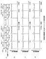
図13(a)〜(d)は、本発明の実施例2のLEDプリントヘッドにおいて低温雰囲気中(約20℃)におけるドット毎の駆動電流の測定結果を模式的に示す図であり、実施例1を示す図11−2(a)〜(d)中の要素と共通の要素には共通の符号が付されている。
本実施例2における図7中の駆動回路110及びこれを用いた図4中のLEDプリントヘッド13によれば、低温雰囲気中であっても各ドライバIC端部と各ドライバIC中心部との駆動電流の差が比較例のものより小さくなり、ドライバIC内での駆動電流のばらつきを改善することができる。従って、実施例1と略同様に、印刷濃度のむらを解消できて、印刷品位に優れた画像形成装置1を実現できる。
図14は、実施例2における図12の駆動トランジスタの構成の変形例を示す平面図であり、図12中の要素と共通の要素には共通の符号が付されている。
Wl=2*WO
W2=4*WO
W3=8*WO
図15は、図8中の駆動トランジスタであるPMOS118〜122の平面図を示す本発明の実施例3の構成図であり、実施例1の駆動トランジスタの平面図を示す図1(a)中の要素と共通の要素には共通の符号が付されている。
Wl=2*WO
W2=4*WO
W3=8*WO
図16(a)〜(d)は、本発明の実施例3のLEDプリントヘッドにおいて低温雰囲気中(約−20℃)におけるドット毎の駆動電流の測定結果を模式的に示す図であり、実施例1を示す図11−2(a)〜(d)中の要素と共通の要素には共通の符号が付されている。
本実施例3における図7中の駆動回路110及びこれを用いた図4中のLEDプリントヘッド13によれば、低温雰囲気中であっても各ドライバIC端部と各ドライバIC中心部との駆動電流の差が比較例のものより小さくなり、ドライバIC内での駆動電流のばらつきを改善することができる。従って、実施例1と略同様に、印刷濃度のむらを解消できて、印刷品位に優れた画像形成装置1を実現できる。
図17は、図8中の駆動トランジスタであるPMOS118〜122の平面図を示す本発明の実施例4の構成図であり、実施例1の駆動トランジスタの平面図を示す図1(a)中の要素と共通の要素には共通の符号が付されている。
図18(a)〜(d)は、本発明の実施例4のLEDプリントヘッドにおいて低温雰囲気中(約−20℃)におけるドット毎の駆動電流の測定結果を模式的に示す図であり、実施例1を示す図11−2(a)〜(d)中の要素と共通の要素には共通の符号が付されている。
本実施例4における図7中の駆動回路110及びこれを用いた図4中のLEDプリントヘッド13によれば、低温雰囲気中であっても各ドライバIC端部と各ドライバIC中心部との駆動電流の差が比較例のものより小さくなり、ドライバIC内での駆動電流のばらつきを改善することができる。従って、実施例1と略同様に、印刷濃度のむらを解消できて、印刷品位に優れた画像形成装置1を実現できる。
本発明は、上記実施例1〜4に限定されず、種々の利用形態や変形が可能である。この利用形態や変形例としては、例えば、次の(a)〜(d)のようなものがある。
13 LEDプリントヘッド
13b プリント基板
13e ロッドレンズアレイ
100 ドライバIC
110,110−1〜110−96 駆動回路
118〜122 PMOS
200,200−1〜200−96 LEDアレイ
Claims (11)
- 複数の被駆動素子に駆動電流を供給する駆動トランジスタを有する駆動回路において、
前記駆動トランジスタは、前記被駆動素子の配列方向に略等しい向きに延設された第1のゲート部を有することを特徴とする駆動回路。 - 前記第1のゲート部と同じ半導体層に形成された一体化ゲート部を構成し、前記被駆動素子の配列方向とは異なる向きに延設された第2のゲート部を有することを特徴とする請求項1記載の駆動回路。
- 前記第2のゲート部は、前記第1のゲート部と略直交する方向に延設されていることを特徴とする請求項2記載の駆動回路。
- 前記一体化ゲート部は、略L字状であることを特徴とする請求項2記載の駆動回路。
- 前記一体化ゲート部は、略U字状であることを特徴とする請求項2記載の駆動回路。
- 前記一体化ゲート部は、前記第1のゲート部と前記第2のゲート部とにより囲まれる閉領域を有することを特徴とする請求項2記載の駆動回路。
- 前記閉領域は前記第1のゲート部又は前記第2のゲート部により分離された複数の領域から成ることを特徴とする請求項6記載の駆動回路。
- 複数の被駆動素子に駆動電流を供給する駆動トランジスタを有する駆動回路において、
前記駆動トランジスタは、前記被駆動素子の配列方向に対し傾斜した方向に延設されたゲート部を有することを特徴とする駆動回路。 - 前記駆動トランジスタは、MOSトランジスタであることを特許とする請求項1〜8のいずれか1項に記載の駆動回路。
- 基板と、
前記基板上に前記第1のゲート部の延在する向きに複数配列された請求項1〜9のいずれか1項に記載の駆動回路と、
前記複数の被駆動素子としての発光素子アレイと、
前記発光素子アレイが発する光を集光するレンズアレイと、
を備えたことを特徴とする光プリントヘッド。 - 請求項10記載の光プリントヘッドと、
前記光プリントヘッドの発光方向に対向して設けられた感光体と、
を有することを特徴とする画像形成装置。
Priority Applications (4)
| Application Number | Priority Date | Filing Date | Title |
|---|---|---|---|
| JP2008268906A JP4847995B2 (ja) | 2008-10-17 | 2008-10-17 | 駆動回路、光プリントヘッド及び画像形成装置 |
| EP20090171590 EP2178120A3 (en) | 2008-10-17 | 2009-09-29 | Driver circuit, optical print head, and image forming apparatus |
| US12/588,481 US8390657B2 (en) | 2008-10-17 | 2009-10-16 | Driver circuit, optical print head, and image forming apparatus |
| CN200910207610.8A CN101722737B (zh) | 2008-10-17 | 2009-10-16 | 驱动器电路、光学印刷头和图像形成装置 |
Applications Claiming Priority (1)
| Application Number | Priority Date | Filing Date | Title |
|---|---|---|---|
| JP2008268906A JP4847995B2 (ja) | 2008-10-17 | 2008-10-17 | 駆動回路、光プリントヘッド及び画像形成装置 |
Publications (2)
| Publication Number | Publication Date |
|---|---|
| JP2010094924A true JP2010094924A (ja) | 2010-04-30 |
| JP4847995B2 JP4847995B2 (ja) | 2011-12-28 |
Family
ID=41508063
Family Applications (1)
| Application Number | Title | Priority Date | Filing Date |
|---|---|---|---|
| JP2008268906A Active JP4847995B2 (ja) | 2008-10-17 | 2008-10-17 | 駆動回路、光プリントヘッド及び画像形成装置 |
Country Status (4)
| Country | Link |
|---|---|
| US (1) | US8390657B2 (ja) |
| EP (1) | EP2178120A3 (ja) |
| JP (1) | JP4847995B2 (ja) |
| CN (1) | CN101722737B (ja) |
Cited By (1)
| Publication number | Priority date | Publication date | Assignee | Title |
|---|---|---|---|---|
| USD757161S1 (en) | 2010-06-11 | 2016-05-24 | Ricoh Company, Ltd. | Toner container |
Families Citing this family (7)
| Publication number | Priority date | Publication date | Assignee | Title |
|---|---|---|---|---|
| JP4796635B2 (ja) * | 2009-01-22 | 2011-10-19 | 株式会社沖データ | 駆動回路、光プリントヘッド及び画像形成装置 |
| JP4988893B2 (ja) * | 2010-03-26 | 2012-08-01 | 株式会社沖データ | 駆動回路、駆動装置及び画像形成装置 |
| JP5585409B2 (ja) * | 2010-11-17 | 2014-09-10 | コニカミノルタ株式会社 | 画像形成システム |
| EP2722793B1 (en) * | 2012-10-19 | 2015-04-01 | Xeikon IP BV | Linear LED array for digital printing apparatus |
| CN103279018B (zh) * | 2013-06-17 | 2015-11-18 | 天津光电通信技术有限公司 | 办公设备用多硒鼓多转印打印系统 |
| JP6822269B2 (ja) * | 2017-03-29 | 2021-01-27 | コニカミノルタ株式会社 | 光書き込み装置及び画像形成装置 |
| JP7410676B2 (ja) * | 2019-09-10 | 2024-01-10 | キヤノン株式会社 | 駆動装置および記録装置 |
Citations (10)
| Publication number | Priority date | Publication date | Assignee | Title |
|---|---|---|---|---|
| JPH03206667A (ja) * | 1990-01-09 | 1991-09-10 | Seiko Instr Inc | Mosトランジスタ |
| JPH03257961A (ja) * | 1990-03-08 | 1991-11-18 | Matsushita Electron Corp | 半導体装置 |
| JPH09234897A (ja) * | 1996-02-29 | 1997-09-09 | Kyocera Corp | ヘッド駆動用ic |
| JP2003101017A (ja) * | 2001-09-27 | 2003-04-04 | Mitsubishi Electric Corp | 半導体装置 |
| JP2005153372A (ja) * | 2003-11-27 | 2005-06-16 | Seiko Epson Corp | ラインヘッドおよびそれを用いた画像形成装置 |
| JP2007053265A (ja) * | 2005-08-18 | 2007-03-01 | Seiko Epson Corp | 半導体装置、電気光学装置及び電子機器 |
| JP2007210266A (ja) * | 2006-02-13 | 2007-08-23 | Seiko Epson Corp | 電気光学装置および電子機器 |
| JP2007212912A (ja) * | 2006-02-13 | 2007-08-23 | Seiko Epson Corp | 発光装置および電子機器 |
| JP2007253451A (ja) * | 2006-03-23 | 2007-10-04 | Seiko Epson Corp | ラインヘッドモジュール、及びこれを備えた電子機器 |
| JP2008078469A (ja) * | 2006-09-22 | 2008-04-03 | Texas Instr Japan Ltd | 電界効果トランジスタ |
Family Cites Families (12)
| Publication number | Priority date | Publication date | Assignee | Title |
|---|---|---|---|---|
| US4975599A (en) * | 1989-07-26 | 1990-12-04 | International Business Machines Corporation | Method and resulting devices for compensating for process variables in a CMOS device driver circuit |
| JPH088306B2 (ja) * | 1990-03-07 | 1996-01-29 | 株式会社東芝 | 半導体装置 |
| US5012162A (en) * | 1990-04-13 | 1991-04-30 | Unisys Corporation | Light emitting diode transmitter circuit with temperature compensation |
| US5355008A (en) * | 1993-11-19 | 1994-10-11 | Micrel, Inc. | Diamond shaped gate mesh for cellular MOS transistor array |
| JP3784177B2 (ja) * | 1998-09-29 | 2006-06-07 | 株式会社沖データ | ドライバic |
| US6274896B1 (en) * | 2000-01-14 | 2001-08-14 | Lexmark International, Inc. | Drive transistor with fold gate |
| TW447129B (en) * | 2000-06-30 | 2001-07-21 | United Microelectronics Corp | Array type SOI transistor layout |
| US6713823B1 (en) * | 2002-03-08 | 2004-03-30 | Volterra Semiconductor Corporation | Conductive routings in integrated circuits |
| JP4428345B2 (ja) * | 2006-02-03 | 2010-03-10 | セイコーエプソン株式会社 | 光ヘッドおよび画像形成装置 |
| JP2007329295A (ja) * | 2006-06-08 | 2007-12-20 | Hitachi Ltd | 半導体及びその製造方法 |
| JP4963898B2 (ja) | 2006-08-11 | 2012-06-27 | 株式会社沖データ | 駆動装置、ledヘッド、及び画像形成装置 |
| JP4796635B2 (ja) * | 2009-01-22 | 2011-10-19 | 株式会社沖データ | 駆動回路、光プリントヘッド及び画像形成装置 |
-
2008
- 2008-10-17 JP JP2008268906A patent/JP4847995B2/ja active Active
-
2009
- 2009-09-29 EP EP20090171590 patent/EP2178120A3/en not_active Withdrawn
- 2009-10-16 US US12/588,481 patent/US8390657B2/en active Active
- 2009-10-16 CN CN200910207610.8A patent/CN101722737B/zh active Active
Patent Citations (10)
| Publication number | Priority date | Publication date | Assignee | Title |
|---|---|---|---|---|
| JPH03206667A (ja) * | 1990-01-09 | 1991-09-10 | Seiko Instr Inc | Mosトランジスタ |
| JPH03257961A (ja) * | 1990-03-08 | 1991-11-18 | Matsushita Electron Corp | 半導体装置 |
| JPH09234897A (ja) * | 1996-02-29 | 1997-09-09 | Kyocera Corp | ヘッド駆動用ic |
| JP2003101017A (ja) * | 2001-09-27 | 2003-04-04 | Mitsubishi Electric Corp | 半導体装置 |
| JP2005153372A (ja) * | 2003-11-27 | 2005-06-16 | Seiko Epson Corp | ラインヘッドおよびそれを用いた画像形成装置 |
| JP2007053265A (ja) * | 2005-08-18 | 2007-03-01 | Seiko Epson Corp | 半導体装置、電気光学装置及び電子機器 |
| JP2007210266A (ja) * | 2006-02-13 | 2007-08-23 | Seiko Epson Corp | 電気光学装置および電子機器 |
| JP2007212912A (ja) * | 2006-02-13 | 2007-08-23 | Seiko Epson Corp | 発光装置および電子機器 |
| JP2007253451A (ja) * | 2006-03-23 | 2007-10-04 | Seiko Epson Corp | ラインヘッドモジュール、及びこれを備えた電子機器 |
| JP2008078469A (ja) * | 2006-09-22 | 2008-04-03 | Texas Instr Japan Ltd | 電界効果トランジスタ |
Cited By (13)
| Publication number | Priority date | Publication date | Assignee | Title |
|---|---|---|---|---|
| USD757161S1 (en) | 2010-06-11 | 2016-05-24 | Ricoh Company, Ltd. | Toner container |
| USD758482S1 (en) | 2010-06-11 | 2016-06-07 | Ricoh Company, Ltd. | Toner bottle |
| US9599927B2 (en) | 2010-06-11 | 2017-03-21 | Ricoh Company, Ltd. | Apparatus and method for preventing an information storage device from falling from a removable device |
| KR101784850B1 (ko) * | 2010-06-11 | 2017-11-06 | 가부시키가이샤 리코 | 화상 형성 장치에서 탈착 가능하게 설치되는 정보 저장 시스템, 탈착 장치 및 토너 용기 |
| US9989887B2 (en) | 2010-06-11 | 2018-06-05 | Ricoh Company, Ltd. | Apparatus and method for preventing an information storage device from falling from a removable device |
| US20180253028A1 (en) | 2010-06-11 | 2018-09-06 | Yasufumi Takahashi | Apparatus and method for preventing an information storage device from falling from a removable device |
| US10725398B2 (en) | 2010-06-11 | 2020-07-28 | Ricoh Company, Ltd. | Developer container having a cap with three portions of different diameters |
| US10754275B2 (en) | 2010-06-11 | 2020-08-25 | Ricoh Company, Ltd. | Apparatus and method for preventing an information storage device from falling from a removable device |
| US11188007B2 (en) | 2010-06-11 | 2021-11-30 | Ricoh Company, Ltd. | Developer container which discharges toner from a lower side and includes a box section |
| US11275327B2 (en) | 2010-06-11 | 2022-03-15 | Ricoh Company, Ltd. | Information storage system including a plurality of terminals |
| US11429036B2 (en) | 2010-06-11 | 2022-08-30 | Ricoh Company, Ltd. | Information storage system including a plurality of terminals |
| US11768448B2 (en) | 2010-06-11 | 2023-09-26 | Ricoh Company, Ltd. | Information storage system including a plurality of terminals |
| US12416878B2 (en) | 2010-06-11 | 2025-09-16 | Ricoh Company, Limited | Information storage system including a plurality of terminals |
Also Published As
| Publication number | Publication date |
|---|---|
| US8390657B2 (en) | 2013-03-05 |
| EP2178120A2 (en) | 2010-04-21 |
| US20100097437A1 (en) | 2010-04-22 |
| CN101722737B (zh) | 2014-03-05 |
| JP4847995B2 (ja) | 2011-12-28 |
| EP2178120A3 (en) | 2010-12-01 |
| CN101722737A (zh) | 2010-06-09 |
Similar Documents
| Publication | Publication Date | Title |
|---|---|---|
| JP4847995B2 (ja) | 駆動回路、光プリントヘッド及び画像形成装置 | |
| JP4682231B2 (ja) | 光プリントヘッドおよび画像形成装置 | |
| JP5366511B2 (ja) | 駆動回路、光プリントヘッド及び画像形成装置 | |
| JP7695073B2 (ja) | 露光ヘッド及び画像形成装置 | |
| JP4260176B2 (ja) | レベルシフト回路、駆動装置、ledヘッド及び画像形成装置 | |
| JP4796635B2 (ja) | 駆動回路、光プリントヘッド及び画像形成装置 | |
| JP5647532B2 (ja) | 演算増幅器、駆動回路、駆動装置、および画像形成装置 | |
| US20110285805A1 (en) | Driving device, print head and image forming device | |
| US8723903B2 (en) | Drive device, LED array, LED head, and image forming apparatus provided therewith | |
| JP5489937B2 (ja) | 駆動回路、光プリントヘッド、画像形成装置及び表示装置 | |
| CN1755536A (zh) | 打印头以及具有该打印头的图像形成装置 | |
| TWI301230B (en) | Line head and image forming apparatus | |
| JP4857367B2 (ja) | 駆動回路及び画像形成装置 | |
| JP5572341B2 (ja) | 光プリントヘッド及び画像形成装置 | |
| JP6468920B2 (ja) | 発光駆動回路及び画像形成装置 | |
| JP4681344B2 (ja) | 駆動回路、プリントヘッド、及びそれを用いた画像形成装置 | |
| TWI277338B (en) | Line head and image forming apparatus | |
| US20250377611A1 (en) | Exposure apparatus and image forming apparatus | |
| JP5479290B2 (ja) | 光プリントヘッド及び画像形成装置 | |
| JP5116832B2 (ja) | 光プリントヘッドおよび画像形成装置 | |
| JP5582733B2 (ja) | 半導体装置及び画像形成装置 | |
| JP2006305892A5 (ja) | ||
| JP6457325B2 (ja) | 発光素子駆動システム及び画像形成装置 | |
| JP2014058051A (ja) | 発光素子ユニット基板、これを含む露光装置及び画像形成装置 | |
| JP2007283599A (ja) | 発光素子駆動装置及びそれを用いた画像形成装置 |
Legal Events
| Date | Code | Title | Description |
|---|---|---|---|
| A621 | Written request for application examination |
Free format text: JAPANESE INTERMEDIATE CODE: A621 Effective date: 20100917 |
|
| A131 | Notification of reasons for refusal |
Free format text: JAPANESE INTERMEDIATE CODE: A131 Effective date: 20110215 |
|
| A521 | Request for written amendment filed |
Free format text: JAPANESE INTERMEDIATE CODE: A523 Effective date: 20110418 |
|
| A131 | Notification of reasons for refusal |
Free format text: JAPANESE INTERMEDIATE CODE: A131 Effective date: 20110517 |
|
| A521 | Request for written amendment filed |
Free format text: JAPANESE INTERMEDIATE CODE: A523 Effective date: 20110715 |
|
| TRDD | Decision of grant or rejection written | ||
| A01 | Written decision to grant a patent or to grant a registration (utility model) |
Free format text: JAPANESE INTERMEDIATE CODE: A01 Effective date: 20110920 |
|
| A01 | Written decision to grant a patent or to grant a registration (utility model) |
Free format text: JAPANESE INTERMEDIATE CODE: A01 |
|
| A61 | First payment of annual fees (during grant procedure) |
Free format text: JAPANESE INTERMEDIATE CODE: A61 Effective date: 20111014 |
|
| FPAY | Renewal fee payment (event date is renewal date of database) |
Free format text: PAYMENT UNTIL: 20141021 Year of fee payment: 3 |
|
| R150 | Certificate of patent or registration of utility model |
Ref document number: 4847995 Country of ref document: JP Free format text: JAPANESE INTERMEDIATE CODE: R150 Free format text: JAPANESE INTERMEDIATE CODE: R150 |
|
| S111 | Request for change of ownership or part of ownership |
Free format text: JAPANESE INTERMEDIATE CODE: R313115 |
|
| R350 | Written notification of registration of transfer |
Free format text: JAPANESE INTERMEDIATE CODE: R350 |
|
| S111 | Request for change of ownership or part of ownership |
Free format text: JAPANESE INTERMEDIATE CODE: R313111 |
|
| R350 | Written notification of registration of transfer |
Free format text: JAPANESE INTERMEDIATE CODE: R350 |