JP2010073865A - 半導体装置、及び半導体装置の製造方法 - Google Patents
半導体装置、及び半導体装置の製造方法 Download PDFInfo
- Publication number
- JP2010073865A JP2010073865A JP2008239200A JP2008239200A JP2010073865A JP 2010073865 A JP2010073865 A JP 2010073865A JP 2008239200 A JP2008239200 A JP 2008239200A JP 2008239200 A JP2008239200 A JP 2008239200A JP 2010073865 A JP2010073865 A JP 2010073865A
- Authority
- JP
- Japan
- Prior art keywords
- film
- diffusion layer
- type diffusion
- forming
- gate insulating
- Prior art date
- Legal status (The legal status is an assumption and is not a legal conclusion. Google has not performed a legal analysis and makes no representation as to the accuracy of the status listed.)
- Granted
Links
Images


Classifications
-
- H—ELECTRICITY
- H01—ELECTRIC ELEMENTS
- H01L—SEMICONDUCTOR DEVICES NOT COVERED BY CLASS H10
- H01L21/00—Processes or apparatus adapted for the manufacture or treatment of semiconductor or solid state devices or of parts thereof
- H01L21/70—Manufacture or treatment of devices consisting of a plurality of solid state components formed in or on a common substrate or of parts thereof; Manufacture of integrated circuit devices or of parts thereof
- H01L21/77—Manufacture or treatment of devices consisting of a plurality of solid state components or integrated circuits formed in, or on, a common substrate
- H01L21/78—Manufacture or treatment of devices consisting of a plurality of solid state components or integrated circuits formed in, or on, a common substrate with subsequent division of the substrate into plural individual devices
- H01L21/82—Manufacture or treatment of devices consisting of a plurality of solid state components or integrated circuits formed in, or on, a common substrate with subsequent division of the substrate into plural individual devices to produce devices, e.g. integrated circuits, each consisting of a plurality of components
- H01L21/822—Manufacture or treatment of devices consisting of a plurality of solid state components or integrated circuits formed in, or on, a common substrate with subsequent division of the substrate into plural individual devices to produce devices, e.g. integrated circuits, each consisting of a plurality of components the substrate being a semiconductor, using silicon technology
- H01L21/8232—Field-effect technology
- H01L21/8234—MIS technology, i.e. integration processes of field effect transistors of the conductor-insulator-semiconductor type
- H01L21/8238—Complementary field-effect transistors, e.g. CMOS
- H01L21/823807—Complementary field-effect transistors, e.g. CMOS with a particular manufacturing method of the channel structures, e.g. channel implants, halo or pocket implants, or channel materials
-
- H—ELECTRICITY
- H01—ELECTRIC ELEMENTS
- H01L—SEMICONDUCTOR DEVICES NOT COVERED BY CLASS H10
- H01L21/00—Processes or apparatus adapted for the manufacture or treatment of semiconductor or solid state devices or of parts thereof
- H01L21/70—Manufacture or treatment of devices consisting of a plurality of solid state components formed in or on a common substrate or of parts thereof; Manufacture of integrated circuit devices or of parts thereof
- H01L21/77—Manufacture or treatment of devices consisting of a plurality of solid state components or integrated circuits formed in, or on, a common substrate
- H01L21/78—Manufacture or treatment of devices consisting of a plurality of solid state components or integrated circuits formed in, or on, a common substrate with subsequent division of the substrate into plural individual devices
- H01L21/82—Manufacture or treatment of devices consisting of a plurality of solid state components or integrated circuits formed in, or on, a common substrate with subsequent division of the substrate into plural individual devices to produce devices, e.g. integrated circuits, each consisting of a plurality of components
- H01L21/822—Manufacture or treatment of devices consisting of a plurality of solid state components or integrated circuits formed in, or on, a common substrate with subsequent division of the substrate into plural individual devices to produce devices, e.g. integrated circuits, each consisting of a plurality of components the substrate being a semiconductor, using silicon technology
- H01L21/8232—Field-effect technology
- H01L21/8234—MIS technology, i.e. integration processes of field effect transistors of the conductor-insulator-semiconductor type
- H01L21/8238—Complementary field-effect transistors, e.g. CMOS
- H01L21/823828—Complementary field-effect transistors, e.g. CMOS with a particular manufacturing method of the gate conductors, e.g. particular materials, shapes
Landscapes
- Engineering & Computer Science (AREA)
- Physics & Mathematics (AREA)
- Condensed Matter Physics & Semiconductors (AREA)
- General Physics & Mathematics (AREA)
- Manufacturing & Machinery (AREA)
- Computer Hardware Design (AREA)
- Microelectronics & Electronic Packaging (AREA)
- Power Engineering (AREA)
- Metal-Oxide And Bipolar Metal-Oxide Semiconductor Integrated Circuits (AREA)
- Electrodes Of Semiconductors (AREA)
- Insulated Gate Type Field-Effect Transistor (AREA)
Abstract
【解決手段】素子分離膜によって分離されてなる、p型拡散層及びn型拡散層を有する半導体基板と、前記半導体基板の、前記p型拡散層及びn型拡散層それぞれの上に形成されてなるゲート絶縁膜と、前記ゲート絶縁膜上に形成された金属膜を含むゲート電極と、前記ゲート絶縁膜と前記金属膜との界面に形成されたGe介在物と、前記金属膜上に形成されたシリコン含有層と、を具えるようにして半導体装置を構成する。
【選択図】図8
Description
Band-Edge High-Performance High-k/Metal Gate n-MOSFETs using Cap Layers Containing Group IIA and IIIB Elements with Gate-First Processing for 45 nm Beyond, V. Narayanan et al., Dig. Symp. VLSI Technology, 2006 Achieving Conduction Band-Edge Effective Work Functions by La2O3 Capping of Hafnium Silicates L-A. Ragnarsson et al., IEEE Electron Device Lett. 28 (2007)486 Dual High-k Gate Dielectric Technology Using Selective AlOx Etch (SAE) Process with Nitrogen and Fluorine Incorporation, H-S. Jung et al., Dig. Symp. VLSI Technology, 2006 Highly Manufacturing 45 nm LSTP CMOSFETs Using Novel Dual High-k and Dual Metal Gate CMOS Integration, B.C. Ju et al., Dig. Symp. VLSI Technology, 2006
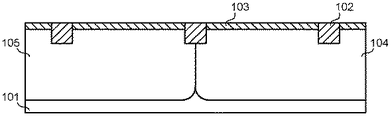
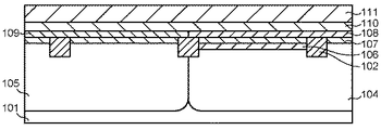
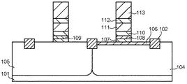
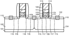
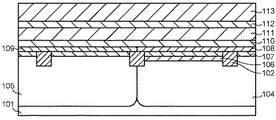
図1〜図8は、第1の実施形態における半導体装置の製造方法の一例における工程を示す断面図である。なお、本態様では、シングルメタルゲート型のトランジスタについて説明する。
図9及び図10は、第2の実施形態における半導体装置の製造方法の一例における工程を示す断面図である。なお、本態様でも、シングルメタルゲート型のトランジスタについて説明する。また、第1の実施形態と同一あるいは類似の構成要素に関しては、同一の参照数字を用いている。
上記第1の実施形態で得たトランジスタ構造に関して、RBS(ラザフォード後方散乱)測定を行った。結果を図11に示す。図11から明らかなように、GeがTiN膜111中に拡散しているとともに、TiN膜111及びHfSiON膜110の界面に偏析して、Ge介在物となっていることが分かる。
102 素子分離領域
103 犠牲酸化膜
104 N型拡散層
105 P型拡散層
106 SiGe層
107 ケミカルSiO2膜(シリコン酸化膜)
108 Al2O3膜
109 La2O3膜
110 HfSiON膜
111 TiN膜
112 Ge膜
113 多結晶シリコン膜
114 オフセットスペーサー
115 P型ソース・ドレイン拡散層
116 N型ソース・ドレイン拡散層
117 P型エクステンション拡散層
118 N型エクステンション拡散層
120 サイドウォールスペーサー
121 Ge介在物
122 シリサイド膜
123 2層のサイドウォールスペーサーを構成するSiO2膜
124 2層のサイドウォールスペーサーを構成するSiN膜
Claims (5)
- 素子分離膜によって分離されてなる、p型拡散層及びn型拡散層を有する半導体基板と、
前記半導体基板の、前記p型拡散層及びn型拡散層それぞれの上に形成されてなるゲート絶縁膜と、
前記ゲート絶縁膜上に形成された金属膜を含むゲート電極と、
前記ゲート絶縁膜と前記金属膜との界面に形成されたGe介在物と、
前記金属膜上に形成されたシリコン含有層と、
を具えることを特徴とする、半導体装置。 - 前記金属膜はGeを含むことを特徴とする、請求項1に記載の半導体装置。
- 前記金属膜は、窒化チタン、炭化タンタル、窒化タンタル、及び珪窒化タンタルからなる群より選ばれる少なくとも一種であることを特徴とする、請求項1又は2に記載の半導体装置。
- 半導体基板内に素子分離膜を形成するとともに、前記素子分離膜の一方の側にp型拡散層を形成し、前記素子分離膜の他方の側にn型拡散層を形成する工程と、
前記半導体基板の、前記p型拡散層及びn型拡散層それぞれの上にゲート絶縁膜を形成する工程と、
前記ゲート絶縁膜上に金属膜を含むゲート電極を形成する工程と、
前記金属膜上にGe層を形成するとともに熱処理を実施して、前記Ge層中のGeを前記ゲート絶縁膜と前記金属ゲート電極層との界面に拡散させて、Ge介在物を形成する工程と、
前記金属膜上にシリコン含有層を形成する工程と、
を具えることを特徴とする、半導体装置の製造方法。 - 半導体基板内に素子分離膜を形成するとともに、前記素子分離膜の一方の側にp型拡散層を形成し、前記素子分離膜の他方の側にn型拡散層を形成する工程と、
前記半導体基板の、前記p型拡散層及びn型拡散層それぞれの上にゲート絶縁膜を形成する工程と、
前記ゲート絶縁膜上に金属膜を含むゲート電極を形成する工程と、
前記金属ゲート電極上に多結晶シリコンを堆積する工程と、
前記多結晶シリコン層に対してGeイオン注入を行い、前記ゲート絶縁膜と前記金属膜との界面にGe介在物を形成する工程と、
前記金属膜上にシリコン含有層を形成する工程と、
を具えることを特徴とする、半導体装置の製造方法。
Priority Applications (2)
| Application Number | Priority Date | Filing Date | Title |
|---|---|---|---|
| JP2008239200A JP4837011B2 (ja) | 2008-09-18 | 2008-09-18 | 半導体装置、及び半導体装置の製造方法 |
| US12/561,862 US20100065918A1 (en) | 2008-09-18 | 2009-09-17 | Semiconductor device and method for manufacturing the same |
Applications Claiming Priority (1)
| Application Number | Priority Date | Filing Date | Title |
|---|---|---|---|
| JP2008239200A JP4837011B2 (ja) | 2008-09-18 | 2008-09-18 | 半導体装置、及び半導体装置の製造方法 |
Publications (2)
| Publication Number | Publication Date |
|---|---|
| JP2010073865A true JP2010073865A (ja) | 2010-04-02 |
| JP4837011B2 JP4837011B2 (ja) | 2011-12-14 |
Family
ID=42006444
Family Applications (1)
| Application Number | Title | Priority Date | Filing Date |
|---|---|---|---|
| JP2008239200A Expired - Fee Related JP4837011B2 (ja) | 2008-09-18 | 2008-09-18 | 半導体装置、及び半導体装置の製造方法 |
Country Status (2)
| Country | Link |
|---|---|
| US (1) | US20100065918A1 (ja) |
| JP (1) | JP4837011B2 (ja) |
Cited By (4)
| Publication number | Priority date | Publication date | Assignee | Title |
|---|---|---|---|---|
| JP2012015149A (ja) * | 2010-06-29 | 2012-01-19 | Tokyo Electron Ltd | エッチング方法及び装置 |
| JP2012146981A (ja) * | 2011-01-11 | 2012-08-02 | Imec | ゲルマニウム層の直接成長方法 |
| KR101212567B1 (ko) | 2010-12-22 | 2012-12-13 | 에스케이하이닉스 주식회사 | 반도체 장치 및 반도체 장치의 제조방법 |
| KR101282343B1 (ko) | 2010-07-30 | 2013-07-04 | 에스케이하이닉스 주식회사 | 금속게이트를 갖는 반도체장치 및 그 제조 방법 |
Families Citing this family (5)
| Publication number | Priority date | Publication date | Assignee | Title |
|---|---|---|---|---|
| US8350341B2 (en) * | 2010-04-09 | 2013-01-08 | International Business Machines Corporation | Method and structure for work function engineering in transistors including a high dielectric constant gate insulator and metal gate (HKMG) |
| JP5521726B2 (ja) * | 2010-04-16 | 2014-06-18 | 富士通セミコンダクター株式会社 | 半導体装置及びその製造方法 |
| US8941184B2 (en) | 2011-12-16 | 2015-01-27 | International Business Machines Corporation | Low threshold voltage CMOS device |
| KR102054834B1 (ko) | 2013-03-15 | 2019-12-12 | 삼성전자주식회사 | 반도체 메모리 소자 및 그 제조 방법 |
| US9418903B2 (en) * | 2014-05-21 | 2016-08-16 | Globalfoundries Inc. | Structure and method for effective device width adjustment in finFET devices using gate workfunction shift |
Citations (8)
| Publication number | Priority date | Publication date | Assignee | Title |
|---|---|---|---|---|
| JPH11251593A (ja) * | 1997-12-24 | 1999-09-17 | Texas Instr Inc <Ti> | ゲルマニウム層を使用した大誘電率ゲートの構造と方法 |
| JP2005191545A (ja) * | 2003-12-05 | 2005-07-14 | Toshiba Corp | 半導体装置 |
| JP2006261235A (ja) * | 2005-03-15 | 2006-09-28 | Toshiba Corp | 半導体装置 |
| JP2007013182A (ja) * | 2005-06-30 | 2007-01-18 | Samsung Electronics Co Ltd | Mosトランジスタを備える半導体素子及びその製造方法 |
| JP2007208260A (ja) * | 2006-01-31 | 2007-08-16 | Samsung Electronics Co Ltd | 二重仕事関数金属ゲートスタックを備えるcmos半導体装置 |
| JP2008016798A (ja) * | 2006-06-08 | 2008-01-24 | Toshiba Corp | 半導体装置およびその製造方法 |
| JP2008071814A (ja) * | 2006-09-12 | 2008-03-27 | Fujitsu Ltd | 半導体装置及びその製造方法 |
| JP2008135726A (ja) * | 2006-10-23 | 2008-06-12 | Interuniv Micro Electronica Centrum Vzw | 主電極を含むドープされた金属を含む半導体装置 |
Family Cites Families (3)
| Publication number | Priority date | Publication date | Assignee | Title |
|---|---|---|---|---|
| US6803611B2 (en) * | 2003-01-03 | 2004-10-12 | Texas Instruments Incorporated | Use of indium to define work function of p-type doped polysilicon |
| US7629212B2 (en) * | 2007-03-19 | 2009-12-08 | Texas Instruments Incorporated | Doped WGe to form dual metal gates |
| US7875520B2 (en) * | 2008-03-27 | 2011-01-25 | United Microelectronics Corp. | Method of forming CMOS transistor |
-
2008
- 2008-09-18 JP JP2008239200A patent/JP4837011B2/ja not_active Expired - Fee Related
-
2009
- 2009-09-17 US US12/561,862 patent/US20100065918A1/en not_active Abandoned
Patent Citations (8)
| Publication number | Priority date | Publication date | Assignee | Title |
|---|---|---|---|---|
| JPH11251593A (ja) * | 1997-12-24 | 1999-09-17 | Texas Instr Inc <Ti> | ゲルマニウム層を使用した大誘電率ゲートの構造と方法 |
| JP2005191545A (ja) * | 2003-12-05 | 2005-07-14 | Toshiba Corp | 半導体装置 |
| JP2006261235A (ja) * | 2005-03-15 | 2006-09-28 | Toshiba Corp | 半導体装置 |
| JP2007013182A (ja) * | 2005-06-30 | 2007-01-18 | Samsung Electronics Co Ltd | Mosトランジスタを備える半導体素子及びその製造方法 |
| JP2007208260A (ja) * | 2006-01-31 | 2007-08-16 | Samsung Electronics Co Ltd | 二重仕事関数金属ゲートスタックを備えるcmos半導体装置 |
| JP2008016798A (ja) * | 2006-06-08 | 2008-01-24 | Toshiba Corp | 半導体装置およびその製造方法 |
| JP2008071814A (ja) * | 2006-09-12 | 2008-03-27 | Fujitsu Ltd | 半導体装置及びその製造方法 |
| JP2008135726A (ja) * | 2006-10-23 | 2008-06-12 | Interuniv Micro Electronica Centrum Vzw | 主電極を含むドープされた金属を含む半導体装置 |
Cited By (5)
| Publication number | Priority date | Publication date | Assignee | Title |
|---|---|---|---|---|
| JP2012015149A (ja) * | 2010-06-29 | 2012-01-19 | Tokyo Electron Ltd | エッチング方法及び装置 |
| KR101282343B1 (ko) | 2010-07-30 | 2013-07-04 | 에스케이하이닉스 주식회사 | 금속게이트를 갖는 반도체장치 및 그 제조 방법 |
| US8653611B2 (en) | 2010-07-30 | 2014-02-18 | Hynix Semiconductor Inc. | Semiconductor device with metal gates and method for fabricating the same |
| KR101212567B1 (ko) | 2010-12-22 | 2012-12-13 | 에스케이하이닉스 주식회사 | 반도체 장치 및 반도체 장치의 제조방법 |
| JP2012146981A (ja) * | 2011-01-11 | 2012-08-02 | Imec | ゲルマニウム層の直接成長方法 |
Also Published As
| Publication number | Publication date |
|---|---|
| JP4837011B2 (ja) | 2011-12-14 |
| US20100065918A1 (en) | 2010-03-18 |
Similar Documents
| Publication | Publication Date | Title |
|---|---|---|
| JP4837011B2 (ja) | 半導体装置、及び半導体装置の製造方法 | |
| JP5442332B2 (ja) | 半導体装置およびその製造方法 | |
| US9287273B2 (en) | Method for manufacturing a semiconductor device comprising transistors each having a different effective work function | |
| US10424517B2 (en) | Method for manufacturing a dual work function semiconductor device and the semiconductor device made thereof | |
| JP4906868B2 (ja) | スペーサレスfet及びデュアル・ライナ法による歪み強化を増加させる構造体及び方法 | |
| US8119473B2 (en) | High temperature anneal for aluminum surface protection | |
| JP5336814B2 (ja) | 半導体装置およびその製造方法 | |
| JP2010161308A (ja) | 半導体装置およびその製造方法 | |
| JP5569173B2 (ja) | 半導体装置の製造方法及び半導体装置 | |
| US8198155B2 (en) | Semiconductor device and method of manufacturing the same | |
| JP2013506289A (ja) | 酸素拡散バリア層を有する半導体デバイスおよびそれを製造するための方法 | |
| JP2009111235A (ja) | 半導体装置およびその製造方法 | |
| US9196475B2 (en) | Methods for fabricating integrated circuits including fluorine incorporation | |
| JP2009194352A (ja) | 半導体装置の製造方法 | |
| JP2011187478A (ja) | 半導体装置およびその製造方法 | |
| TWI650798B (zh) | 半導體元件結構及其形成方法 | |
| WO2011057492A1 (zh) | 一种半导体器件及其制造方法 | |
| JP5203905B2 (ja) | 半導体装置およびその製造方法 | |
| JP2008277587A (ja) | 半導体装置及び半導体装置の製造方法 | |
| CN103178012A (zh) | 具有金属栅极的cmos器件及其形成方法 | |
| US20060267095A1 (en) | Semiconductor device | |
| JP2008218622A (ja) | 半導体装置およびその製造方法 | |
| JP2006059980A (ja) | 半導体装置及びその製造方法 | |
| JP2012054531A (ja) | 半導体装置及びその製造方法 | |
| JP2008117842A (ja) | 半導体装置、およびその製造方法 |
Legal Events
| Date | Code | Title | Description |
|---|---|---|---|
| A621 | Written request for application examination |
Free format text: JAPANESE INTERMEDIATE CODE: A621 Effective date: 20100804 |
|
| A977 | Report on retrieval |
Free format text: JAPANESE INTERMEDIATE CODE: A971007 Effective date: 20110117 |
|
| A131 | Notification of reasons for refusal |
Free format text: JAPANESE INTERMEDIATE CODE: A131 Effective date: 20110125 |
|
| A521 | Written amendment |
Free format text: JAPANESE INTERMEDIATE CODE: A523 Effective date: 20110325 |
|
| RD02 | Notification of acceptance of power of attorney |
Free format text: JAPANESE INTERMEDIATE CODE: A7422 Effective date: 20110325 |
|
| A131 | Notification of reasons for refusal |
Free format text: JAPANESE INTERMEDIATE CODE: A131 Effective date: 20110517 |
|
| A521 | Written amendment |
Free format text: JAPANESE INTERMEDIATE CODE: A523 Effective date: 20110715 |
|
| TRDD | Decision of grant or rejection written | ||
| A01 | Written decision to grant a patent or to grant a registration (utility model) |
Free format text: JAPANESE INTERMEDIATE CODE: A01 Effective date: 20110906 |
|
| A01 | Written decision to grant a patent or to grant a registration (utility model) |
Free format text: JAPANESE INTERMEDIATE CODE: A01 |
|
| A61 | First payment of annual fees (during grant procedure) |
Free format text: JAPANESE INTERMEDIATE CODE: A61 Effective date: 20110927 |
|
| FPAY | Renewal fee payment (event date is renewal date of database) |
Free format text: PAYMENT UNTIL: 20141007 Year of fee payment: 3 |
|
| FPAY | Renewal fee payment (event date is renewal date of database) |
Free format text: PAYMENT UNTIL: 20141007 Year of fee payment: 3 |
|
| LAPS | Cancellation because of no payment of annual fees |