JP2010061114A - 光走査装置及び画像形成装置 - Google Patents
光走査装置及び画像形成装置 Download PDFInfo
- Publication number
- JP2010061114A JP2010061114A JP2009163250A JP2009163250A JP2010061114A JP 2010061114 A JP2010061114 A JP 2010061114A JP 2009163250 A JP2009163250 A JP 2009163250A JP 2009163250 A JP2009163250 A JP 2009163250A JP 2010061114 A JP2010061114 A JP 2010061114A
- Authority
- JP
- Japan
- Prior art keywords
- optical
- light beam
- light
- polarization
- scanning device
- Prior art date
- Legal status (The legal status is an assumption and is not a legal conclusion. Google has not performed a legal analysis and makes no representation as to the accuracy of the status listed.)
- Granted
Links
Images


Classifications
-
- G—PHYSICS
- G02—OPTICS
- G02B—OPTICAL ELEMENTS, SYSTEMS OR APPARATUS
- G02B26/00—Optical devices or arrangements for the control of light using movable or deformable optical elements
- G02B26/08—Optical devices or arrangements for the control of light using movable or deformable optical elements for controlling the direction of light
- G02B26/10—Scanning systems
- G02B26/12—Scanning systems using multifaceted mirrors
- G02B26/123—Multibeam scanners, e.g. using multiple light sources or beam splitters
-
- G—PHYSICS
- G02—OPTICS
- G02B—OPTICAL ELEMENTS, SYSTEMS OR APPARATUS
- G02B26/00—Optical devices or arrangements for the control of light using movable or deformable optical elements
- G02B26/08—Optical devices or arrangements for the control of light using movable or deformable optical elements for controlling the direction of light
- G02B26/10—Scanning systems
- G02B26/12—Scanning systems using multifaceted mirrors
- G02B26/125—Details of the optical system between the polygonal mirror and the image plane
-
- G—PHYSICS
- G02—OPTICS
- G02B—OPTICAL ELEMENTS, SYSTEMS OR APPARATUS
- G02B27/00—Optical systems or apparatus not provided for by any of the groups G02B1/00 - G02B26/00, G02B30/00
- G02B27/28—Optical systems or apparatus not provided for by any of the groups G02B1/00 - G02B26/00, G02B30/00 for polarising
- G02B27/283—Optical systems or apparatus not provided for by any of the groups G02B1/00 - G02B26/00, G02B30/00 for polarising used for beam splitting or combining
-
- G—PHYSICS
- G03—PHOTOGRAPHY; CINEMATOGRAPHY; ANALOGOUS TECHNIQUES USING WAVES OTHER THAN OPTICAL WAVES; ELECTROGRAPHY; HOLOGRAPHY
- G03G—ELECTROGRAPHY; ELECTROPHOTOGRAPHY; MAGNETOGRAPHY
- G03G15/00—Apparatus for electrographic processes using a charge pattern
- G03G15/01—Apparatus for electrographic processes using a charge pattern for producing multicoloured copies
- G03G15/0105—Details of unit
- G03G15/011—Details of unit for exposing
-
- G—PHYSICS
- G03—PHOTOGRAPHY; CINEMATOGRAPHY; ANALOGOUS TECHNIQUES USING WAVES OTHER THAN OPTICAL WAVES; ELECTROGRAPHY; HOLOGRAPHY
- G03G—ELECTROGRAPHY; ELECTROPHOTOGRAPHY; MAGNETOGRAPHY
- G03G15/00—Apparatus for electrographic processes using a charge pattern
- G03G15/04—Apparatus for electrographic processes using a charge pattern for exposing, i.e. imagewise exposure by optically projecting the original image on a photoconductive recording material
- G03G15/04036—Details of illuminating systems, e.g. lamps, reflectors
-
- G—PHYSICS
- G03—PHOTOGRAPHY; CINEMATOGRAPHY; ANALOGOUS TECHNIQUES USING WAVES OTHER THAN OPTICAL WAVES; ELECTROGRAPHY; HOLOGRAPHY
- G03G—ELECTROGRAPHY; ELECTROPHOTOGRAPHY; MAGNETOGRAPHY
- G03G15/00—Apparatus for electrographic processes using a charge pattern
- G03G15/04—Apparatus for electrographic processes using a charge pattern for exposing, i.e. imagewise exposure by optically projecting the original image on a photoconductive recording material
- G03G15/043—Apparatus for electrographic processes using a charge pattern for exposing, i.e. imagewise exposure by optically projecting the original image on a photoconductive recording material with means for controlling illumination or exposure
- G03G15/0435—Apparatus for electrographic processes using a charge pattern for exposing, i.e. imagewise exposure by optically projecting the original image on a photoconductive recording material with means for controlling illumination or exposure by introducing an optical element in the optical path, e.g. a filter
-
- G—PHYSICS
- G03—PHOTOGRAPHY; CINEMATOGRAPHY; ANALOGOUS TECHNIQUES USING WAVES OTHER THAN OPTICAL WAVES; ELECTROGRAPHY; HOLOGRAPHY
- G03G—ELECTROGRAPHY; ELECTROPHOTOGRAPHY; MAGNETOGRAPHY
- G03G2215/00—Apparatus for electrophotographic processes
- G03G2215/04—Arrangements for exposing and producing an image
- G03G2215/0402—Exposure devices
- G03G2215/0404—Laser
Landscapes
- Physics & Mathematics (AREA)
- General Physics & Mathematics (AREA)
- Optics & Photonics (AREA)
- Facsimile Scanning Arrangements (AREA)
- Laser Beam Printer (AREA)
- Mechanical Optical Scanning Systems (AREA)
Abstract
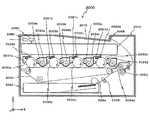
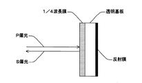
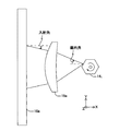
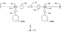
【解決手段】 fθレンズ15aを介したP偏光は、偏光ビームスプリッタ16aを透過し、1/4波長板17aと反射ミラー18aとによってS偏光に変換された後、偏光ビームスプリッタ16aに再度入射し、偏光ビームスプリッタ16aで−Z方向に反射される。そして、ポリゴンミラー141からfθレンズ15aに向かう光束の光路と、fθレンズ15aから偏光ビームスプリッタ16aに向かう光束の光路と、偏光ビームスプリッタ16aから1/4波長板17aに向かう光束の光路と、1/4波長板17aから反射ミラー18aに向かう光束の光路と、反射ミラー18aから1/4波長板17aに向かう光束の光路と、1/4波長板17aから偏光ビームスプリッタ16aに向かう光束の光路は、同一の面内に存在している。
【選択図】図4
Description

Claims (17)
- 光束により被走査面を走査する光走査装置であって、
光源ユニットと;
前記光源ユニットからの光束を偏向する偏向器と:
前記偏向器で偏向された光束を前記被走査面上に集光する走査光学系と;を備え、
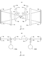
前記走査光学系は、偏光分離素子と反射型光学素子と変換光学系とを含み、
前記偏光分離素子は、前記偏向器からの第1の偏光状態の光束を透過させ、
前記変換光学系は、前記偏光分離素子を透過した前記第1の偏光状態の光束の光路上に配置され、前記偏光分離素子を透過した前記第1の偏光状態の光束の偏光状態を第2の偏光状態に変換し、
前記反射型光学素子は、前記変換光学系で変換された前記第2の偏光状態の光束が入射され、該光束の偏光状態を前記第2の偏光状態から第3の偏光状態に変換して、前記変換光学系に向けて反射し、
前記変換光学系は、前記反射型光学素子にて反射された前記第3の偏光状態の光束を第4の状態に変換して、前記偏光分離素子に向けて射出し、
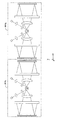
前記偏光分離素子は、前記変換光学系からの前記第4の偏光状態の光束の光路を前記被走査面に向かう方向に折り返すことを特徴とする光走査装置。 - 前記偏光分離素子から前記反射型光学素子に向かう光束の光路、及び前記反射型光学素子から前記偏光分離素子に向かう光束の光路は、いずれも同一面内にあることを特徴とする請求項1に記載の光走査装置。
- 前記偏光分離素子から前記反射型光学素子に向かう光束の光路、及び前記反射型光学素子から前記偏光分離素子に向かう光束の光路は、いずれも前記偏向器の偏向反射面で偏向された光束が経時的に形成する光線束面である偏向面が含まれる面内にあることを特徴とする請求項2に記載の光走査装置。
- 前記変換光学系は、反射型光学素子、及び該反射型光学素子と前記偏光分離素子との間の光路上に配置され、入射光の波長λ、0以上の整数mを用いて、{(m/2)±1/4}λの光学的位相差を入射光に付与する位相差板を有することを特徴とする請求項1〜3のいずれか一項に記載の光走査装置。
- 前記偏光分離素子から前記位相差板に向かう光束の光路、前記位相差板から前記反射型光学素子に向かう光束の光路、前記反射型光学素子から前記位相差板に向かう光束の光路、及び前記位相差板から前記偏光分離素子に向かう光束の光路は、いずれも同一面内にあることを特徴とする請求項4に記載の光走査装置。
- 前記偏光分離素子から前記位相差板に向かう光束の光路、前記位相差板から前記反射型光学素子に向かう光束の光路、前記反射型光学素子から前記位相差板に向かう光束の光路、及び前記位相差板から前記偏光分離素子に向かう光束の光路は、いずれも前記偏向器の偏向反射面で偏向された光束が経時的に形成する光線束面である偏向面が含まれる面内にあることを特徴とする請求項5に記載の光走査装置。
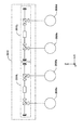
- 前記走査光学系は透過型結像光学素子を有し、
前記透過型結像光学素子は、前記偏光分離素子と前記反射型光学素子との間の光路上に配置され、
前記偏光分離素子から前記反射型光学素子に向かう光束、及び前記反射型光学素子から前記偏光分離素子に向かう光束は、いずれも前記透過型結像光学素子を通過することを特徴とする請求項1〜6のいずれか一項に記載の光走査装置。 - 前記反射光学素子は、平面ミラーであることを特徴とする請求項7に記載の光走査装置。
- 前記変換光学系は、更に前記偏光分離素子に向けて出力する光束を収束光とすることを特徴とする請求項1〜3のいずれか一項に記載の光走査装置。
- 前記変換光学系は、入射する光束に対して、集光機能及び等速走査機能を有することを特徴とする請求項9に記載の光走査装置。
- 前記偏光分離素子は、偏光ビームスプリッタであることを特徴とする請求項1〜10のいずれか一項に記載の光走査装置。
- 前記光源ユニットは、前記偏向器での偏向角に応じて、光出力の大きさを調整することを特徴とする請求項1〜11のいずれか一項に記載の光走査装置。
- 前記光源ユニットは、前記第1の偏光方向の光束を出力することを特徴とする請求項1〜12のいずれか一項に記載の光走査装置。
- 前記光源ユニットは、垂直共振器型の面発光レーザを含むことを特徴とする請求項1〜13のいずれか一項に記載の光走査装置。
- 前記光源ユニットは、複数の発光部を有することを特徴とする請求項1〜14のいずれか一項に記載の光走査装置。
- 少なくとも1つの像担持体と;
前記少なくとも1つの像担持体を画像情報が含まれる光束により走査する少なくとも1つの請求項1〜15のいずれか一項に記載の光走査装置と;を備える画像形成装置。 - 前記画像情報は、多色の画像情報であることを特徴とする請求項16に記載の画像形成装置。
Priority Applications (2)
| Application Number | Priority Date | Filing Date | Title |
|---|---|---|---|
| JP2009163250A JP5288333B2 (ja) | 2008-08-06 | 2009-07-10 | 光走査装置及び画像形成装置 |
| US12/534,896 US8373736B2 (en) | 2008-08-06 | 2009-08-04 | Optical scanning device and image forming apparatus |
Applications Claiming Priority (3)
| Application Number | Priority Date | Filing Date | Title |
|---|---|---|---|
| JP2008202498 | 2008-08-06 | ||
| JP2008202498 | 2008-08-06 | ||
| JP2009163250A JP5288333B2 (ja) | 2008-08-06 | 2009-07-10 | 光走査装置及び画像形成装置 |
Publications (2)
| Publication Number | Publication Date |
|---|---|
| JP2010061114A true JP2010061114A (ja) | 2010-03-18 |
| JP5288333B2 JP5288333B2 (ja) | 2013-09-11 |
Family
ID=41653080
Family Applications (1)
| Application Number | Title | Priority Date | Filing Date |
|---|---|---|---|
| JP2009163250A Expired - Fee Related JP5288333B2 (ja) | 2008-08-06 | 2009-07-10 | 光走査装置及び画像形成装置 |
Country Status (2)
| Country | Link |
|---|---|
| US (1) | US8373736B2 (ja) |
| JP (1) | JP5288333B2 (ja) |
Cited By (4)
| Publication number | Priority date | Publication date | Assignee | Title |
|---|---|---|---|---|
| JP2011221493A (ja) * | 2010-03-24 | 2011-11-04 | Ricoh Co Ltd | 光走査装置及び画像形成装置 |
| JP2012047863A (ja) * | 2010-08-25 | 2012-03-08 | Ricoh Co Ltd | 光走査装置及び画像形成装置 |
| JP2012048092A (ja) * | 2010-08-30 | 2012-03-08 | Ricoh Co Ltd | 光学素子、光走査装置及び画像形成装置 |
| WO2014045555A1 (ja) * | 2012-09-19 | 2014-03-27 | 日本電気株式会社 | 光走査器およびそれを用いた画像表示装置 |
Families Citing this family (2)
| Publication number | Priority date | Publication date | Assignee | Title |
|---|---|---|---|---|
| JP5885060B2 (ja) * | 2010-10-06 | 2016-03-15 | 株式会社リコー | 光走査装置および画像形成装置 |
| JP6489410B2 (ja) | 2014-03-17 | 2019-03-27 | 株式会社リコー | 光走査装置および画像形成装置 |
Citations (3)
| Publication number | Priority date | Publication date | Assignee | Title |
|---|---|---|---|---|
| JPH04110818A (ja) * | 1990-08-30 | 1992-04-13 | Minolta Camera Co Ltd | 光ビーム走査光学系 |
| JPH04168411A (ja) * | 1990-10-31 | 1992-06-16 | Dainippon Screen Mfg Co Ltd | 光偏向器 |
| JPH10206781A (ja) * | 1997-01-17 | 1998-08-07 | Fuji Photo Film Co Ltd | 光走査光学系 |
Family Cites Families (31)
| Publication number | Priority date | Publication date | Assignee | Title |
|---|---|---|---|---|
| US5119452A (en) | 1989-06-13 | 1992-06-02 | Ricoh Company, Ltd. | High efficiency prism coupling device and method for producing the same |
| US5124835A (en) | 1989-06-21 | 1992-06-23 | Ricoh Company, Ltd. | Optical scanning apparatus |
| US5031978A (en) | 1989-08-18 | 1991-07-16 | Ricoh Company, Ltd. | Recording optical system |
| US5175642A (en) | 1989-12-27 | 1992-12-29 | Ricoh Company, Ltd. | Light source unit capable of changing size of light beam spot and optical scanning image recording apparatus using the same |
| JPH03214944A (ja) | 1990-01-19 | 1991-09-20 | Matsushita Electric Ind Co Ltd | サイクリック伝送型自己診断装置 |
| JPH04219657A (ja) | 1990-04-13 | 1992-08-10 | Ricoh Co Ltd | 光磁気情報記録再生装置及びモードスプリッタ |
| US5233457A (en) * | 1990-08-30 | 1993-08-03 | Minolta Camera Kabushiki Kaisha | Beam scanning optical system |
| EP0483827B1 (en) * | 1990-10-31 | 1997-01-02 | Dainippon Screen Mfg. Co., Ltd. | Apparatus for scanning drum inner face and method of scanning therefor |
| US5426298A (en) | 1992-03-17 | 1995-06-20 | Ricoh Company, Ltd. | Optical scanner |
| JP3214944B2 (ja) | 1992-03-17 | 2001-10-02 | 株式会社リコー | 光走査装置 |
| JPH0659210A (ja) * | 1992-08-11 | 1994-03-04 | Minolta Camera Co Ltd | 画像書き込み装置 |
| JP2698521B2 (ja) * | 1992-12-14 | 1998-01-19 | キヤノン株式会社 | 反射屈折型光学系及び該光学系を備える投影露光装置 |
| JPH07113970A (ja) | 1993-10-15 | 1995-05-02 | Konica Corp | 走査光学系装置 |
| JPH103048A (ja) | 1996-06-14 | 1998-01-06 | Ricoh Co Ltd | 多色画像形成装置の光走査装置 |
| US6072579A (en) | 1998-08-27 | 2000-06-06 | Ricoh Company, Ltd. | Optical pickup apparatus having improved holographic optical element and photodetector |
| JP2000330052A (ja) * | 1999-05-20 | 2000-11-30 | Fuji Photo Film Co Ltd | 内面走査型画像記録装置 |
| JP2001117041A (ja) | 1999-10-19 | 2001-04-27 | Ricoh Co Ltd | 光走査装置及び画像形成装置 |
| JP3804928B2 (ja) | 2001-03-09 | 2006-08-02 | 株式会社リコー | 液体噴射記録装置 |
| JP4676662B2 (ja) | 2001-09-21 | 2011-04-27 | 株式会社リコー | カラー画像形成装置 |
| KR100452852B1 (ko) * | 2002-01-09 | 2004-10-14 | 삼성전자주식회사 | 확대 광학계 및 그것을 갖는 화상형성 장치 |
| JP2004074643A (ja) | 2002-08-20 | 2004-03-11 | Ricoh Co Ltd | 色ずれ補正方法、光書き込み装置及び画像形成装置 |
| JP2005011478A (ja) | 2003-04-24 | 2005-01-13 | Ricoh Co Ltd | 回折格子とその作製方法及び複製方法並びにその回折格子を用いた光ヘッド装置及び光ディスクドライブ装置 |
| JP2005148128A (ja) | 2003-11-11 | 2005-06-09 | Ricoh Co Ltd | 光書込装置及び画像形成装置 |
| JP4480075B2 (ja) | 2004-09-16 | 2010-06-16 | 株式会社リコー | 光書き込み装置及び画像形成装置 |
| JP4786261B2 (ja) | 2005-09-06 | 2011-10-05 | 株式会社リコー | 光走査装置及び画像形成装置 |
| JP4694926B2 (ja) | 2005-09-16 | 2011-06-08 | 株式会社リコー | 光走査装置及び画像形成装置 |
| US7916161B2 (en) | 2006-02-13 | 2011-03-29 | Ricoh Company, Ltd. | Image forming apparatus |
| JP2007225680A (ja) | 2006-02-21 | 2007-09-06 | Canon Inc | 走査光学装置およびカラー画像形成装置 |
| JP2008033141A (ja) | 2006-07-31 | 2008-02-14 | Ricoh Co Ltd | 光走査装置および光走査装置を用いた画像形成装置 |
| JP4918439B2 (ja) | 2007-09-04 | 2012-04-18 | 株式会社リコー | 光書込装置及び画像形成装置 |
| JP5033548B2 (ja) | 2007-09-10 | 2012-09-26 | 株式会社リコー | 光書込装置及び画像形成装置 |
-
2009
- 2009-07-10 JP JP2009163250A patent/JP5288333B2/ja not_active Expired - Fee Related
- 2009-08-04 US US12/534,896 patent/US8373736B2/en not_active Expired - Fee Related
Patent Citations (3)
| Publication number | Priority date | Publication date | Assignee | Title |
|---|---|---|---|---|
| JPH04110818A (ja) * | 1990-08-30 | 1992-04-13 | Minolta Camera Co Ltd | 光ビーム走査光学系 |
| JPH04168411A (ja) * | 1990-10-31 | 1992-06-16 | Dainippon Screen Mfg Co Ltd | 光偏向器 |
| JPH10206781A (ja) * | 1997-01-17 | 1998-08-07 | Fuji Photo Film Co Ltd | 光走査光学系 |
Cited By (5)
| Publication number | Priority date | Publication date | Assignee | Title |
|---|---|---|---|---|
| JP2011221493A (ja) * | 2010-03-24 | 2011-11-04 | Ricoh Co Ltd | 光走査装置及び画像形成装置 |
| JP2012047863A (ja) * | 2010-08-25 | 2012-03-08 | Ricoh Co Ltd | 光走査装置及び画像形成装置 |
| US8913096B2 (en) | 2010-08-25 | 2014-12-16 | Ricoh Company, Limited | Optical scanning device and image forming apparatus |
| JP2012048092A (ja) * | 2010-08-30 | 2012-03-08 | Ricoh Co Ltd | 光学素子、光走査装置及び画像形成装置 |
| WO2014045555A1 (ja) * | 2012-09-19 | 2014-03-27 | 日本電気株式会社 | 光走査器およびそれを用いた画像表示装置 |
Also Published As
| Publication number | Publication date |
|---|---|
| US8373736B2 (en) | 2013-02-12 |
| US20100034563A1 (en) | 2010-02-11 |
| JP5288333B2 (ja) | 2013-09-11 |
Similar Documents
| Publication | Publication Date | Title |
|---|---|---|
| JP5381371B2 (ja) | 偏光分離デバイス、光走査装置及び画像形成装置 | |
| JP5034053B2 (ja) | 光走査装置および画像形成装置 | |
| JP5033548B2 (ja) | 光書込装置及び画像形成装置 | |
| US8848013B2 (en) | Optical scanning device and image forming apparatus including a plurality of scanned members | |
| JP4918439B2 (ja) | 光書込装置及び画像形成装置 | |
| JP5464354B2 (ja) | 光走査装置及び該光走査装置を備える画像形成装置 | |
| JP5278253B2 (ja) | 光走査装置及び画像形成装置 | |
| TW200306256A (en) | Color laser printer | |
| JP5288333B2 (ja) | 光走査装置及び画像形成装置 | |
| JP2011191370A (ja) | 光走査装置及び画像形成装置 | |
| JP2013068694A (ja) | 光走査装置及び画像形成装置 | |
| JP5754617B2 (ja) | 光走査装置及び画像形成装置 | |
| JP5017030B2 (ja) | 光書込装置及び画像形成装置 | |
| JP2012233931A (ja) | 光走査装置及び画像形成装置 | |
| JP5440911B2 (ja) | 偏光分離デバイス、光走査装置及び画像形成装置 | |
| JP2011085776A (ja) | 偏光分離デバイス、光走査装置及び画像形成装置 | |
| JP5871119B2 (ja) | 光走査装置及び画像形成装置 | |
| JP2012013731A (ja) | 光走査装置及び画像形成装置 | |
| JP5022945B2 (ja) | 光書込装置及び画像形成装置 | |
| JP2010160295A (ja) | 偏光分離デバイス、光走査装置及び画像形成装置 | |
| JP5971452B2 (ja) | 光走査装置及び画像形成装置 | |
| JP5251571B2 (ja) | 光走査装置、および画像形成装置 | |
| JP2012163868A (ja) | 光走査装置及び画像形成装置 | |
| JP5322022B2 (ja) | 光走査装置、画像形成装置及びレーザ描画装置 | |
| JP5846427B2 (ja) | 光走査装置及び画像形成装置 |
Legal Events
| Date | Code | Title | Description |
|---|---|---|---|
| A621 | Written request for application examination |
Free format text: JAPANESE INTERMEDIATE CODE: A621 Effective date: 20120528 |
|
| A977 | Report on retrieval |
Free format text: JAPANESE INTERMEDIATE CODE: A971007 Effective date: 20130129 |
|
| A131 | Notification of reasons for refusal |
Free format text: JAPANESE INTERMEDIATE CODE: A131 Effective date: 20130204 |
|
| A521 | Written amendment |
Free format text: JAPANESE INTERMEDIATE CODE: A523 Effective date: 20130402 |
|
| TRDD | Decision of grant or rejection written | ||
| A01 | Written decision to grant a patent or to grant a registration (utility model) |
Free format text: JAPANESE INTERMEDIATE CODE: A01 Effective date: 20130513 |
|
| R151 | Written notification of patent or utility model registration |
Ref document number: 5288333 Country of ref document: JP Free format text: JAPANESE INTERMEDIATE CODE: R151 |
|
| A61 | First payment of annual fees (during grant procedure) |
Free format text: JAPANESE INTERMEDIATE CODE: A61 Effective date: 20130526 |
|
| LAPS | Cancellation because of no payment of annual fees |