JP2010045362A - ウェーハおよびウェーハの製造方法 - Google Patents
ウェーハおよびウェーハの製造方法 Download PDFInfo
- Publication number
- JP2010045362A JP2010045362A JP2009186536A JP2009186536A JP2010045362A JP 2010045362 A JP2010045362 A JP 2010045362A JP 2009186536 A JP2009186536 A JP 2009186536A JP 2009186536 A JP2009186536 A JP 2009186536A JP 2010045362 A JP2010045362 A JP 2010045362A
- Authority
- JP
- Japan
- Prior art keywords
- substrate
- layer
- wafer
- grown
- growth
- Prior art date
- Legal status (The legal status is an assumption and is not a legal conclusion. Google has not performed a legal analysis and makes no representation as to the accuracy of the status listed.)
- Granted
Links
Images


Classifications
-
- H10P14/20—
-
- H10P90/12—
-
- C—CHEMISTRY; METALLURGY
- C30—CRYSTAL GROWTH
- C30B—SINGLE-CRYSTAL GROWTH; UNIDIRECTIONAL SOLIDIFICATION OF EUTECTIC MATERIAL OR UNIDIRECTIONAL DEMIXING OF EUTECTOID MATERIAL; REFINING BY ZONE-MELTING OF MATERIAL; PRODUCTION OF A HOMOGENEOUS POLYCRYSTALLINE MATERIAL WITH DEFINED STRUCTURE; SINGLE CRYSTALS OR HOMOGENEOUS POLYCRYSTALLINE MATERIAL WITH DEFINED STRUCTURE; AFTER-TREATMENT OF SINGLE CRYSTALS OR A HOMOGENEOUS POLYCRYSTALLINE MATERIAL WITH DEFINED STRUCTURE; APPARATUS THEREFOR
- C30B25/00—Single-crystal growth by chemical reaction of reactive gases, e.g. chemical vapour-deposition growth
- C30B25/02—Epitaxial-layer growth
- C30B25/18—Epitaxial-layer growth characterised by the substrate
- C30B25/183—Epitaxial-layer growth characterised by the substrate being provided with a buffer layer, e.g. a lattice matching layer
Landscapes
- Chemical & Material Sciences (AREA)
- Chemical Kinetics & Catalysis (AREA)
- General Chemical & Material Sciences (AREA)
- Engineering & Computer Science (AREA)
- Crystallography & Structural Chemistry (AREA)
- Materials Engineering (AREA)
- Metallurgy (AREA)
- Organic Chemistry (AREA)
- Recrystallisation Techniques (AREA)
- Mechanical Treatment Of Semiconductor (AREA)
Abstract
【解決手段】単結晶の第1の材料の基板はオンアクシスシリコン基板であり、オンアクシスシリコン基板上に第2の材料を成長させるウェーハの製造方法に関し、第2の材料が、第1の材料上にエピタキシャル成長し、第1の材料の格子とは異なる格子を持っている。オンアクシスシリコン基板を研磨ステップ104で研磨して、ウェーハ表面粗さを増大させる。SiGe層である傾斜バッファ層及び緩和層をウェーハ上に形成した後、CMP最終研磨108を実施する。上述のタイプの方法により解決され、基板の最終表面仕上げの前に第2の材料の成長を実施する。
【選択図】図1
Description
本発明の好ましい例では、約0.15ナノメートルRMS〜約0.4ナノメートルRMSの表面粗さの基板上に、第2の材料が成長する。この範囲の表面粗さが第1の材料上への第2の材料の小さい応力での成長に特に効果的である。
本発明の有益な実施形態では、平方ミリメートル当たり0.12マイクロメートルより大きいサイズの欠陥が約0.2個〜約1個の表面欠陥密度の基板上に、第2の材料が成長する。意外にも、欠陥は第2の材料のよりよい開始層の確立に有益である。
Claims (11)
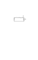
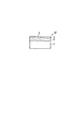
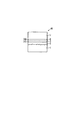
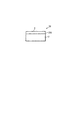
- 単結晶の第1の材料の基板(1)と、前記第1の材料上にエピタキシャル成長し、前記第1の材料の格子とは異なる格子を持った第2の材料の少なくとも1つの層(2、3)と、を具備したウェーハ(52、62)の製造方法において、
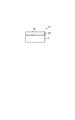
スライスされラッピングされ及び/又は研削されただけの準備の整っていない基板の表面に実施されるエッチングステップ(103)であって、軽減されたアルカリ性によるエッチングを含み、エッチングされた基板(1)の表面がより損傷を受けた状態とするエッチングステップと、1平方マイクロメートルのスキャンにつき0.2ナノメートルRMS未満の表面粗さを有する少なくとも1つのヘテロエピタキシャル層(2,3)の仕上げられた表面を形成する最終研磨ステップ(108)との間に、前記第2の材料の成長を実施することを特徴とする方法。 - 前記第2の材料の成長は、傾斜バッファ層(2)およびその上に形成される緩和層(3)の成長を含むことを特徴とする請求項1に記載の方法。
- 前記傾斜バッファ層(2)の成長は傾斜SiGe層の成長を含み、そのゲルマニウム含有量は前記基板(1)から始まって徐々に増大することを特徴とする請求項2に記載の方法。
- 緩和層(3)の材料厚さは、前記最終研磨ステップ(108)を実施する前に適用されるCMPストック除去ステップ(107)により除去されることを特徴とする請求項2または3に記載の方法。
- 単結晶の第1の材料の基板はオンアクシスシリコン基板であり、当該オンアクシスシリコン基板上に前記第2の材料を成長させることを特徴とする請求項1〜4のいずれか1項に記載の方法。
- 平方ミリメートル当たり0.12マイクロメートルより大きいサイズの欠陥が0.2個〜1個の表面欠陥密度の基板(1)上に、前記第2の材料を成長させる
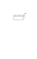
ことを特徴とする請求項1に記載の方法。 - 単結晶の第1の材料の基板(1)と、前記第1の材料上にエピタキシャル成長し、前記第1の材料の格子とは異なる格子を持った第2の材料の少なくとも1つの層(2、3)と、を具備したウェーハ(52、62)において、
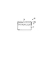
前記第2の材料の前記少なくとも1つの層(2、3)が成長する前記基板(1)の表面は、スライスされラッピングされ及び/又は研削されただけの準備の整っていない基板の表面で、且つ、0.15ナノメートルRMS〜0.4ナノメートルRMSの表面粗さを有する表面であり、へテロエピタキシャル層である前記少なくとも1つの層(2、3)の表面(8)は研磨され、1平方マイクロメートルのスキャンにつき0.2ナノメートルRMS未満の表面粗さを有することを特徴とするウェーハ。 - 前記少なくとも1つのヘテロエピタキシャル層(2、3)は、傾斜バッファ層(2)およびその上に形成された緩和層(3)を備えることを特徴とする請求項7に記載のウェーハ。
- 前記傾斜バッファ層(2)は傾斜SiGe層を備え、そのゲルマニウム含有量は前記基板(1)から始まって徐々に増大することを特徴とする請求項8に記載のウェーハ。
- 前記第1の材料はシリコンまたはゲルマニウムであり、前記第2の材料はSiGe、AsGa、GaNまたはゲルマニウムであることを特徴とする請求項7に記載のウェーハ。
- 前記第1の材料はシリコンまたはゲルマニウムであり、前記第2の材料はSiGe、AsGa、GaNまたはゲルマニウムであることを特徴とする請求項1に記載のウェーハの製造方法。
Applications Claiming Priority (2)
| Application Number | Priority Date | Filing Date | Title |
|---|---|---|---|
| EP04291473.9 | 2004-06-11 | ||
| EP04291473A EP1605498A1 (en) | 2004-06-11 | 2004-06-11 | A method of manufacturing a semiconductor wafer |
Related Parent Applications (1)
| Application Number | Title | Priority Date | Filing Date |
|---|---|---|---|
| JP2005172558A Division JP2006054428A (ja) | 2004-06-11 | 2005-06-13 | ウェーハの製造方法 |
Publications (2)
| Publication Number | Publication Date |
|---|---|
| JP2010045362A true JP2010045362A (ja) | 2010-02-25 |
| JP5005740B2 JP5005740B2 (ja) | 2012-08-22 |
Family
ID=34931173
Family Applications (2)
| Application Number | Title | Priority Date | Filing Date |
|---|---|---|---|
| JP2005172558A Withdrawn JP2006054428A (ja) | 2004-06-11 | 2005-06-13 | ウェーハの製造方法 |
| JP2009186536A Expired - Lifetime JP5005740B2 (ja) | 2004-06-11 | 2009-08-11 | ウェーハおよびウェーハの製造方法 |
Family Applications Before (1)
| Application Number | Title | Priority Date | Filing Date |
|---|---|---|---|
| JP2005172558A Withdrawn JP2006054428A (ja) | 2004-06-11 | 2005-06-13 | ウェーハの製造方法 |
Country Status (5)
| Country | Link |
|---|---|
| US (1) | US7138325B2 (ja) |
| EP (1) | EP1605498A1 (ja) |
| JP (2) | JP2006054428A (ja) |
| KR (1) | KR100712042B1 (ja) |
| CN (1) | CN100413028C (ja) |
Families Citing this family (22)
| Publication number | Priority date | Publication date | Assignee | Title |
|---|---|---|---|---|
| US7175709B2 (en) * | 2004-05-17 | 2007-02-13 | Taiwan Semiconductor Manufacturing Co., Ltd. | Epitaxy layer and method of forming the same |
| US9685524B2 (en) | 2005-03-11 | 2017-06-20 | Vishay-Siliconix | Narrow semiconductor trench structure |
| TWI489557B (zh) | 2005-12-22 | 2015-06-21 | 維雪 希里康尼克斯公司 | 高移動率p-通道溝槽及平面型空乏模式的功率型金屬氧化物半導體場效電晶體 |
| US8409954B2 (en) | 2006-03-21 | 2013-04-02 | Vishay-Silconix | Ultra-low drain-source resistance power MOSFET |
| US8361337B2 (en) * | 2007-03-19 | 2013-01-29 | The University Of Massachusetts | Method of producing nanopatterned templates |
| US8981427B2 (en) * | 2008-07-15 | 2015-03-17 | Taiwan Semiconductor Manufacturing Company, Ltd. | Polishing of small composite semiconductor materials |
| US8247033B2 (en) | 2008-09-19 | 2012-08-21 | The University Of Massachusetts | Self-assembly of block copolymers on topographically patterned polymeric substrates |
| US8211737B2 (en) | 2008-09-19 | 2012-07-03 | The University Of Massachusetts | Method of producing nanopatterned articles, and articles produced thereby |
| US8518837B2 (en) | 2008-09-25 | 2013-08-27 | The University Of Massachusetts | Method of producing nanopatterned articles using surface-reconstructed block copolymer films |
| US7927975B2 (en) | 2009-02-04 | 2011-04-19 | Micron Technology, Inc. | Semiconductor material manufacture |
| WO2010119833A1 (ja) * | 2009-04-13 | 2010-10-21 | 株式会社Sumco | シリコンエピタキシャルウェーハの製造方法 |
| JP5381304B2 (ja) * | 2009-05-08 | 2014-01-08 | 株式会社Sumco | シリコンエピタキシャルウェーハの製造方法 |
| US9012253B2 (en) * | 2009-12-16 | 2015-04-21 | Micron Technology, Inc. | Gallium nitride wafer substrate for solid state lighting devices, and associated systems and methods |
| US9455146B2 (en) * | 2009-12-17 | 2016-09-27 | California Institute Of Technology | Virtual substrates for epitaxial growth and methods of making the same |
| TWI510682B (zh) * | 2011-01-28 | 2015-12-01 | Sino American Silicon Prod Inc | 晶棒表面奈米化製程、晶圓製造方法及其晶圓 |
| US9156682B2 (en) | 2011-05-25 | 2015-10-13 | The University Of Massachusetts | Method of forming oriented block copolymer line patterns, block copolymer line patterns formed thereby, and their use to form patterned articles |
| US8492187B2 (en) | 2011-09-29 | 2013-07-23 | International Business Machines Corporation | High throughput epitaxial liftoff for releasing multiple semiconductor device layers from a single base substrate |
| US9412883B2 (en) | 2011-11-22 | 2016-08-09 | Taiwan Semiconductor Manufacturing Company, Ltd. | Methods and apparatus for MOS capacitors in replacement gate process |
| DE102018221922A1 (de) * | 2018-12-17 | 2020-06-18 | Siltronic Ag | Verfahren zur Herstellung von Halbleiterscheiben mittels einer Drahtsäge, Drahtsäge und Halbleiterscheibe aus einkristallinem Silizium |
| US11515408B2 (en) * | 2020-03-02 | 2022-11-29 | Taiwan Semiconductor Manufacturing Company, Ltd. | Rough buffer layer for group III-V devices on silicon |
| US11555250B2 (en) * | 2020-04-29 | 2023-01-17 | Applied Materials, Inc. | Organic contamination free surface machining |
| JP7487655B2 (ja) * | 2020-12-23 | 2024-05-21 | 株式会社Sumco | シリコンウェーハの抵抗率測定方法 |
Citations (12)
| Publication number | Priority date | Publication date | Assignee | Title |
|---|---|---|---|---|
| JPS5051668A (ja) * | 1973-08-21 | 1975-05-08 | ||
| JPH10172976A (ja) * | 1996-12-12 | 1998-06-26 | Mitsubishi Materials Shilicon Corp | Eg層付きエピタキシャルウェーハの製造方法 |
| JPH11135792A (ja) * | 1997-10-27 | 1999-05-21 | Sony Corp | 半導体装置の製造方法 |
| JP2000243699A (ja) * | 1999-02-23 | 2000-09-08 | Hitachi Ltd | 半導体ウェハの製造方法および半導体装置の製造方法 |
| JP2001223163A (ja) * | 2000-02-09 | 2001-08-17 | Shin Etsu Handotai Co Ltd | シリコンエピタキシャルウェーハ及びその製造方法 |
| JP2001257243A (ja) * | 2000-03-09 | 2001-09-21 | Mitsubishi Materials Silicon Corp | シリコンウェーハ表面上の微粒子の測定方法 |
| JP2002289611A (ja) * | 2001-03-26 | 2002-10-04 | Toshiba Corp | 半導体装置の製造方法及び製造装置 |
| JP2003142686A (ja) * | 2001-11-07 | 2003-05-16 | Sumitomo Mitsubishi Silicon Corp | 半導体基板の製造方法及び電界効果型トランジスタの製造方法並びに半導体基板及び電界効果型トランジスタ |
| JP2003158075A (ja) * | 2001-08-23 | 2003-05-30 | Sumitomo Mitsubishi Silicon Corp | 半導体基板の製造方法及び電界効果型トランジスタの製造方法並びに半導体基板及び電界効果型トランジスタ |
| JP2003243404A (ja) * | 2002-02-21 | 2003-08-29 | Shin Etsu Handotai Co Ltd | アニールウエーハの製造方法及びアニールウエーハ |
| JP2003347399A (ja) * | 2002-05-23 | 2003-12-05 | Sharp Corp | 半導体基板の製造方法 |
| JP2004342818A (ja) * | 2003-05-15 | 2004-12-02 | Toshiba Ceramics Co Ltd | 半導体基板の製造方法 |
Family Cites Families (11)
| Publication number | Priority date | Publication date | Assignee | Title |
|---|---|---|---|---|
| TW230822B (ja) * | 1993-03-02 | 1994-09-21 | Sumitomo Electric Industries | |
| JP3120825B2 (ja) * | 1994-11-14 | 2000-12-25 | 信越半導体株式会社 | エピタキシャルウエーハ及びその製造方法 |
| US6039803A (en) * | 1996-06-28 | 2000-03-21 | Massachusetts Institute Of Technology | Utilization of miscut substrates to improve relaxed graded silicon-germanium and germanium layers on silicon |
| US6174727B1 (en) * | 1998-11-03 | 2001-01-16 | Komatsu Electronic Metals, Co. | Method of detecting microscopic defects existing on a silicon wafer |
| JP3943782B2 (ja) * | 1999-11-29 | 2007-07-11 | 信越半導体株式会社 | 剥離ウエーハの再生処理方法及び再生処理された剥離ウエーハ |
| AU2430401A (en) * | 1999-12-13 | 2001-06-18 | North Carolina State University | Methods of fabricating gallium nitride layers on textured silicon substrates, and gallium nitride semiconductor structures fabricated thereby |
| DE19960823B4 (de) * | 1999-12-16 | 2007-04-12 | Siltronic Ag | Verfahren zur Herstellung einer epitaxierten Halbleiterscheibe und deren Verwendung |
| US6488767B1 (en) * | 2001-06-08 | 2002-12-03 | Advanced Technology Materials, Inc. | High surface quality GaN wafer and method of fabricating same |
| US6995427B2 (en) * | 2003-01-29 | 2006-02-07 | S.O.I.Tec Silicon On Insulator Technologies S.A. | Semiconductor structure for providing strained crystalline layer on insulator and method for fabricating same |
| EP1519409B1 (en) * | 2003-09-26 | 2008-08-20 | S.O.I. Tec Silicon on Insulator Technologies S.A. | A method of fabrication of a substrate for an epitaxial growth |
| EP1571241A1 (en) * | 2004-03-01 | 2005-09-07 | S.O.I.T.E.C. Silicon on Insulator Technologies | Method of manufacturing a wafer |
-
2004
- 2004-06-11 EP EP04291473A patent/EP1605498A1/en not_active Withdrawn
- 2004-12-03 US US11/004,410 patent/US7138325B2/en not_active Expired - Lifetime
-
2005
- 2005-06-10 CN CNB2005100753492A patent/CN100413028C/zh not_active Expired - Lifetime
- 2005-06-10 KR KR1020050049858A patent/KR100712042B1/ko not_active Expired - Lifetime
- 2005-06-13 JP JP2005172558A patent/JP2006054428A/ja not_active Withdrawn
-
2009
- 2009-08-11 JP JP2009186536A patent/JP5005740B2/ja not_active Expired - Lifetime
Patent Citations (12)
| Publication number | Priority date | Publication date | Assignee | Title |
|---|---|---|---|---|
| JPS5051668A (ja) * | 1973-08-21 | 1975-05-08 | ||
| JPH10172976A (ja) * | 1996-12-12 | 1998-06-26 | Mitsubishi Materials Shilicon Corp | Eg層付きエピタキシャルウェーハの製造方法 |
| JPH11135792A (ja) * | 1997-10-27 | 1999-05-21 | Sony Corp | 半導体装置の製造方法 |
| JP2000243699A (ja) * | 1999-02-23 | 2000-09-08 | Hitachi Ltd | 半導体ウェハの製造方法および半導体装置の製造方法 |
| JP2001223163A (ja) * | 2000-02-09 | 2001-08-17 | Shin Etsu Handotai Co Ltd | シリコンエピタキシャルウェーハ及びその製造方法 |
| JP2001257243A (ja) * | 2000-03-09 | 2001-09-21 | Mitsubishi Materials Silicon Corp | シリコンウェーハ表面上の微粒子の測定方法 |
| JP2002289611A (ja) * | 2001-03-26 | 2002-10-04 | Toshiba Corp | 半導体装置の製造方法及び製造装置 |
| JP2003158075A (ja) * | 2001-08-23 | 2003-05-30 | Sumitomo Mitsubishi Silicon Corp | 半導体基板の製造方法及び電界効果型トランジスタの製造方法並びに半導体基板及び電界効果型トランジスタ |
| JP2003142686A (ja) * | 2001-11-07 | 2003-05-16 | Sumitomo Mitsubishi Silicon Corp | 半導体基板の製造方法及び電界効果型トランジスタの製造方法並びに半導体基板及び電界効果型トランジスタ |
| JP2003243404A (ja) * | 2002-02-21 | 2003-08-29 | Shin Etsu Handotai Co Ltd | アニールウエーハの製造方法及びアニールウエーハ |
| JP2003347399A (ja) * | 2002-05-23 | 2003-12-05 | Sharp Corp | 半導体基板の製造方法 |
| JP2004342818A (ja) * | 2003-05-15 | 2004-12-02 | Toshiba Ceramics Co Ltd | 半導体基板の製造方法 |
Also Published As
| Publication number | Publication date |
|---|---|
| CN100413028C (zh) | 2008-08-20 |
| JP5005740B2 (ja) | 2012-08-22 |
| JP2006054428A (ja) | 2006-02-23 |
| KR20060048325A (ko) | 2006-05-18 |
| CN1722367A (zh) | 2006-01-18 |
| KR100712042B1 (ko) | 2007-04-27 |
| US20050277278A1 (en) | 2005-12-15 |
| US7138325B2 (en) | 2006-11-21 |
| EP1605498A1 (en) | 2005-12-14 |
Similar Documents
| Publication | Publication Date | Title |
|---|---|---|
| JP5005740B2 (ja) | ウェーハおよびウェーハの製造方法 | |
| JP4388741B2 (ja) | 半導体薄層の移し換え方法とそれに使用するドナーウエハの製造方法 | |
| KR100746179B1 (ko) | 에피택셜 기판의 준비 방법 | |
| KR100746182B1 (ko) | 합성재료 웨이퍼의 제조 방법 | |
| US8154022B2 (en) | Process for fabricating a structure for epitaxy without an exclusion zone | |
| JP6626583B2 (ja) | 半導体ウエハ及び半導体ウエハの研磨方法 | |
| WO2017047478A1 (ja) | SiC複合基板及びその製造方法 | |
| JP2006222453A (ja) | シリコンウエーハの製造方法及びシリコンウエーハ並びにsoiウエーハ | |
| US20030060020A1 (en) | Method and apparatus for finishing substrates for wafer to wafer bonding | |
| WO2017047508A1 (ja) | SiC複合基板の製造方法 | |
| US7261777B2 (en) | Method for fabricating an epitaxial substrate | |
| JP2008044078A (ja) | サファイア基板の研磨方法 | |
| JP2010171330A (ja) | エピタキシャルウェハの製造方法、欠陥除去方法およびエピタキシャルウェハ | |
| JP7810099B2 (ja) | ヘテロエピタキシャル基板の製造方法 | |
| WO2024201649A1 (ja) | 半導体デバイスの製造方法および接合ウェハ | |
| US9768057B2 (en) | Method for transferring a layer from a single-crystal substrate | |
| JP2004165484A (ja) | 半導体ウェハの加工方法 |
Legal Events
| Date | Code | Title | Description |
|---|---|---|---|
| A977 | Report on retrieval |
Free format text: JAPANESE INTERMEDIATE CODE: A971007 Effective date: 20101119 |
|
| A131 | Notification of reasons for refusal |
Free format text: JAPANESE INTERMEDIATE CODE: A131 Effective date: 20101130 |
|
| A521 | Request for written amendment filed |
Free format text: JAPANESE INTERMEDIATE CODE: A523 Effective date: 20110221 |
|
| A02 | Decision of refusal |
Free format text: JAPANESE INTERMEDIATE CODE: A02 Effective date: 20111129 |
|
| A521 | Request for written amendment filed |
Free format text: JAPANESE INTERMEDIATE CODE: A523 Effective date: 20120131 |
|
| A911 | Transfer to examiner for re-examination before appeal (zenchi) |
Free format text: JAPANESE INTERMEDIATE CODE: A911 Effective date: 20120229 |
|
| A131 | Notification of reasons for refusal |
Free format text: JAPANESE INTERMEDIATE CODE: A131 Effective date: 20120321 |
|
| A521 | Request for written amendment filed |
Free format text: JAPANESE INTERMEDIATE CODE: A523 Effective date: 20120323 |
|
| TRDD | Decision of grant or rejection written | ||
| A01 | Written decision to grant a patent or to grant a registration (utility model) |
Free format text: JAPANESE INTERMEDIATE CODE: A01 Effective date: 20120508 |
|
| A01 | Written decision to grant a patent or to grant a registration (utility model) |
Free format text: JAPANESE INTERMEDIATE CODE: A01 |
|
| A61 | First payment of annual fees (during grant procedure) |
Free format text: JAPANESE INTERMEDIATE CODE: A61 Effective date: 20120523 |
|
| FPAY | Renewal fee payment (event date is renewal date of database) |
Free format text: PAYMENT UNTIL: 20150601 Year of fee payment: 3 |
|
| R150 | Certificate of patent or registration of utility model |
Free format text: JAPANESE INTERMEDIATE CODE: R150 Ref document number: 5005740 Country of ref document: JP Free format text: JAPANESE INTERMEDIATE CODE: R150 |
|
| R250 | Receipt of annual fees |
Free format text: JAPANESE INTERMEDIATE CODE: R250 |
|
| R250 | Receipt of annual fees |
Free format text: JAPANESE INTERMEDIATE CODE: R250 |
|
| R250 | Receipt of annual fees |
Free format text: JAPANESE INTERMEDIATE CODE: R250 |
|
| R250 | Receipt of annual fees |
Free format text: JAPANESE INTERMEDIATE CODE: R250 |
|
| R250 | Receipt of annual fees |
Free format text: JAPANESE INTERMEDIATE CODE: R250 |
|
| R250 | Receipt of annual fees |
Free format text: JAPANESE INTERMEDIATE CODE: R250 |
|
| R250 | Receipt of annual fees |
Free format text: JAPANESE INTERMEDIATE CODE: R250 |
|
| R250 | Receipt of annual fees |
Free format text: JAPANESE INTERMEDIATE CODE: R250 |
|
| R250 | Receipt of annual fees |
Free format text: JAPANESE INTERMEDIATE CODE: R250 |
|
| R250 | Receipt of annual fees |
Free format text: JAPANESE INTERMEDIATE CODE: R250 |
|
| R250 | Receipt of annual fees |
Free format text: JAPANESE INTERMEDIATE CODE: R250 |
|
| EXPY | Cancellation because of completion of term |