JP2010045362A - Wafer, and method of manufacturing the same - Google Patents
Wafer, and method of manufacturing the same Download PDFInfo
- Publication number
- JP2010045362A JP2010045362A JP2009186536A JP2009186536A JP2010045362A JP 2010045362 A JP2010045362 A JP 2010045362A JP 2009186536 A JP2009186536 A JP 2009186536A JP 2009186536 A JP2009186536 A JP 2009186536A JP 2010045362 A JP2010045362 A JP 2010045362A
- Authority
- JP
- Japan
- Prior art keywords
- substrate
- layer
- wafer
- grown
- growth
- Prior art date
- Legal status (The legal status is an assumption and is not a legal conclusion. Google has not performed a legal analysis and makes no representation as to the accuracy of the status listed.)
- Granted
Links
Images


Classifications
-
- H—ELECTRICITY
- H01—ELECTRIC ELEMENTS
- H01L—SEMICONDUCTOR DEVICES NOT COVERED BY CLASS H10
- H01L21/00—Processes or apparatus adapted for the manufacture or treatment of semiconductor or solid state devices or of parts thereof
- H01L21/02—Manufacture or treatment of semiconductor devices or of parts thereof
- H01L21/04—Manufacture or treatment of semiconductor devices or of parts thereof the devices having at least one potential-jump barrier or surface barrier, e.g. PN junction, depletion layer or carrier concentration layer
- H01L21/18—Manufacture or treatment of semiconductor devices or of parts thereof the devices having at least one potential-jump barrier or surface barrier, e.g. PN junction, depletion layer or carrier concentration layer the devices having semiconductor bodies comprising elements of Group IV of the Periodic System or AIIIBV compounds with or without impurities, e.g. doping materials
- H01L21/20—Deposition of semiconductor materials on a substrate, e.g. epitaxial growth solid phase epitaxy
-
- H—ELECTRICITY
- H01—ELECTRIC ELEMENTS
- H01L—SEMICONDUCTOR DEVICES NOT COVERED BY CLASS H10
- H01L21/00—Processes or apparatus adapted for the manufacture or treatment of semiconductor or solid state devices or of parts thereof
- H01L21/02—Manufacture or treatment of semiconductor devices or of parts thereof
- H01L21/02002—Preparing wafers
- H01L21/02005—Preparing bulk and homogeneous wafers
- H01L21/02008—Multistep processes
-
- C—CHEMISTRY; METALLURGY
- C30—CRYSTAL GROWTH
- C30B—SINGLE-CRYSTAL GROWTH; UNIDIRECTIONAL SOLIDIFICATION OF EUTECTIC MATERIAL OR UNIDIRECTIONAL DEMIXING OF EUTECTOID MATERIAL; REFINING BY ZONE-MELTING OF MATERIAL; PRODUCTION OF A HOMOGENEOUS POLYCRYSTALLINE MATERIAL WITH DEFINED STRUCTURE; SINGLE CRYSTALS OR HOMOGENEOUS POLYCRYSTALLINE MATERIAL WITH DEFINED STRUCTURE; AFTER-TREATMENT OF SINGLE CRYSTALS OR A HOMOGENEOUS POLYCRYSTALLINE MATERIAL WITH DEFINED STRUCTURE; APPARATUS THEREFOR
- C30B25/00—Single-crystal growth by chemical reaction of reactive gases, e.g. chemical vapour-deposition growth
- C30B25/02—Epitaxial-layer growth
- C30B25/18—Epitaxial-layer growth characterised by the substrate
- C30B25/183—Epitaxial-layer growth characterised by the substrate being provided with a buffer layer, e.g. a lattice matching layer
Abstract
Description
本発明は、単結晶の第1の材料の基板と、第1の材料上にエピタキシャル成長し、第1の材料の格子とは異なる格子を持った第2の材料の少なくとも1つの層と、を具備したウェーハの製造方法に関する。 The present invention comprises a substrate of a single crystal first material and at least one layer of a second material epitaxially grown on the first material and having a lattice different from the lattice of the first material. The present invention relates to a method for manufacturing a wafer.
シリコンなどの単結晶基板上に成長したSiGe層などのヘテロエピタキシャル層が、半導体技術の多種多様の応用において高い人気を博している。しかし、基板とヘテロエピタキシャル成長した層の格子の差のせいで、ヘテロエピタキシャル層が成長している間にミスフィット転位及び関連した貫通転位が形成される。 Heteroepitaxial layers such as SiGe layers grown on single crystal substrates such as silicon are gaining popularity in a wide variety of semiconductor technology applications. However, due to the lattice difference between the substrate and the heteroepitaxially grown layer, misfit dislocations and associated threading dislocations are formed while the heteroepitaxial layer is growing.
欠陥のないヘテロエピタキシャル層を生成する1つの方法は、シリコン基板上にGeSiの段階的なバッファ層を成長させることである。この方法では、GeSi層のゲルマニウムのパーセンテージが基板から始まり徐々に増大する。増大はゲルマニウム100%まで又は100%未満までなされる。しかし、ヘテロエピタキシャル層スタックの段階的増大は、かなりの表面粗さと、結果として生じる構造のうねりとをもたらす。特に、このような構造の表面は、ヘテロエピタキシャルGeSi層の成長中の応力解放により引き起こされたいわゆる「クロスハッチ」現象により、ひどく劣化される。 One way to produce a defect-free heteroepitaxial layer is to grow a GeSi graded buffer layer on a silicon substrate. In this method, the germanium percentage of the GeSi layer starts from the substrate and gradually increases. The increase is made up to 100% germanium or less than 100%. However, the gradual increase of the heteroepitaxial layer stack results in significant surface roughness and resulting structural undulations. In particular, the surface of such a structure is severely degraded by the so-called “cross-hatch” phenomenon caused by stress release during the growth of the heteroepitaxial GeSi layer.
表面ナノトポグラフィを制御することと粗さを小さくすることとが、ヘテロエピタキシャル構造を集積回路に利用する上での主要問題であり、ヘテロエピタキシャルGeSi層の粗くうねりのある表面が、表面ナノトポグラフィを除去するために平坦化される必要がある。また、表面ナノトポグラフィを同レベルに保ったまま表面粗さを完成するために、化学的機械的研磨(CMP)ステップにより更に研磨される必要がある。構造の幾可学的形状及び表面ナノトポグラフィ特性が研磨により劣化されるので、平坦化及び研磨の効果をバランスさせることは非常に難しい。 Controlling surface nanotopography and reducing roughness are major issues in utilizing heteroepitaxial structures in integrated circuits, and the rough and wavy surface of the heteroepitaxial GeSi layer reduces surface nanotopography. Need to be flattened to remove. Also, it needs to be further polished by a chemical mechanical polishing (CMP) step to complete the surface roughness while keeping the surface nanotopography at the same level. Since the geometrical shape of the structure and the surface nanotopography properties are degraded by polishing, it is very difficult to balance the effects of planarization and polishing.
米国特許6,039,803号が、このような層をミスカットされたシリコン基板上に成長させることで、表面粗さを改善しヘテロエピタキシャル層の転位パイルアップ密度を削減する方法を示している。ミスカットされた基板には、[001]方向から約1°〜約8°オフセットした方位への結晶学的な方位オフカットがある。このような基板は通常入手できず、従ってヘテロエピタキシャル層の製造には費用がかかりすぎて適切でない。 U.S. Pat. No. 6,039,803 shows how such a layer can be grown on a miscut silicon substrate to improve surface roughness and reduce the dislocation pileup density of the heteroepitaxial layer. . The miscut substrate has a crystallographic orientation offcut to an orientation that is offset from about 1 ° to about 8 ° from the [001] direction. Such substrates are usually not available and are therefore too expensive to produce a heteroepitaxial layer.
従って、本発明の目的は、上述のタイプの方法であって、異なる格子の基板上に成長した良質なエピタキシャル層を備えたウェーハを得る方法を提供することである。 Accordingly, it is an object of the present invention to provide a method of the above-mentioned type that provides a wafer with a good quality epitaxial layer grown on a substrate of a different lattice.
該目的は、上述のタイプの方法であって、第2の材料の成長が基板の最終表面仕上げの前に実施されることを特徴とする方法で解決される。 The object is solved by a method of the type described above, characterized in that the growth of the second material is carried out before the final surface finish of the substrate.
意外にも、最終表面仕上げ前の準備の整っていない基板の表面が、第2の材料の最初の原子を基板上にボンディングさせるよう助け、それにより、第2の材料のエピタキシャル層の適切な粘着特性が得られる。従って、第2の材料のエピタキシャル層を初めから小さい応力で正しく基板上に成長させることができ、その結果、これらの材料の格子が異なるにもかかわらず、第1の材料上に第2の材料の高品質なエピタキシャル層がもたらされる。 Surprisingly, the unprepared surface of the substrate prior to final surface finishing helps to bond the first atoms of the second material onto the substrate, thereby ensuring proper adhesion of the epitaxial layer of the second material. Characteristics are obtained. Accordingly, the epitaxial layer of the second material can be grown correctly on the substrate from the beginning with a small stress, and as a result, the second material on the first material, despite the difference in the lattice of these materials. Resulting in a high quality epitaxial layer.
最終表面仕上げステップの前に第2の材料を成長させる当該発明のアイデアのおかげで、基板の最終表面仕上げの工程時間及びコストを削減させることができ、よってヘテロエピタキシャル層の製造工程全体の工程時間及びコストの削減につながる。 Thanks to the inventive idea of growing the second material before the final surface finishing step, the processing time and cost of the final surface finishing of the substrate can be reduced, thus the processing time of the entire heteroepitaxial layer manufacturing process. And lead to cost savings.
本発明の有利な実施形態では、基板の研磨の最終ステップの前に第2の材料が成長する。意外にも、最終研磨ステップの前の基板の粗い表面が、第1の材料上への第2の材料の良好な粘着性及び高品質な成長にとって非常に良好な基礎を提供する。これにより、ヘテロエピタキシャルウェーハの製造の工程時間及びコストの削減が可能になり、且つ製造されるウェーハに優れた特性がもたらされる。 In an advantageous embodiment of the invention, the second material is grown before the final step of polishing the substrate. Surprisingly, the rough surface of the substrate before the final polishing step provides a very good basis for good adhesion and high quality growth of the second material on the first material. This makes it possible to reduce the process time and cost of manufacturing the heteroepitaxial wafer, and provides excellent characteristics to the manufactured wafer.
本発明の好ましい変形態様では、オンアクシス(on−axis)シリコン基板上に第2の材料が成長する。当該発明の方法のおかげで、従来より入手可能な、オンアクシスの、ミスカットのない基板が利用でき、よって、ヘテロエピタキシャルウェーハを大量生産する上で当該発明の工程を非常に魅力あるものにしている。 In a preferred variant of the invention, a second material is grown on an on-axis silicon substrate. Thanks to the inventive method, a conventionally available, on-axis, miscut free substrate can be used, thus making the inventive process very attractive for mass production of heteroepitaxial wafers. Yes.
鏡面研磨基板より粗さ及び/又は欠陥密度が大きい基板の表面に第2の材料を成長させることが、また更に有利である。鏡面研磨基板の表面の品質が優れているにもかかわらず、より大きい粗さ及び/又は欠陥密度を備えた基板上に第2の材料がより容易により小さい応力で成長するということが確認された。
本発明の好ましい例では、約0.15ナノメートルRMS〜約0.4ナノメートルRMSの表面粗さの基板上に、第2の材料が成長する。この範囲の表面粗さが第1の材料上への第2の材料の小さい応力での成長に特に効果的である。
本発明の有益な実施形態では、平方ミリメートル当たり0.12マイクロメートルより大きいサイズの欠陥が約0.2個〜約1個の表面欠陥密度の基板上に、第2の材料が成長する。意外にも、欠陥は第2の材料のよりよい開始層の確立に有益である。
It is even more advantageous to grow the second material on the surface of the substrate that has a higher roughness and / or defect density than the mirror polished substrate. Despite the superior surface quality of the mirror polished substrate, it was confirmed that the second material grows more easily with less stress on the substrate with greater roughness and / or defect density. .
In a preferred example of the present invention, the second material is grown on a substrate having a surface roughness of about 0.15 nanometer RMS to about 0.4 nanometer RMS. This range of surface roughness is particularly effective for the growth of the second material on the first material with low stress.
In a beneficial embodiment of the present invention, a second material is grown on a substrate having a surface defect density of about 0.2 to about 1 defect having a size greater than 0.12 micrometers per square millimeter. Surprisingly, the defects are beneficial in establishing a better starting layer for the second material.
本発明の特定の実施形態が、添付図面を参照した以下の詳細な記述からより明白になる。 Particular embodiments of the present invention will become more apparent from the following detailed description when taken in conjunction with the accompanying drawings.
図1は、本発明の第1の実施形態に係る方法の工程の順序を概略的に示す。 FIG. 1 schematically shows the sequence of steps of a method according to a first embodiment of the invention.
ステップ101はウェーハをスライスする工程又はウェーハをカットする工程を含み、単結晶インゴットから特定の厚さと反りの薄型スライス又はウェーハをもたらす。ウェーハは、例えば、内径ブレードを用いて、又は、インゴットをくまなくすり減らす研磨用スラリを持つ媒体として、精細な高い張力のワイヤーを用いたワイヤーソーを用いて、スライスされてもよい。インゴット及びスライスされたウェーハは好ましくはシリコンだが、ゲルマニウムのような別の単結晶の材料でもよい。
ステップ102に関して、ステップ101でスライスされたウェーハのうち少なくとも1つのウェーハ1に対して研削及び/又はラッピングがなされる。研削は、ダイヤモンドめっきしたホイールを用いてウェーハの端部の角を取る端部研削を伴ってもよく、このホイールは、例えば、図2に示すような、スライスされた又はカットされたままのウェーハ1の端部を研削する。
Regarding
図1のステップ102では、スライシングによって残された物理的な不規則性又は結晶損傷層を除去するために、ウェーハ1が、2枚のラップ板同士間でラッピングされてもよい。ラッピングがウェーハ1の平らな表面と均一な厚さとを作る。
In
研削及びラッピングは代替的に使用されてよい。300mmウェーハは研削だけなされることが好ましく、ウェーハに良好な平面度がもたらされる。サイズ200mmなどの他のサイズのウェーハは、ラッピングステップを含めて良好に生成されるべきである。 Grinding and lapping may alternatively be used. A 300 mm wafer is preferably only ground, resulting in good flatness on the wafer. Other size wafers, such as size 200mm, should be well produced including the lapping step.
図1のステップ103では、ラッピング又は研削がなされたウェーハ1が化学的にエッチングされる。ウェーハ1は精密に制御されたパラメータで化学溶液に良好に浸され回転され、これにより、研削又はラッピングステップ102の間に損傷を受けた、ラッピング又は研削がなされたウェーハ1から層が除去される。エッチングに加えて、ステップ103には更に、洗浄、水洗、乾燥、等が含まれる。ウェーハ製造の一般的な工程で実施された従来のエッチングステップと比較すると、本発明のステップ103には軽減されたアルカリ性によるエッチングが含まれており、その結果、従来のウェーハ製造方法のエッチングステップにより生成された表面上の損傷のない完全な結晶構造と比較すると、エッチングされたウェーハ1の表面がより損傷を受けた状態となっている。本発明のオプションによれば、図1のステップ103aに示すように、エッチングステップ103の後にエピタキシャル成長が適用可能である。工程のこの段階では、ウェーハの平面度は以下の両面研磨ステップ後の平面度よりも良い。
In
図1のステップ104は、化学的機械的研磨(CMP)を用いた研磨ステップを示す。従来のウェーハ製造と比較すると、研磨ステップ104は軽減されたやり方で実施される。このことは、図2のウェーハ1の表面4の増大した粗さが示すように、研磨ステップ104後にウェーハ1が増大した表面粗さを持つことを意味する。研磨ステップ104後のウェーハ1の表面粗さは約0.15ナノメートルRMS〜約0.3ナノメートルRMSである。ステップ104後の基板の表面欠陥密度は、平方ミリメートル当たり0.12マイクロメートルより大きいサイズの欠陥が約0.2個〜約1個である。このことは、20.32cm(8インチ)及び300mmウェーハの場合にウェーハ毎に0.12マイクロメートルより大きいサイズの欠陥が100個のオーダーの欠陥密度に相当する。比較すると、高品質SOI(silicon‐on‐insulaor(絶縁体上シリコン))ウェーハの欠陥密度は、典型的に、20.32cm(8インチ)又は300mmウェーハにつき0.13マイクロメートルより大きいサイズの欠陥が約25個である。
Step 104 of FIG. 1 shows a polishing step using chemical mechanical polishing (CMP). Compared to conventional wafer manufacturing, the polishing
従来のウェーハ製造工程では、エッチング及び研磨の後で、幾つかのステップを経る化学的機械的研磨工程が続き、これにより、微視的に滑らかで表面損傷又はかき傷などの不備の全くない極度に平らな鏡面が生成され、最も厳しいIC製造要件に応える。 In a conventional wafer manufacturing process, etching and polishing are followed by a chemical mechanical polishing process that goes through several steps, which makes it microscopically smooth and completely free from defects such as surface damage or scratches. A flat mirror surface is created to meet the most stringent IC manufacturing requirements.
対照的に、本発明では、ステップ105で、図3に示された傾斜バッファ層2が、傾斜バッファ層2の基板4を形成しているウェーハ1上に成長する。表面4の欠陥及び/又は粗さが、ウェーハ1上の傾斜バッファ層2の第1の原子のボンディングを支持する良好な基礎を形成する。このように、ウェーハ1上の傾斜バッファ層2の第1の原子層の応力を最小にしておける間は、傾斜バッファ層2の開始層をたやすく形成できる。ウェーハ1の準備の整っていない表面4は、エピタキシャル傾斜バッファ層2の成長に適切な粘着特性を提供する。オプションとして、エピタキシャル成長を助けるために結晶方位にわずかなずれが生じてもよい。この結果、ウェーハ1が、傾斜バッファ層2の高品質なエピタキシャル成長に非常に良好な開始材料を形成する。このことは、従来、高品質の層は、極度に平らで損傷のない鏡面を持つ高品質の基板上に成長していたので、驚くべき効果である。
In contrast, in the present invention, in
図示の実施形態では、傾斜バッファ層2は傾斜SiGe層2であり、そのゲルマニウム含有量は、ウェーハ1から始まってゲルマニウム約100%まで、又は任意により少ない、例えばゲルマニウム20%まで、徐々に増大している。SiGeの代わりに、基板と格子不整合なあらゆる材料、例えば、AsGaや、GaNや、ゲルマニウムなどが使用可能である。
In the illustrated embodiment, the graded buffer layer 2 is a graded SiGe layer 2 whose germanium content gradually increases starting from the
ステップ106では、図4に示すように、傾斜バッファ層2上に緩和SiGe層3などの緩和層が成長する。緩和層3の結晶性は非常に良好だが、その表面5の表面粗さは増大している。
In
本発明の第1の実施形態においてステップ106に続いているステップ107では、緩和層3上でCMP(化学的機械的研磨)ストック除去が実施される。ステップ107では、500ナノメートル〜数μmの材料厚さが、緩和層3の表面5から除去される。
In
図1のステップ107aを参照すると、本発明のオプションによれば、使用済みウェーハ(例えば、SmartCut技術に係る層の移動後に結果として生じ、初めて使用されるウェーハより表面の品質がわずかに良いドナーウェーハ)が再生され、ステップ107aはステップ107のCMPストック除去とステップ108のCMP最終研磨とのちょうど間の工程に含まれてもよい。使用されたウェーハを再生するステップがEP1156531A1に模範的に示されている。ステップ107aは緩和層3の再成長を含んでも良い。
Referring to step 107a of FIG. 1, according to an option of the present invention, a used wafer (eg, a donor wafer that results in a layer transfer following SmartCut technology and has a slightly better surface quality than a wafer used for the first time). ) Is regenerated, and step 107 a may be included in the process between the CMP stock removal in
ステップ108では、緩和層3の最終CMP研磨が続き、これで1平方マイクロメートルのスキャンにつき粗さ0.2ナノメートルRMS未満の緩和層3の表面が形成される。
In
最終洗浄ステップ109では、図5に示すように、非常に清潔な表面8を作るために、微細な粒子及び金属/非金属の残留物などの物理的な汚染やイオンの汚染が除去された。
In the
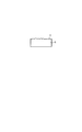
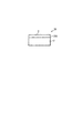
図2が概略的に示しているのは、ウェーハ又は基板1の図1のステップ104の後の状態であり、研削されたまま又はラッピングされたままのウェーハが、ステップ103及び104の軽減されたエッチング及び研磨ステップで処理されている。ウェーハ1の表面4の粗さは増大しておりその表面欠陥密度も増大している。
FIG. 2 schematically shows the state after
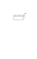
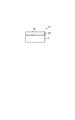
図3が概略的に示しているのは、図2のウェーハの図1のステップ105の後の状態であり、傾斜バッファ層2がウェーハ1上に成長してウェーハ20が形成されている。傾斜バッファ層2の材料はウェーハ基板1の材料とは異なる。ウェーハ1の表面4が粗く且つ欠陥を持っているにもかかわらず、傾斜バッファ層2は、非常に良好な結晶性を備えかつほとんど欠陥無くウェーハ1上に形成される。
FIG. 3 schematically shows the state of the wafer of FIG. 2 after
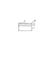
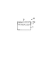
図4が概略的に示しているのは、図3のウェーハ20の図1のステップ106の後の状態であり、ウェーハ30が形成されている。ステップ106では、傾斜バッファ層2に緩和層3が非常に良好な結晶性でエピタキシャル成長する。緩和層3の表面5の表面粗さが増大している。
FIG. 4 schematically shows a state after the
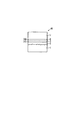
図5が概略的に示しているのは、図4の構造30の図1のステップ107、108、109の後の状態である。結果として生じる構造30’の表面8は平らで滑らかである。
FIG. 5 schematically shows the state after
図6が概略的に示しているのは、本発明の第2の実施形態に係る方法の工程の順序である。図1のステップ101〜109に図6のステップ110〜113が続く。図6のステップ110は緩和層3になされる注入ステップを示し、図7に示すように、緩和層3に脆弱化された領域6を形成する。脆弱化された領域6は緩和層3を2つの部分310,320に分ける。
FIG. 6 schematically shows the sequence of steps of the method according to the second embodiment of the present invention.
ステップ111には、図7に示されたウェーハ30’を、シリコンウェーハなどのハンドルウェーハ7とボンディングするステップが含まれる。ハンドルウェーハ7の平らな鏡面と、緩和層3の研磨され洗浄された表面5との間でボンディングは実施される。
Step 111 includes the step of bonding the
いわゆる「Smart‐cut(登録商標)工程」ステップであるステップ112で、機械的エネルギー、熱エネルギー、音響エネルギーや、光エネルギーなどのある一定の量のエネルギーが、図8のボンディングされた構造40に印加され、結果として、ボンディングされたウェーハ複合体40を、図9及び図12のウェーハ50及び60に示すように、2つの部分に分割又はカットする。
In
構造50、60の上部には、それぞれ、元の緩和層3の層部分310、320がある。分割のために、ウェーハ50、60のカットされたままの表面9、12の表面粗さは増大している。
On top of the
図6のステップ113では、ウェーハ50、60の緩和層部分310、320が更に厚くなるよう再成長させられ、結果として更に厚い緩和層321、311を備えたウェーハ51、61がもたらされる。図6のステップ114では、図10、13の構造51、61の表面10、13がCMP工程で研磨されその後洗浄され、結果として、図11及び図14に示されたウェーハ構造52、62に滑らかでほとんど欠陥のない表面11、14がもたらされる。
In
図7が概略的に示しているのは、図5のウェーハ30の図6の注入ステップ110の後の状態であり、緩和層3に脆弱化された領域6を備えたウェーハ30’がもたらされている。
FIG. 7 schematically shows the state after the
図8が概略的に示しているのは、図7のウェーハ30’の図6のボンディングステップ111の後の状態であり、ウェーハ30’がハンドルウェーハ7とボンディングされており、ボンディングされたウェーハ複合体40がもたらされている。
FIG. 8 schematically shows a state after the
図9及び図12が示しているのは、図8のウェーハ複合体40の部分の図6のステップ112でなされた分割後の状態である。分割ステップ112の間、ウェーハ複合体40は、所定の分割線を形成している脆弱化された領域6に沿って分割される。図9及び図12のウェーハ50、60の表面8、11が分割ステップにより生成されているので比較的粗い。ウェーハ50は、ハンドルウェーハ7と元の緩和層3の分割された部分320とからなる。図12のウェーハ60は、ウェーハ又は基板1と、傾斜バッファ層2と、分割された緩和層部分310とからなる。
FIG. 9 and FIG. 12 show a state after the division performed in
図10及び図13が概略的に示しているのは、緩和層部分320、310をより厚い緩和層部分321、311に再成長させた後の図9及び図12のウェーハである。
10 and 13 schematically illustrate the wafer of FIGS. 9 and 12 after the
図11及び図14が概略的に示しているのは、図10及び図13のウェーハ51、61の研磨及び洗浄の後の状態であり、最終ウェーハ構造52、62に平らでほとんど欠陥のない表面11、14がもたらされている。
FIGS. 11 and 14 schematically illustrate the state after polishing and cleaning of the
図1及び図6に示された全ての工程ステップについて考慮すべきなのは、該ステップは完全な工程フローの特徴的なステップを表しているだけであり、該ステップのみが使用できるとは主張していないことである。ステップとステップの間に、更なるステップ、例えば、洗浄、取り扱い、アニール、層堆積などのステップが適用できる。ウェーハ1上に傾斜バッファ層2の代わりに非傾斜層を成長させることも可能だが、考慮すべきなのは、層2は、その材料は何であれ、ウェーハ又は基板1の材料以外の材料でなければならないことである。
All of the process steps shown in FIGS. 1 and 6 should be considered only that they represent characteristic steps of the complete process flow and claim that only those steps can be used. It is not. Further steps can be applied between steps, such as cleaning, handling, annealing, layer deposition, etc. Although it is possible to grow a non-graded layer on the
全ての可能な工程フローで、鏡面研磨面を備えた従来市販されているウェーハとはその表面の品質に関し異なった、準備の整っていない基板上で、層2の成長が実施される。 In all possible process flows, the growth of layer 2 is carried out on an unprepared substrate that differs in surface quality from a conventionally marketed wafer with a mirror-polished surface.
1…基板、2…傾斜バッファ層、3…緩和層。
DESCRIPTION OF
Claims (11)
スライスされラッピングされ及び/又は研削されただけの準備の整っていない基板の表面に実施されるエッチングステップ(103)であって、軽減されたアルカリ性によるエッチングを含み、エッチングされた基板(1)の表面がより損傷を受けた状態とするエッチングステップと、1平方マイクロメートルのスキャンにつき0.2ナノメートルRMS未満の表面粗さを有する少なくとも1つのヘテロエピタキシャル層(2,3)の仕上げられた表面を形成する最終研磨ステップ(108)との間に、前記第2の材料の成長を実施することを特徴とする方法。 A substrate (1) of a single crystal first material and at least one layer (2, 2) of a second material epitaxially grown on the first material and having a lattice different from the lattice of the first material 3) and a method of manufacturing a wafer (52, 62) comprising:
An etching step (103) carried out on the surface of the substrate which is not ready to be sliced, lapped and / or ground , comprising a reduced alkaline etching of the etched substrate (1) An etching step that renders the surface more damaged and a finished surface of at least one heteroepitaxial layer (2,3) having a surface roughness of less than 0.2 nanometer RMS per square micrometer scan And performing a growth of the second material during a final polishing step (108) to form a substrate.
ことを特徴とする請求項1に記載の方法。 2. The second material is grown on a substrate (1) having a density of 0.2 to 1 surface defect density of defects larger than 0.12 micrometers per square millimeter. The method described.
前記第2の材料の前記少なくとも1つの層(2、3)が成長する前記基板(1)の表面は、スライスされラッピングされ及び/又は研削されただけの準備の整っていない基板の表面で、且つ、0.15ナノメートルRMS〜0.4ナノメートルRMSの表面粗さを有する表面であり、へテロエピタキシャル層である前記少なくとも1つの層(2、3)の表面(8)は研磨され、1平方マイクロメートルのスキャンにつき0.2ナノメートルRMS未満の表面粗さを有することを特徴とするウェーハ。 A substrate (1) of a single crystal first material and at least one layer (2, 2) of a second material epitaxially grown on the first material and having a lattice different from the lattice of the first material 3) and a wafer (52, 62) comprising:
The surface of the substrate (1) on which the at least one layer (2, 3) of the second material is grown is the surface of a substrate that is not ready to be sliced, lapped and / or ground; And the surface (8) of the at least one layer (2, 3), which is a surface having a surface roughness of 0.15 nanometer RMS to 0.4 nanometer RMS and is a heteroepitaxial layer, is polished; A wafer having a surface roughness of less than 0.2 nanometer RMS per scan of 1 micrometer.
Applications Claiming Priority (2)
| Application Number | Priority Date | Filing Date | Title |
|---|---|---|---|
| EP04291473A EP1605498A1 (en) | 2004-06-11 | 2004-06-11 | A method of manufacturing a semiconductor wafer |
| EP04291473.9 | 2004-06-11 |
Related Parent Applications (1)
| Application Number | Title | Priority Date | Filing Date |
|---|---|---|---|
| JP2005172558A Division JP2006054428A (en) | 2004-06-11 | 2005-06-13 | Method of manufacturing wafer |
Publications (2)
| Publication Number | Publication Date |
|---|---|
| JP2010045362A true JP2010045362A (en) | 2010-02-25 |
| JP5005740B2 JP5005740B2 (en) | 2012-08-22 |
Family
ID=34931173
Family Applications (2)
| Application Number | Title | Priority Date | Filing Date |
|---|---|---|---|
| JP2005172558A Withdrawn JP2006054428A (en) | 2004-06-11 | 2005-06-13 | Method of manufacturing wafer |
| JP2009186536A Active JP5005740B2 (en) | 2004-06-11 | 2009-08-11 | Wafer and wafer manufacturing method |
Family Applications Before (1)
| Application Number | Title | Priority Date | Filing Date |
|---|---|---|---|
| JP2005172558A Withdrawn JP2006054428A (en) | 2004-06-11 | 2005-06-13 | Method of manufacturing wafer |
Country Status (5)
| Country | Link |
|---|---|
| US (1) | US7138325B2 (en) |
| EP (1) | EP1605498A1 (en) |
| JP (2) | JP2006054428A (en) |
| KR (1) | KR100712042B1 (en) |
| CN (1) | CN100413028C (en) |
Families Citing this family (20)
| Publication number | Priority date | Publication date | Assignee | Title |
|---|---|---|---|---|
| US7175709B2 (en) * | 2004-05-17 | 2007-02-13 | Taiwan Semiconductor Manufacturing Co., Ltd. | Epitaxy layer and method of forming the same |
| US9685524B2 (en) | 2005-03-11 | 2017-06-20 | Vishay-Siliconix | Narrow semiconductor trench structure |
| TWI489557B (en) | 2005-12-22 | 2015-06-21 | Vishay Siliconix | High mobility p-channel trench and planar depletion-mode power metal-oxide semiconductor field-effect transistors |
| US8409954B2 (en) * | 2006-03-21 | 2013-04-02 | Vishay-Silconix | Ultra-low drain-source resistance power MOSFET |
| US8361337B2 (en) * | 2007-03-19 | 2013-01-29 | The University Of Massachusetts | Method of producing nanopatterned templates |
| US8981427B2 (en) | 2008-07-15 | 2015-03-17 | Taiwan Semiconductor Manufacturing Company, Ltd. | Polishing of small composite semiconductor materials |
| US8211737B2 (en) | 2008-09-19 | 2012-07-03 | The University Of Massachusetts | Method of producing nanopatterned articles, and articles produced thereby |
| US8247033B2 (en) * | 2008-09-19 | 2012-08-21 | The University Of Massachusetts | Self-assembly of block copolymers on topographically patterned polymeric substrates |
| US8518837B2 (en) * | 2008-09-25 | 2013-08-27 | The University Of Massachusetts | Method of producing nanopatterned articles using surface-reconstructed block copolymer films |
| US7927975B2 (en) | 2009-02-04 | 2011-04-19 | Micron Technology, Inc. | Semiconductor material manufacture |
| MY154627A (en) * | 2009-04-13 | 2015-07-15 | Sumco Corp | Method for producing silicon epitaxial wafer |
| JP5381304B2 (en) * | 2009-05-08 | 2014-01-08 | 株式会社Sumco | Manufacturing method of silicon epitaxial wafer |
| US9012253B2 (en) * | 2009-12-16 | 2015-04-21 | Micron Technology, Inc. | Gallium nitride wafer substrate for solid state lighting devices, and associated systems and methods |
| US9455146B2 (en) * | 2009-12-17 | 2016-09-27 | California Institute Of Technology | Virtual substrates for epitaxial growth and methods of making the same |
| TWI510682B (en) * | 2011-01-28 | 2015-12-01 | Sino American Silicon Prod Inc | Modification process for nano-structuring ingot surface, wafer manufacturing method and wafer thereof |
| US9156682B2 (en) | 2011-05-25 | 2015-10-13 | The University Of Massachusetts | Method of forming oriented block copolymer line patterns, block copolymer line patterns formed thereby, and their use to form patterned articles |
| US8492187B2 (en) | 2011-09-29 | 2013-07-23 | International Business Machines Corporation | High throughput epitaxial liftoff for releasing multiple semiconductor device layers from a single base substrate |
| US9412883B2 (en) | 2011-11-22 | 2016-08-09 | Taiwan Semiconductor Manufacturing Company, Ltd. | Methods and apparatus for MOS capacitors in replacement gate process |
| US11515408B2 (en) * | 2020-03-02 | 2022-11-29 | Taiwan Semiconductor Manufacturing Company, Ltd. | Rough buffer layer for group III-V devices on silicon |
| US11555250B2 (en) | 2020-04-29 | 2023-01-17 | Applied Materials, Inc. | Organic contamination free surface machining |
Citations (12)
| Publication number | Priority date | Publication date | Assignee | Title |
|---|---|---|---|---|
| JPS5051668A (en) * | 1973-08-21 | 1975-05-08 | ||
| JPH10172976A (en) * | 1996-12-12 | 1998-06-26 | Mitsubishi Materials Shilicon Corp | Manufacture of epitaxial wafer with eg layer |
| JPH11135792A (en) * | 1997-10-27 | 1999-05-21 | Sony Corp | Manufacture of semiconductor device |
| JP2000243699A (en) * | 1999-02-23 | 2000-09-08 | Hitachi Ltd | Manufacture of semiconductor wafer, and manufacture of semiconductor device |
| JP2001223163A (en) * | 2000-02-09 | 2001-08-17 | Shin Etsu Handotai Co Ltd | Silicon epitaxial wafer and method of manufacturing the same |
| JP2001257243A (en) * | 2000-03-09 | 2001-09-21 | Mitsubishi Materials Silicon Corp | Method for measurig fine particle on silicon wafer surface |
| JP2002289611A (en) * | 2001-03-26 | 2002-10-04 | Toshiba Corp | Manufacturing method and manufacturing apparatus of semiconductor device |
| JP2003142686A (en) * | 2001-11-07 | 2003-05-16 | Sumitomo Mitsubishi Silicon Corp | Method of manufacturing semiconductor substrate, method of manufacturing field effect transistor, and semiconductor substrate and field effect transistor |
| JP2003158075A (en) * | 2001-08-23 | 2003-05-30 | Sumitomo Mitsubishi Silicon Corp | Method for manufacturing semiconductor substrate, method for manufacturing field effect transistor, semiconductor substrate and field effect transistor |
| JP2003243404A (en) * | 2002-02-21 | 2003-08-29 | Shin Etsu Handotai Co Ltd | Method of manufacturing annealed wafer and annealed wafer |
| JP2003347399A (en) * | 2002-05-23 | 2003-12-05 | Sharp Corp | Method of manufacturing semiconductor substrate |
| JP2004342818A (en) * | 2003-05-15 | 2004-12-02 | Toshiba Ceramics Co Ltd | Method of producing semiconductor substrate |
Family Cites Families (11)
| Publication number | Priority date | Publication date | Assignee | Title |
|---|---|---|---|---|
| TW230822B (en) * | 1993-03-02 | 1994-09-21 | Sumitomo Electric Industries | |
| JP3120825B2 (en) * | 1994-11-14 | 2000-12-25 | 信越半導体株式会社 | Epitaxial wafer and method for manufacturing the same |
| US6039803A (en) * | 1996-06-28 | 2000-03-21 | Massachusetts Institute Of Technology | Utilization of miscut substrates to improve relaxed graded silicon-germanium and germanium layers on silicon |
| US6174727B1 (en) * | 1998-11-03 | 2001-01-16 | Komatsu Electronic Metals, Co. | Method of detecting microscopic defects existing on a silicon wafer |
| JP3943782B2 (en) * | 1999-11-29 | 2007-07-11 | 信越半導体株式会社 | Reclaimed wafer reclaim processing method and reclaimed peeled wafer |
| WO2001043174A2 (en) * | 1999-12-13 | 2001-06-14 | North Carolina State University | Fabrication of gallium nitride layers on textured silicon substrates |
| DE19960823B4 (en) | 1999-12-16 | 2007-04-12 | Siltronic Ag | Process for the production of an epitaxated semiconductor wafer and its use |
| US6488767B1 (en) * | 2001-06-08 | 2002-12-03 | Advanced Technology Materials, Inc. | High surface quality GaN wafer and method of fabricating same |
| US6995427B2 (en) * | 2003-01-29 | 2006-02-07 | S.O.I.Tec Silicon On Insulator Technologies S.A. | Semiconductor structure for providing strained crystalline layer on insulator and method for fabricating same |
| DE60323098D1 (en) * | 2003-09-26 | 2008-10-02 | Soitec Silicon On Insulator | Process for the preparation of substrates for epitaxial growth |
| EP1571241A1 (en) * | 2004-03-01 | 2005-09-07 | S.O.I.T.E.C. Silicon on Insulator Technologies | Method of manufacturing a wafer |
-
2004
- 2004-06-11 EP EP04291473A patent/EP1605498A1/en not_active Withdrawn
- 2004-12-03 US US11/004,410 patent/US7138325B2/en active Active
-
2005
- 2005-06-10 KR KR1020050049858A patent/KR100712042B1/en active IP Right Grant
- 2005-06-10 CN CNB2005100753492A patent/CN100413028C/en active Active
- 2005-06-13 JP JP2005172558A patent/JP2006054428A/en not_active Withdrawn
-
2009
- 2009-08-11 JP JP2009186536A patent/JP5005740B2/en active Active
Patent Citations (12)
| Publication number | Priority date | Publication date | Assignee | Title |
|---|---|---|---|---|
| JPS5051668A (en) * | 1973-08-21 | 1975-05-08 | ||
| JPH10172976A (en) * | 1996-12-12 | 1998-06-26 | Mitsubishi Materials Shilicon Corp | Manufacture of epitaxial wafer with eg layer |
| JPH11135792A (en) * | 1997-10-27 | 1999-05-21 | Sony Corp | Manufacture of semiconductor device |
| JP2000243699A (en) * | 1999-02-23 | 2000-09-08 | Hitachi Ltd | Manufacture of semiconductor wafer, and manufacture of semiconductor device |
| JP2001223163A (en) * | 2000-02-09 | 2001-08-17 | Shin Etsu Handotai Co Ltd | Silicon epitaxial wafer and method of manufacturing the same |
| JP2001257243A (en) * | 2000-03-09 | 2001-09-21 | Mitsubishi Materials Silicon Corp | Method for measurig fine particle on silicon wafer surface |
| JP2002289611A (en) * | 2001-03-26 | 2002-10-04 | Toshiba Corp | Manufacturing method and manufacturing apparatus of semiconductor device |
| JP2003158075A (en) * | 2001-08-23 | 2003-05-30 | Sumitomo Mitsubishi Silicon Corp | Method for manufacturing semiconductor substrate, method for manufacturing field effect transistor, semiconductor substrate and field effect transistor |
| JP2003142686A (en) * | 2001-11-07 | 2003-05-16 | Sumitomo Mitsubishi Silicon Corp | Method of manufacturing semiconductor substrate, method of manufacturing field effect transistor, and semiconductor substrate and field effect transistor |
| JP2003243404A (en) * | 2002-02-21 | 2003-08-29 | Shin Etsu Handotai Co Ltd | Method of manufacturing annealed wafer and annealed wafer |
| JP2003347399A (en) * | 2002-05-23 | 2003-12-05 | Sharp Corp | Method of manufacturing semiconductor substrate |
| JP2004342818A (en) * | 2003-05-15 | 2004-12-02 | Toshiba Ceramics Co Ltd | Method of producing semiconductor substrate |
Also Published As
| Publication number | Publication date |
|---|---|
| CN100413028C (en) | 2008-08-20 |
| US7138325B2 (en) | 2006-11-21 |
| CN1722367A (en) | 2006-01-18 |
| KR20060048325A (en) | 2006-05-18 |
| KR100712042B1 (en) | 2007-04-27 |
| US20050277278A1 (en) | 2005-12-15 |
| JP2006054428A (en) | 2006-02-23 |
| EP1605498A1 (en) | 2005-12-14 |
| JP5005740B2 (en) | 2012-08-22 |
Similar Documents
| Publication | Publication Date | Title |
|---|---|---|
| JP5005740B2 (en) | Wafer and wafer manufacturing method | |
| JP4388741B2 (en) | Method for transferring semiconductor thin layer and method for manufacturing donor wafer used therefor | |
| KR100746182B1 (en) | A method for manufacturing compound material wafers | |
| US8154022B2 (en) | Process for fabricating a structure for epitaxy without an exclusion zone | |
| KR100746179B1 (en) | A method of preparation of an epitaxial substrate | |
| WO2017047478A1 (en) | SiC COMPOSITE SUBSTRATE AND METHOD FOR MANUFACTURING SAME | |
| JP6626583B2 (en) | Semiconductor wafer and method for polishing semiconductor wafer | |
| JP2006222453A (en) | Silicon wafer, method for manufacturing the same, and soi wafer | |
| WO2017047508A1 (en) | METHOD FOR PRODUCING SiC COMPOSITE SUBSTRATE | |
| US20030060020A1 (en) | Method and apparatus for finishing substrates for wafer to wafer bonding | |
| US7261777B2 (en) | Method for fabricating an epitaxial substrate | |
| JP2010171330A (en) | Method of manufacturing epitaxial wafer, defect removing method, and the epitaxial wafer | |
| JP2009051678A (en) | Manufacturing method of sapphire substrate | |
| US9768057B2 (en) | Method for transferring a layer from a single-crystal substrate | |
| JP2004165484A (en) | Processing method for semiconductor wafer |
Legal Events
| Date | Code | Title | Description |
|---|---|---|---|
| A977 | Report on retrieval |
Free format text: JAPANESE INTERMEDIATE CODE: A971007 Effective date: 20101119 |
|
| A131 | Notification of reasons for refusal |
Free format text: JAPANESE INTERMEDIATE CODE: A131 Effective date: 20101130 |
|
| A521 | Request for written amendment filed |
Free format text: JAPANESE INTERMEDIATE CODE: A523 Effective date: 20110221 |
|
| A02 | Decision of refusal |
Free format text: JAPANESE INTERMEDIATE CODE: A02 Effective date: 20111129 |
|
| A521 | Request for written amendment filed |
Free format text: JAPANESE INTERMEDIATE CODE: A523 Effective date: 20120131 |
|
| A911 | Transfer to examiner for re-examination before appeal (zenchi) |
Free format text: JAPANESE INTERMEDIATE CODE: A911 Effective date: 20120229 |
|
| A131 | Notification of reasons for refusal |
Free format text: JAPANESE INTERMEDIATE CODE: A131 Effective date: 20120321 |
|
| A521 | Request for written amendment filed |
Free format text: JAPANESE INTERMEDIATE CODE: A523 Effective date: 20120323 |
|
| TRDD | Decision of grant or rejection written | ||
| A01 | Written decision to grant a patent or to grant a registration (utility model) |
Free format text: JAPANESE INTERMEDIATE CODE: A01 Effective date: 20120508 |
|
| A01 | Written decision to grant a patent or to grant a registration (utility model) |
Free format text: JAPANESE INTERMEDIATE CODE: A01 |
|
| A61 | First payment of annual fees (during grant procedure) |
Free format text: JAPANESE INTERMEDIATE CODE: A61 Effective date: 20120523 |
|
| FPAY | Renewal fee payment (event date is renewal date of database) |
Free format text: PAYMENT UNTIL: 20150601 Year of fee payment: 3 |
|
| R150 | Certificate of patent or registration of utility model |
Free format text: JAPANESE INTERMEDIATE CODE: R150 Ref document number: 5005740 Country of ref document: JP Free format text: JAPANESE INTERMEDIATE CODE: R150 |
|
| R250 | Receipt of annual fees |
Free format text: JAPANESE INTERMEDIATE CODE: R250 |
|
| R250 | Receipt of annual fees |
Free format text: JAPANESE INTERMEDIATE CODE: R250 |
|
| R250 | Receipt of annual fees |
Free format text: JAPANESE INTERMEDIATE CODE: R250 |
|
| R250 | Receipt of annual fees |
Free format text: JAPANESE INTERMEDIATE CODE: R250 |
|
| R250 | Receipt of annual fees |
Free format text: JAPANESE INTERMEDIATE CODE: R250 |
|
| R250 | Receipt of annual fees |
Free format text: JAPANESE INTERMEDIATE CODE: R250 |
|
| R250 | Receipt of annual fees |
Free format text: JAPANESE INTERMEDIATE CODE: R250 |
|
| R250 | Receipt of annual fees |
Free format text: JAPANESE INTERMEDIATE CODE: R250 |
|
| R250 | Receipt of annual fees |
Free format text: JAPANESE INTERMEDIATE CODE: R250 |