JP2010040977A - 半導体記憶装置及びその製造方法 - Google Patents
半導体記憶装置及びその製造方法 Download PDFInfo
- Publication number
- JP2010040977A JP2010040977A JP2008205339A JP2008205339A JP2010040977A JP 2010040977 A JP2010040977 A JP 2010040977A JP 2008205339 A JP2008205339 A JP 2008205339A JP 2008205339 A JP2008205339 A JP 2008205339A JP 2010040977 A JP2010040977 A JP 2010040977A
- Authority
- JP
- Japan
- Prior art keywords
- contact
- wirings
- cell array
- contact plug
- bit line
- Prior art date
- Legal status (The legal status is an assumption and is not a legal conclusion. Google has not performed a legal analysis and makes no representation as to the accuracy of the status listed.)
- Granted
Links
Images


Classifications
-
- H—ELECTRICITY
- H10—SEMICONDUCTOR DEVICES; ELECTRIC SOLID-STATE DEVICES NOT OTHERWISE PROVIDED FOR
- H10B—ELECTRONIC MEMORY DEVICES
- H10B63/00—Resistance change memory devices, e.g. resistive RAM [ReRAM] devices
- H10B63/20—Resistance change memory devices, e.g. resistive RAM [ReRAM] devices comprising selection components having two electrodes, e.g. diodes
-
- G—PHYSICS
- G11—INFORMATION STORAGE
- G11C—STATIC STORES
- G11C13/00—Digital stores characterised by the use of storage elements not covered by groups G11C11/00, G11C23/00, or G11C25/00
- G11C13/0002—Digital stores characterised by the use of storage elements not covered by groups G11C11/00, G11C23/00, or G11C25/00 using resistive RAM [RRAM] elements
- G11C13/0007—Digital stores characterised by the use of storage elements not covered by groups G11C11/00, G11C23/00, or G11C25/00 using resistive RAM [RRAM] elements comprising metal oxide memory material, e.g. perovskites
-
- G—PHYSICS
- G11—INFORMATION STORAGE
- G11C—STATIC STORES
- G11C13/00—Digital stores characterised by the use of storage elements not covered by groups G11C11/00, G11C23/00, or G11C25/00
- G11C13/0002—Digital stores characterised by the use of storage elements not covered by groups G11C11/00, G11C23/00, or G11C25/00 using resistive RAM [RRAM] elements
- G11C13/0009—RRAM elements whose operation depends upon chemical change
- G11C13/0011—RRAM elements whose operation depends upon chemical change comprising conductive bridging RAM [CBRAM] or programming metallization cells [PMCs]
-
- H—ELECTRICITY
- H10—SEMICONDUCTOR DEVICES; ELECTRIC SOLID-STATE DEVICES NOT OTHERWISE PROVIDED FOR
- H10B—ELECTRONIC MEMORY DEVICES
- H10B63/00—Resistance change memory devices, e.g. resistive RAM [ReRAM] devices
- H10B63/80—Arrangements comprising multiple bistable or multi-stable switching components of the same type on a plane parallel to the substrate, e.g. cross-point arrays
- H10B63/84—Arrangements comprising multiple bistable or multi-stable switching components of the same type on a plane parallel to the substrate, e.g. cross-point arrays arranged in a direction perpendicular to the substrate, e.g. 3D cell arrays
-
- G—PHYSICS
- G11—INFORMATION STORAGE
- G11C—STATIC STORES
- G11C13/00—Digital stores characterised by the use of storage elements not covered by groups G11C11/00, G11C23/00, or G11C25/00
- G11C13/0002—Digital stores characterised by the use of storage elements not covered by groups G11C11/00, G11C23/00, or G11C25/00 using resistive RAM [RRAM] elements
- G11C13/0004—Digital stores characterised by the use of storage elements not covered by groups G11C11/00, G11C23/00, or G11C25/00 using resistive RAM [RRAM] elements comprising amorphous/crystalline phase transition cells
-
- G—PHYSICS
- G11—INFORMATION STORAGE
- G11C—STATIC STORES
- G11C2213/00—Indexing scheme relating to G11C13/00 for features not covered by this group
- G11C2213/30—Resistive cell, memory material aspects
- G11C2213/31—Material having complex metal oxide, e.g. perovskite structure
-
- G—PHYSICS
- G11—INFORMATION STORAGE
- G11C—STATIC STORES
- G11C2213/00—Indexing scheme relating to G11C13/00 for features not covered by this group
- G11C2213/70—Resistive array aspects
- G11C2213/71—Three dimensional array
-
- H—ELECTRICITY
- H10—SEMICONDUCTOR DEVICES; ELECTRIC SOLID-STATE DEVICES NOT OTHERWISE PROVIDED FOR
- H10N—ELECTRIC SOLID-STATE DEVICES NOT OTHERWISE PROVIDED FOR
- H10N70/00—Solid-state devices having no potential barriers, and specially adapted for rectifying, amplifying, oscillating or switching
- H10N70/011—Manufacture or treatment of multistable switching devices
- H10N70/061—Shaping switching materials
- H10N70/063—Shaping switching materials by etching of pre-deposited switching material layers, e.g. lithography
-
- H—ELECTRICITY
- H10—SEMICONDUCTOR DEVICES; ELECTRIC SOLID-STATE DEVICES NOT OTHERWISE PROVIDED FOR
- H10N—ELECTRIC SOLID-STATE DEVICES NOT OTHERWISE PROVIDED FOR
- H10N70/00—Solid-state devices having no potential barriers, and specially adapted for rectifying, amplifying, oscillating or switching
- H10N70/20—Multistable switching devices, e.g. memristors
- H10N70/24—Multistable switching devices, e.g. memristors based on migration or redistribution of ionic species, e.g. anions, vacancies
- H10N70/245—Multistable switching devices, e.g. memristors based on migration or redistribution of ionic species, e.g. anions, vacancies the species being metal cations, e.g. programmable metallization cells
-
- H—ELECTRICITY
- H10—SEMICONDUCTOR DEVICES; ELECTRIC SOLID-STATE DEVICES NOT OTHERWISE PROVIDED FOR
- H10N—ELECTRIC SOLID-STATE DEVICES NOT OTHERWISE PROVIDED FOR
- H10N70/00—Solid-state devices having no potential barriers, and specially adapted for rectifying, amplifying, oscillating or switching
- H10N70/801—Constructional details of multistable switching devices
- H10N70/821—Device geometry
- H10N70/826—Device geometry adapted for essentially vertical current flow, e.g. sandwich or pillar type devices
-
- H—ELECTRICITY
- H10—SEMICONDUCTOR DEVICES; ELECTRIC SOLID-STATE DEVICES NOT OTHERWISE PROVIDED FOR
- H10N—ELECTRIC SOLID-STATE DEVICES NOT OTHERWISE PROVIDED FOR
- H10N70/00—Solid-state devices having no potential barriers, and specially adapted for rectifying, amplifying, oscillating or switching
- H10N70/801—Constructional details of multistable switching devices
- H10N70/881—Switching materials
- H10N70/883—Oxides or nitrides
- H10N70/8836—Complex metal oxides, e.g. perovskites, spinels
Landscapes
- Chemical & Material Sciences (AREA)
- Engineering & Computer Science (AREA)
- Materials Engineering (AREA)
- Semiconductor Memories (AREA)
Abstract
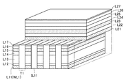
【解決手段】半導体基板と、この半導体基板上に形成されて、複数の第1の配線、これら複数の第1の配線と交差する複数の第2の配線、及び前記第1及び第2の配線の交差部で両配線間に接続されたメモリセルを有するセルアレイ層を複数積層してなるセルアレイブロックと、複数の前記セルアレイ層の複数の第1の配線間、複数の第2の配線間、前記第1若しくは第2の配線及び前記半導体基板間、又は前記第1若しくは第2の配線及び他の金属配線間を接続する前記セルアレイ層の積層方向に延びる複数のコンタクトプラグとを備え、所定の前記セルアレイ層の第1又は第2の配線は、前記コンタクトプラグの両側面と接触するコンタクト接続部が形成されている
【選択図】図7
Description
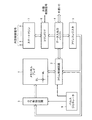
図1は、本発明の第1の実施形態に係る半導体記憶装置のブロック図である。
次に、ビット線BL及びワード線WLの端部の形状について説明する。

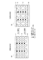
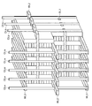
図9〜図20は、ワード線WL1以上の形成工程を工程順に示した斜視図である。これら図9〜図20を適宜参照しながら、上層部の形成プロセスを説明する。なお、説明の便宜上、一部の絶縁体は図示を省略している。
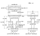
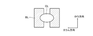
図21、22は、本発明の第2の実施形態に係る半導体記憶装置のコンタクト接続部とコンタクトプラグの形状であり、半導体記憶装置の積層方向を面法線とする断面形状を示す図である。
図23、24は、本発明の第3の実施形態に係る半導体記憶装置のコンタクト接続部及びコンタクトプラグを示す図であり、半導体記憶装置の積層方向を面法線とする断面形状である。
〜BL208を接続するものであり、コンタクトプラグCLbとビット線BL207との接触面積s207a、s207bの総和、コンタクトプラグCLbとビット線BL206との接触面積s206a、s206bの総和、コンタクトプラグCLbとビット線BL205の接触面積s205が同じになっている。この場合も、図23の場合と同様、コンタクトプラグCLb及びビット線BL205〜BL207の各接続抵抗を同じにすることができる。
Claims (5)
- 半導体基板と、
この半導体基板上に形成されて、複数の第1の配線、これら複数の第1の配線と交差する複数の第2の配線、及び前記第1及び第2の配線の交差部で両配線間に接続されたメモリセルを有するセルアレイ層を複数積層してなるセルアレイブロックと、
複数の前記セルアレイ層の複数の第1の配線間、複数の第2の配線間、前記第1若しくは第2の配線及び前記半導体基板間、又は前記第1若しくは第2の配線及び他の金属配線間を接続する前記セルアレイ層の積層方向に延びる複数のコンタクトプラグと
を備え、
所定の前記セルアレイ層の第1又は第2の配線は、前記コンタクトプラグの両側面と接触するコンタクト接続部が形成されている
ことを特徴とする半導体記憶装置。 - 前記コンタクトプラグは、前記セルアレイの積層方向と直交する断面が円形状である
ことを特徴とする請求項1記載の半導体記憶装置。 - 前記コンタクトプラグは、前記セルアレイの積層方向と直交する断面が楕円形状である
ことを特徴とする請求項1記載の半導体記憶装置。 - 前記コンタクトプラグと前記半導体基板及び前記セルアレイ層の第1又は第2の配線との複数ある接触部分のうち少なくとも2箇所の接触面積が同一である
ことを特徴とする請求項1〜3記載のいずれか1項記載の半導体記憶装置。 - 半導体基板上に、互いに交差する第1及び第2の配線とこれら第1及び第2の配線の各交差部で両配線間に接続されたメモリセルを備えたセルアレイ層を複数多層に形成する工程と、
所定の間隙を持つ2つの凸形状を有するマスクを用い、前記第1及び第2の配線にコンタクト接続部を形成する工程と、
複数の前記セルアレイ層に形成された前記コンタクト接続部の間隙を貫通する貫通孔を形成する工程と、
形成された前記貫通孔に導電性材料を充填して前記各セルアレイ層の前記第1又は第2の配線と前記半導体基板とをそれぞれ個別に接続する前記セルアレイ層の積層方向に延びる複数のコンタクトプラグを形成する工程と
を有することを特徴とする半導体記憶装置の製造方法。
Priority Applications (2)
| Application Number | Priority Date | Filing Date | Title |
|---|---|---|---|
| JP2008205339A JP5288933B2 (ja) | 2008-08-08 | 2008-08-08 | 半導体記憶装置及びその製造方法 |
| US12/399,376 US8222677B2 (en) | 2008-08-08 | 2009-03-06 | Semiconductor memory device and method of manufacturing the same |
Applications Claiming Priority (1)
| Application Number | Priority Date | Filing Date | Title |
|---|---|---|---|
| JP2008205339A JP5288933B2 (ja) | 2008-08-08 | 2008-08-08 | 半導体記憶装置及びその製造方法 |
Publications (2)
| Publication Number | Publication Date |
|---|---|
| JP2010040977A true JP2010040977A (ja) | 2010-02-18 |
| JP5288933B2 JP5288933B2 (ja) | 2013-09-11 |
Family
ID=41652077
Family Applications (1)
| Application Number | Title | Priority Date | Filing Date |
|---|---|---|---|
| JP2008205339A Expired - Fee Related JP5288933B2 (ja) | 2008-08-08 | 2008-08-08 | 半導体記憶装置及びその製造方法 |
Country Status (2)
| Country | Link |
|---|---|
| US (1) | US8222677B2 (ja) |
| JP (1) | JP5288933B2 (ja) |
Cited By (5)
| Publication number | Priority date | Publication date | Assignee | Title |
|---|---|---|---|---|
| JP2011054758A (ja) * | 2009-09-02 | 2011-03-17 | Toshiba Corp | 半導体集積回路装置 |
| JP2011243705A (ja) * | 2010-05-17 | 2011-12-01 | Toshiba Corp | 半導体装置 |
| JP2012248620A (ja) * | 2011-05-26 | 2012-12-13 | Toshiba Corp | 半導体記憶装置の製造方法 |
| US8441040B2 (en) | 2009-09-24 | 2013-05-14 | Kabushiki Kaisha Toshiba | Semiconductor memory device |
| WO2020188775A1 (ja) * | 2019-03-19 | 2020-09-24 | キオクシア株式会社 | 半導体記憶装置 |
Families Citing this family (19)
| Publication number | Priority date | Publication date | Assignee | Title |
|---|---|---|---|---|
| JP2011176226A (ja) * | 2010-02-25 | 2011-09-08 | Toshiba Corp | 半導体記憶装置及びその製造方法 |
| US8258020B2 (en) * | 2010-11-04 | 2012-09-04 | Crossbar Inc. | Interconnects for stacked non-volatile memory device and method |
| JP5595977B2 (ja) * | 2011-05-27 | 2014-09-24 | 株式会社東芝 | 半導体記憶装置、その製造方法及びコンタクト構造の形成方法 |
| US8728940B2 (en) * | 2012-01-26 | 2014-05-20 | Micron Technology, Inc. | Memory arrays and methods of forming same |
| JP5606479B2 (ja) * | 2012-03-22 | 2014-10-15 | 株式会社東芝 | 半導体記憶装置 |
| US10043852B2 (en) * | 2015-08-11 | 2018-08-07 | Toshiba Memory Corporation | Magnetoresistive memory device and manufacturing method of the same |
| FR3055943B1 (fr) * | 2016-09-15 | 2020-10-02 | Valeo Vision | Cablage d'une source lumineuse de haute resolution |
| US10777510B2 (en) | 2016-11-28 | 2020-09-15 | Taiwan Semiconductor Manufacturing Co., Ltd. | Semiconductor device including dummy via anchored to dummy metal layer |
| JP2018148071A (ja) * | 2017-03-07 | 2018-09-20 | 東芝メモリ株式会社 | 記憶装置 |
| US10424374B2 (en) | 2017-04-28 | 2019-09-24 | Micron Technology, Inc. | Programming enhancement in self-selecting memory |
| US10424730B2 (en) | 2018-02-09 | 2019-09-24 | Micron Technology, Inc. | Tapered memory cell profiles |
| US10541364B2 (en) | 2018-02-09 | 2020-01-21 | Micron Technology, Inc. | Memory cells with asymmetrical electrode interfaces |
| US10693065B2 (en) | 2018-02-09 | 2020-06-23 | Micron Technology, Inc. | Tapered cell profile and fabrication |
| US10854813B2 (en) | 2018-02-09 | 2020-12-01 | Micron Technology, Inc. | Dopant-modulated etching for memory devices |
| US10985212B2 (en) | 2019-04-16 | 2021-04-20 | Micron Technology, Inc. | Multi-component cell architectures for a memory device |
| JP2021048167A (ja) | 2019-09-17 | 2021-03-25 | キオクシア株式会社 | 半導体記憶装置 |
| KR102773656B1 (ko) | 2019-10-23 | 2025-02-28 | 삼성전자주식회사 | 가변 저항 메모리 장치 |
| US11715520B2 (en) * | 2021-04-05 | 2023-08-01 | Micron Technology, Inc. | Socket structure for spike current suppression in a memory array |
| US11514985B2 (en) | 2021-04-05 | 2022-11-29 | Micron Technology, Inc. | Spike current suppression in a memory array |
Citations (5)
| Publication number | Priority date | Publication date | Assignee | Title |
|---|---|---|---|---|
| JPH09120964A (ja) * | 1995-10-26 | 1997-05-06 | Matsushita Electric Ind Co Ltd | 配線の形成方法及び半導体素子の形成方法 |
| JP2001102541A (ja) * | 1999-09-28 | 2001-04-13 | Toshiba Corp | 半導体記憶装置とその製造方法 |
| JP2006512776A (ja) * | 2002-12-31 | 2006-04-13 | マトリックス セミコンダクター インコーポレイテッド | 直列接続されたトランジスタ列を組込んだプログラマブルメモリアレイ構造およびこの構造を製造して作動させるための方法 |
| JP2006514393A (ja) * | 2003-03-18 | 2006-04-27 | 株式会社東芝 | プログラマブル抵抗メモリ装置 |
| JP2008098461A (ja) * | 2006-10-13 | 2008-04-24 | Renesas Technology Corp | 半導体装置 |
Family Cites Families (7)
| Publication number | Priority date | Publication date | Assignee | Title |
|---|---|---|---|---|
| US377044A (en) * | 1888-01-31 | Henby g | ||
| US376359A (en) * | 1888-01-10 | Sash-fastener | ||
| US338946A (en) * | 1886-03-30 | Stem winding and setting watch | ||
| US6313026B1 (en) * | 2000-04-10 | 2001-11-06 | Micron Technology, Inc. | Microelectronic contacts and methods for producing same |
| US6365419B1 (en) * | 2000-08-28 | 2002-04-02 | Motorola, Inc. | High density MRAM cell array |
| JP5016928B2 (ja) * | 2007-01-10 | 2012-09-05 | 株式会社東芝 | 不揮発性半導体記憶装置及びその製造方法 |
| JP5550239B2 (ja) | 2009-01-26 | 2014-07-16 | 株式会社東芝 | 不揮発性半導体記憶装置、及びその製造方法 |
-
2008
- 2008-08-08 JP JP2008205339A patent/JP5288933B2/ja not_active Expired - Fee Related
-
2009
- 2009-03-06 US US12/399,376 patent/US8222677B2/en active Active
Patent Citations (5)
| Publication number | Priority date | Publication date | Assignee | Title |
|---|---|---|---|---|
| JPH09120964A (ja) * | 1995-10-26 | 1997-05-06 | Matsushita Electric Ind Co Ltd | 配線の形成方法及び半導体素子の形成方法 |
| JP2001102541A (ja) * | 1999-09-28 | 2001-04-13 | Toshiba Corp | 半導体記憶装置とその製造方法 |
| JP2006512776A (ja) * | 2002-12-31 | 2006-04-13 | マトリックス セミコンダクター インコーポレイテッド | 直列接続されたトランジスタ列を組込んだプログラマブルメモリアレイ構造およびこの構造を製造して作動させるための方法 |
| JP2006514393A (ja) * | 2003-03-18 | 2006-04-27 | 株式会社東芝 | プログラマブル抵抗メモリ装置 |
| JP2008098461A (ja) * | 2006-10-13 | 2008-04-24 | Renesas Technology Corp | 半導体装置 |
Cited By (10)
| Publication number | Priority date | Publication date | Assignee | Title |
|---|---|---|---|---|
| JP2011054758A (ja) * | 2009-09-02 | 2011-03-17 | Toshiba Corp | 半導体集積回路装置 |
| US8274068B2 (en) | 2009-09-02 | 2012-09-25 | Kabushiki Kaisha Toshiba | Semiconductor integrated circuit device and method of fabricating the same |
| US8441040B2 (en) | 2009-09-24 | 2013-05-14 | Kabushiki Kaisha Toshiba | Semiconductor memory device |
| JP2011243705A (ja) * | 2010-05-17 | 2011-12-01 | Toshiba Corp | 半導体装置 |
| US8791446B2 (en) | 2010-05-17 | 2014-07-29 | Kabushiki Kaisha Toshiba | Semiconductor device |
| JP2012248620A (ja) * | 2011-05-26 | 2012-12-13 | Toshiba Corp | 半導体記憶装置の製造方法 |
| WO2020188775A1 (ja) * | 2019-03-19 | 2020-09-24 | キオクシア株式会社 | 半導体記憶装置 |
| JPWO2020188775A1 (ja) * | 2019-03-19 | 2021-10-21 | キオクシア株式会社 | 半導体記憶装置 |
| JP7214835B2 (ja) | 2019-03-19 | 2023-01-30 | キオクシア株式会社 | 半導体記憶装置 |
| US11984394B2 (en) | 2019-03-19 | 2024-05-14 | Kioxia Corporation | Semiconductor memory device having contact plugs extend in the stacking direction of the plurality of the first and second conductive layers |
Also Published As
| Publication number | Publication date |
|---|---|
| US20100032725A1 (en) | 2010-02-11 |
| JP5288933B2 (ja) | 2013-09-11 |
| US8222677B2 (en) | 2012-07-17 |
Similar Documents
| Publication | Publication Date | Title |
|---|---|---|
| JP5288933B2 (ja) | 半導体記憶装置及びその製造方法 | |
| JP5550239B2 (ja) | 不揮発性半導体記憶装置、及びその製造方法 | |
| US8441040B2 (en) | Semiconductor memory device | |
| JP5175526B2 (ja) | 不揮発性半導体記憶装置及びその製造方法 | |
| KR101015325B1 (ko) | 반도체 기억 장치 | |
| JP5322533B2 (ja) | 不揮発性半導体記憶装置、及びその製造方法 | |
| KR101128620B1 (ko) | 불휘발성 반도체 기억 장치 및 그 제조 방법 | |
| JP5159270B2 (ja) | 不揮発性半導体記憶装置及びその製造方法 | |
| JP2009130139A (ja) | 不揮発性半導体記憶装置の製造方法 | |
| JP2010165803A (ja) | 半導体記憶装置の製造方法及び半導体記憶装置 | |
| JP2012248620A (ja) | 半導体記憶装置の製造方法 | |
| KR20190119180A (ko) | 3차원 메모리 어레이 | |
| JP2011129737A (ja) | 半導体記憶装置の製造方法及び半導体記憶装置 | |
| JP2010192718A (ja) | 不揮発性半導体記憶装置及びその製造方法 | |
| JP5279879B2 (ja) | 不揮発性半導体記憶装置 |
Legal Events
| Date | Code | Title | Description |
|---|---|---|---|
| A621 | Written request for application examination |
Free format text: JAPANESE INTERMEDIATE CODE: A621 Effective date: 20100915 |
|
| A131 | Notification of reasons for refusal |
Free format text: JAPANESE INTERMEDIATE CODE: A131 Effective date: 20121218 |
|
| A977 | Report on retrieval |
Free format text: JAPANESE INTERMEDIATE CODE: A971007 Effective date: 20121220 |
|
| A521 | Request for written amendment filed |
Free format text: JAPANESE INTERMEDIATE CODE: A523 Effective date: 20130218 |
|
| RD01 | Notification of change of attorney |
Free format text: JAPANESE INTERMEDIATE CODE: A7421 Effective date: 20130221 |
|
| TRDD | Decision of grant or rejection written | ||
| A01 | Written decision to grant a patent or to grant a registration (utility model) |
Free format text: JAPANESE INTERMEDIATE CODE: A01 Effective date: 20130514 |
|
| A61 | First payment of annual fees (during grant procedure) |
Free format text: JAPANESE INTERMEDIATE CODE: A61 Effective date: 20130604 |
|
| R151 | Written notification of patent or utility model registration |
Ref document number: 5288933 Country of ref document: JP Free format text: JAPANESE INTERMEDIATE CODE: R151 |
|
| S111 | Request for change of ownership or part of ownership |
Free format text: JAPANESE INTERMEDIATE CODE: R313111 |
|
| R350 | Written notification of registration of transfer |
Free format text: JAPANESE INTERMEDIATE CODE: R350 |
|
| S111 | Request for change of ownership or part of ownership |
Free format text: JAPANESE INTERMEDIATE CODE: R313111 |
|
| R350 | Written notification of registration of transfer |
Free format text: JAPANESE INTERMEDIATE CODE: R350 |
|
| LAPS | Cancellation because of no payment of annual fees |