JP2010034524A - ウェーハの微小割れを検出する方法およびシステム - Google Patents
ウェーハの微小割れを検出する方法およびシステム Download PDFInfo
- Publication number
- JP2010034524A JP2010034524A JP2009139963A JP2009139963A JP2010034524A JP 2010034524 A JP2010034524 A JP 2010034524A JP 2009139963 A JP2009139963 A JP 2009139963A JP 2009139963 A JP2009139963 A JP 2009139963A JP 2010034524 A JP2010034524 A JP 2010034524A
- Authority
- JP
- Japan
- Prior art keywords
- image
- wafer
- axis
- light
- plane
- Prior art date
- Legal status (The legal status is an assumption and is not a legal conclusion. Google has not performed a legal analysis and makes no representation as to the accuracy of the status listed.)
- Granted
Links
Images


Classifications
-
- G—PHYSICS
- G01—MEASURING; TESTING
- G01N—INVESTIGATING OR ANALYSING MATERIALS BY DETERMINING THEIR CHEMICAL OR PHYSICAL PROPERTIES
- G01N21/00—Investigating or analysing materials by the use of optical means, i.e. using sub-millimetre waves, infrared, visible or ultraviolet light
- G01N21/84—Systems specially adapted for particular applications
- G01N21/88—Investigating the presence of flaws or contamination
- G01N21/95—Investigating the presence of flaws or contamination characterised by the material or shape of the object to be examined
- G01N21/9501—Semiconductor wafers
- G01N21/9505—Wafer internal defects, e.g. microcracks
-
- G—PHYSICS
- G01—MEASURING; TESTING
- G01N—INVESTIGATING OR ANALYSING MATERIALS BY DETERMINING THEIR CHEMICAL OR PHYSICAL PROPERTIES
- G01N21/00—Investigating or analysing materials by the use of optical means, i.e. using sub-millimetre waves, infrared, visible or ultraviolet light
- G01N21/84—Systems specially adapted for particular applications
- G01N21/88—Investigating the presence of flaws or contamination
- G01N21/95—Investigating the presence of flaws or contamination characterised by the material or shape of the object to be examined
- G01N21/956—Inspecting patterns on the surface of objects
-
- H—ELECTRICITY
- H04—ELECTRIC COMMUNICATION TECHNIQUE
- H04N—PICTORIAL COMMUNICATION, e.g. TELEVISION
- H04N7/00—Television systems
- H04N7/18—Closed-circuit television [CCTV] systems, i.e. systems in which the video signal is not broadcast
-
- H10P74/203—
-
- G—PHYSICS
- G01—MEASURING; TESTING
- G01R—MEASURING ELECTRIC VARIABLES; MEASURING MAGNETIC VARIABLES
- G01R31/00—Arrangements for testing electric properties; Arrangements for locating electric faults; Arrangements for electrical testing characterised by what is being tested not provided for elsewhere
- G01R31/28—Testing of electronic circuits, e.g. by signal tracer
- G01R31/302—Contactless testing
- G01R31/308—Contactless testing using non-ionising electromagnetic radiation, e.g. optical radiation
- G01R31/309—Contactless testing using non-ionising electromagnetic radiation, e.g. optical radiation of printed or hybrid circuits or circuit substrates
-
- H—ELECTRICITY
- H10—SEMICONDUCTOR DEVICES; ELECTRIC SOLID-STATE DEVICES NOT OTHERWISE PROVIDED FOR
- H10F—INORGANIC SEMICONDUCTOR DEVICES SENSITIVE TO INFRARED RADIATION, LIGHT, ELECTROMAGNETIC RADIATION OF SHORTER WAVELENGTH OR CORPUSCULAR RADIATION
- H10F71/00—Manufacture or treatment of devices covered by this subclass
-
- Y—GENERAL TAGGING OF NEW TECHNOLOGICAL DEVELOPMENTS; GENERAL TAGGING OF CROSS-SECTIONAL TECHNOLOGIES SPANNING OVER SEVERAL SECTIONS OF THE IPC; TECHNICAL SUBJECTS COVERED BY FORMER USPC CROSS-REFERENCE ART COLLECTIONS [XRACs] AND DIGESTS
- Y02—TECHNOLOGIES OR APPLICATIONS FOR MITIGATION OR ADAPTATION AGAINST CLIMATE CHANGE
- Y02E—REDUCTION OF GREENHOUSE GAS [GHG] EMISSIONS, RELATED TO ENERGY GENERATION, TRANSMISSION OR DISTRIBUTION
- Y02E10/00—Energy generation through renewable energy sources
- Y02E10/50—Photovoltaic [PV] energy
Landscapes
- Biochemistry (AREA)
- General Physics & Mathematics (AREA)
- Pathology (AREA)
- General Health & Medical Sciences (AREA)
- Health & Medical Sciences (AREA)
- Life Sciences & Earth Sciences (AREA)
- Chemical & Material Sciences (AREA)
- Analytical Chemistry (AREA)
- Immunology (AREA)
- Physics & Mathematics (AREA)
- Engineering & Computer Science (AREA)
- Multimedia (AREA)
- Signal Processing (AREA)
- Testing Or Measuring Of Semiconductors Or The Like (AREA)
- Investigating Materials By The Use Of Optical Means Adapted For Particular Applications (AREA)
- Manufacturing & Machinery (AREA)
- Computer Hardware Design (AREA)
- Microelectronics & Electronic Packaging (AREA)
- Power Engineering (AREA)
Abstract
【解決手段】検査方法は、第1の軸に略沿ってウェーハの第1の表面から出る光を受けて、そこから第1の表面の第1の画像を得ることを含み、ウェーハは内部に形成された割れを有し、第1の画像は割れの少なくとも1つの部分を含む。検査方法は、第2の軸に略沿ってウェーハの第1の表面から出る光を受け、そこから第1の表面の第2の画像を得ることも含み、第2の画像は、割れの少なくとも1つの第2の部分を含み、第1の表面は平面に対して略平行に延び、平面上の第1の軸の正投影は、平面上の第2の軸の正投影に略直交する。検査方法は、第1および第2の画像の割れの少なくとも1つの第1の部分および割れの少なくとも1つの第2の部分のそれぞれから、第3の画像を構築することをさらに含む。より具体的には、第3の画像は、ウェーハ内の割れを検査するために略処理可能である。
【選択図】図3
Description
wi=tw×sinθ
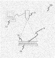
12 コンピュータ
14 ラインスキャン撮像装置
16 ソーラウェーハ
18 赤外線光源
20 微小割れ
22 画像解像度
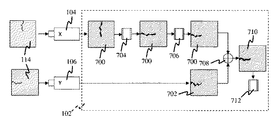
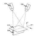
100 装置
102 コンピュータ
104 第1の撮像装置
106 第2の撮像装置
107 第1の方向
108、110 光源
109 第2の方向
112 搬送システム
114 ソーラウェーハ
116 第1の部分
118 第2の部分
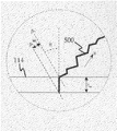
500、800 微小割れ
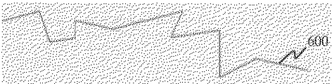
600 第1のビュー
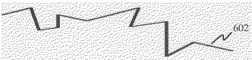
602 第2のビュー
604 第3のビュー
700 第1の画像
702 第2の画像
704 第1のプロセス
706 第2のプロセス
708 第3のプロセス
710 処理済み最終画像
712 第4のプロセス
900ミラー
Claims (24)
- ウェーハは内部に形成された割れを有し、第1の画像は前記割れの少なくとも1つの部分を含み、そこから第1の表面の前記第1の画像を得るため、第1の軸に略沿って前記ウェーハの前記第1の表面から出る光を受けることと、
第2の画像は前記割れの少なくとも1つの第2の部分を含み、前記第1の表面は平面に対して略平行に延び、前記平面上の前記第1の軸の正投影は、前記平面上の第2の軸の正投影に略直交し、そこから前記第1の表面の前記第2の画像を得るため、前記第2の軸に略沿って前記ウェーハの前記第1の表面から出る光を受けることと、
前記第1および第2の画像のそれぞれの前記割れの前記少なくとも1つの第1の部分および前記割れの前記少なくとも1つの第2の部分から、第3の画像を構築することと、を含み、
前記第3の画像は前記ウェーハの前記割れを検査するように実質的に処理可能である、検査方法。 - 光を前記第1の軸に略沿って前記ウェーハの第2の表面に向けて、それにより、前記ウェーハの前記第1の表面から前記第1の軸に沿って出る前記光を得ることと、光を前記第2の軸に略沿って前記ウェーハの第2の表面に向けて、それにより、前記ウェーハの前記第1の表面から前記第2の軸に沿って出る光を得ることとをさらに含み、前記第1の表面は前記第2の表面に略外側に向けて対向する、請求項1に記載の検査方法。
- 光を前記第1の表面に対して略鋭角で前記ウェーハの前記第1の表面に向けることをさらに含む、請求項1に記載の検査方法。
- 前記第1の画像および前記第2の画像から第3の画像を構築することには、前記第1の画像および前記第2の画像を重ね合わせて前記第3の画像を得ることが含まれる、請求項1に記載の検査方法。
- 前記第1の軸に略沿って前記ウェーハの前記第1の表面から出る光を受けて、そこから前記第1の表面の前記第1の画像を得ることには、前記ウェーハの前記第2の表面から前記第2の表面に対して鋭角で光を受けることが含まれる、請求項1に記載の検査方法。
- 前記ウェーハの前記第1の表面から受けた光を前記平面上の前記第1の軸の前記正投影に沿って向けるための光学ユニットを設けることをさらに含む、請求項1に記載の検査方法。
- 前記第2の軸に略沿って前記ウェーハの前記第1の表面から出る光を受けて、そこから前記第1の表面の前記第2の画像を得ることには、前記第1の表面に対して略直角で前記ウェーハの前記第1の表面からの光を受けることが含まれる、請求項1に記載の検査方法。
- 前記第1の軸に略沿って前記ウェーハの前記第1の表面から出る光を受けて、そこから前記第1の表面の前記第1の画像を得ることには、前記平面上の前記第1の軸の前記正投影に沿って前記ウェーハを搬送することが含まれる、請求項1に記載の検査方法。
- 前記第2の軸に略沿って前記ウェーハの前記第1の表面から出る光を受けて、そこから前記第1の表面の前記第2の画像を得ることには、前記平面上の前記第2の軸の前記正投影に沿って前記ウェーハを搬送することが含まれる、請求項1に記載の検査方法。
- 前記第2の軸に略沿って前記ウェーハの前記第1の表面から出る光を受けて、そこから前記第1の表面の前記第2の画像を得ることには、少なくとも前記第1および第2の画像を回転させて、前記第1の画像を前記第2の画像に空間的に見当合わせをすることが含まれる、請求項1に記載の検査方法。
- 前記第2の軸に略沿って前記ウェーハの前記第1の表面から出る光を受けて、そこから前記第1の表面の前記第2の画像を得ることには、前記第1の画像と前記第2の画像との視点およびスカラー差を補正することが含まれる、請求項1に記載の検査方法。
- 前記第1および第2の画像から第3の画像を構築することには、算術関数によって前記第1および第2の画像を組み合わせることが含まれる、請求項1に記載の検査方法。
- 前記算術関数によって前記第1および第2の画像を組み合わせることには、最小関数によって前記第3の画像を得ることが含まれる、請求項12に記載の検査方法。
- 光を内部に形成された割れを有するウェーハの第1の表面に向けるように配置される光組立体と、
前記ウェーハの第2の表面から第1の軸に略沿って出る光を受けるように配置される第1の撮像装置であって、前記光から、前記割れの少なくとも1つの第1の部分を含む第1の画像を取得可能であり、前記第2の表面は、平面に対して略平行し、前記第1の表面に対して外側に向かって略対向する、第1の撮像装置と、
前記ウェーハの前記第2の表面から第2の軸に略沿って出る光を受けるように配置される第2の撮像装置であって、前記光から、前記割れの少なくとも1つの第2の部分を含む第2の画像を取得可能であり、前記第1および第2の撮像装置は、前記平面上の前記第1の軸の正投影を前記平面上の前記第2の軸の正投影に略直交するように配置するように相互に構成され、コンピュータにデータ結合可能であり、それにより、前記第1および第2の画像の取得を可能にする、第2の撮像装置と
を備え、
第3の画像が、前記コンピュータにより前記第1および第2の画像から構築可能であり、続けて前記ウェーハの前記割れを検査するために処理可能である、検査装置。 - 前記光は、前記ウェーハの前記第1の表面に向けられ、前記ウェーハの前記第2の表面に対して略鋭角で前記ウェーハの前記第2の表面から受けられる、請求項14に記載の検査装置。
- 前記ウェーハの前記第2の表面から受けた光を前記平面上の前記第1の軸の前記正投影に略平行な方向に沿って向けるための光学ユニットをさらに備える、請求項14に記載の検査装置。
- 前記ウェーハの前記第2の表面からの前記光は、前記第1および第2の撮像装置のうちの少なくとも一方によって前記第2の表面に対して略直角に受けられる、請求項14に記載の検査装置。
- 前記平面上の前記第1の軸の前記正投影に略平行な第1の方向に前記ウェーハを搬送するための第1の部分を有する搬送システムをさらに備える、請求項14に記載の検査装置。
- 前記搬送システムは、前記平面上の前記第2の軸の前記正投影に略平行な第2の方向に前記ウェーハを搬送するための第2の部分を有する、請求項18に記載の検査装置。
- 前記コンピュータは、前記第1および第2の画像のうちの少なくとも一方を回転させて、前記第1の画像を前記第2の画像に空間的に見当合わせをする、請求項14に記載の検査装置。
- 前記コンピュータは、前記第1の画像と前記第2の画像との視点およびスカラー差を補正する、請求項14に記載の検査装置。
- 前記コンピュータは、算術関数によって前記第1および第2の画像を構築する、請求項14に記載の検査装置。
- 前記第1および第2の画像は最小関数によって構築される、請求項22に記載の検査装置。
- 前記光組立体は、第1の光源および第2の光源のうちの少なくとも一方を備える、請求項14に記載の検査装置。
Applications Claiming Priority (2)
| Application Number | Priority Date | Filing Date | Title |
|---|---|---|---|
| SG200805811-7 | 2008-07-28 | ||
| SG200805811-7A SG158782A1 (en) | 2008-07-28 | 2008-07-28 | Method and system for detecting micro-cracks in wafers |
Publications (2)
| Publication Number | Publication Date |
|---|---|
| JP2010034524A true JP2010034524A (ja) | 2010-02-12 |
| JP5500414B2 JP5500414B2 (ja) | 2014-05-21 |
Family
ID=41610587
Family Applications (1)
| Application Number | Title | Priority Date | Filing Date |
|---|---|---|---|
| JP2009139963A Active JP5500414B2 (ja) | 2008-07-28 | 2009-06-11 | ウェーハの微小割れを検出する検査方法および検査装置 |
Country Status (10)
| Country | Link |
|---|---|
| US (1) | US9651502B2 (ja) |
| EP (1) | EP2316127B8 (ja) |
| JP (1) | JP5500414B2 (ja) |
| KR (1) | KR101584386B1 (ja) |
| CN (1) | CN102105972B (ja) |
| HU (1) | HUE042046T2 (ja) |
| MY (1) | MY153553A (ja) |
| SG (1) | SG158782A1 (ja) |
| TW (1) | TWI476399B (ja) |
| WO (1) | WO2010014041A1 (ja) |
Cited By (1)
| Publication number | Priority date | Publication date | Assignee | Title |
|---|---|---|---|---|
| JP2018137309A (ja) * | 2017-02-21 | 2018-08-30 | 株式会社ディスコ | ウエーハの加工方法 |
Families Citing this family (15)
| Publication number | Priority date | Publication date | Assignee | Title |
|---|---|---|---|---|
| JP5243785B2 (ja) * | 2007-12-28 | 2013-07-24 | 日清紡ホールディングス株式会社 | 太陽電池検査装置及び太陽電池欠陥判定方法 |
| SG158787A1 (en) | 2008-07-28 | 2010-02-26 | Chan Sok Leng | Apparatus for detecting micro-cracks in wafers and method therefor |
| US20100309309A1 (en) * | 2009-06-05 | 2010-12-09 | Shenzhen Siweier Detecting Technology Ltd. | Method for precisely detecting crack width |
| US9735036B2 (en) * | 2011-08-19 | 2017-08-15 | Cognex Corporation | System and method for aligning a wafer for fabrication |
| US9136185B2 (en) * | 2011-12-19 | 2015-09-15 | MEMC Singapore Pte., Ltd. | Methods and systems for grain size evaluation of multi-cystalline solar wafers |
| US11629951B2 (en) * | 2013-07-09 | 2023-04-18 | Auburn University | Determining geometric characteristics of reflective surfaces and transparent materials |
| JP6280365B2 (ja) * | 2013-12-27 | 2018-02-14 | 三星ダイヤモンド工業株式会社 | 薄膜太陽電池の加工溝検出方法および加工溝検出装置 |
| WO2016103007A1 (fr) * | 2014-12-24 | 2016-06-30 | Arcelormittal | Procédé de contrôle d'un support comprenant un substrat métallique, un revêtement diélectrique, et une couche conductrice |
| US10018565B2 (en) * | 2015-05-04 | 2018-07-10 | Semilab Semiconductor Physics Laboratory Co., Ltd. | Micro photoluminescence imaging with optical filtering |
| WO2017158744A1 (ja) * | 2016-03-16 | 2017-09-21 | 株式会社 日立ハイテクノロジーズ | 欠陥検査方法及び欠陥検査装置 |
| US10692204B2 (en) * | 2016-08-01 | 2020-06-23 | The Boeing Company | System and method for high speed surface and subsurface FOD and defect detection |
| WO2018048843A1 (en) * | 2016-09-08 | 2018-03-15 | Corning Incorporated | Optical inspection systems and methods for detecting surface defects in a transparent sheet |
| CN106530287A (zh) * | 2016-10-24 | 2017-03-22 | 武汉新芯集成电路制造有限公司 | 一种基于晶圆内部缺陷检测的图像自动识别系统 |
| TWI670469B (zh) * | 2018-08-24 | 2019-09-01 | 超能高新材料股份有限公司 | 一種晶體品質判定方法 |
| US12135296B2 (en) | 2022-04-29 | 2024-11-05 | Applied Materials, Inc. | Edge inspection of silicon wafers by image stacking |
Citations (2)
| Publication number | Priority date | Publication date | Assignee | Title |
|---|---|---|---|---|
| JP2004271269A (ja) * | 2003-03-06 | 2004-09-30 | Topcon Corp | パターン検査方法及びパターン検査装置 |
| JP2006184177A (ja) * | 2004-12-28 | 2006-07-13 | Mitsubishi Electric Corp | 赤外検査装置及び赤外検査方法 |
Family Cites Families (30)
| Publication number | Priority date | Publication date | Assignee | Title |
|---|---|---|---|---|
| US4689491A (en) * | 1985-04-19 | 1987-08-25 | Datasonics Corp. | Semiconductor wafer scanning system |
| JP3314440B2 (ja) | 1993-02-26 | 2002-08-12 | 株式会社日立製作所 | 欠陥検査装置およびその方法 |
| US20020054291A1 (en) * | 1997-06-27 | 2002-05-09 | Tsai Bin-Ming Benjamin | Inspection system simultaneously utilizing monochromatic darkfield and broadband brightfield illumination sources |
| US6088470A (en) * | 1998-01-27 | 2000-07-11 | Sensar, Inc. | Method and apparatus for removal of bright or dark spots by the fusion of multiple images |
| US7061601B2 (en) * | 1999-07-02 | 2006-06-13 | Kla-Tencor Technologies Corporation | System and method for double sided optical inspection of thin film disks or wafers |
| US6891570B2 (en) * | 2001-01-31 | 2005-05-10 | Itt Manufacturing Enterprises Inc. | Method and adaptively deriving exposure time and frame rate from image motion |
| JP2002310929A (ja) | 2001-04-13 | 2002-10-23 | Mitsubishi Electric Corp | 欠陥検査装置 |
| JP2003017536A (ja) | 2001-07-04 | 2003-01-17 | Nec Corp | パターン検査方法及び検査装置 |
| US6768543B1 (en) * | 2001-11-01 | 2004-07-27 | Arun Ananth Aiyer | Wafer inspection apparatus with unique illumination methodology and method of operation |
| JP2004317470A (ja) | 2003-04-11 | 2004-11-11 | Nippon Electro Sensari Device Kk | 透明板欠陥検査装置 |
| WO2005100961A2 (en) | 2004-04-19 | 2005-10-27 | Phoseon Technology, Inc. | Imaging semiconductor strucutures using solid state illumination |
| US7693324B2 (en) * | 2004-07-13 | 2010-04-06 | International Business Machines Corporation | Optical surface inspection |
| US7283224B1 (en) | 2004-09-30 | 2007-10-16 | Smithgall & Associates, Inc. | Face lighting for edge location in catalytic converter inspection |
| DE102004054102A1 (de) * | 2004-11-09 | 2006-05-11 | Dr. Schenk Gmbh Industriemesstechnik | Verfahren und Vorrichtung zur Untersuchung eines scheibenförmigen Datenträgers |
| JP2006351669A (ja) | 2005-06-14 | 2006-12-28 | Mitsubishi Electric Corp | 赤外検査装置および赤外検査方法ならびに半導体ウェハの製造方法 |
| US8064054B2 (en) | 2005-10-11 | 2011-11-22 | Bt Imaging Pty Ltd | Method and system for inspecting indirect bandgap semiconductor structure |
| JP4696856B2 (ja) * | 2005-11-02 | 2011-06-08 | オムロン株式会社 | 画像処理装置、画像処理方法、そのプログラム、およびそのプログラムを記録したコンピュータ読取り可能な記録媒体 |
| JP4892943B2 (ja) | 2005-11-30 | 2012-03-07 | 凸版印刷株式会社 | 濃度ムラ検査装置 |
| WO2007073879A1 (de) * | 2005-12-16 | 2007-07-05 | Automation W + R Gmbh | Verfahren und anornung zur erkennung von materialfehlern, in werkstücken |
| DE102005061785B4 (de) * | 2005-12-23 | 2008-04-03 | Basler Ag | Verfahren und Vorrichtung zum Erkennen von Rissen in Silizium-Wafern |
| US20070188610A1 (en) * | 2006-02-13 | 2007-08-16 | The Boeing Company | Synoptic broad-area remote-sensing via multiple telescopes |
| JP4575886B2 (ja) | 2006-02-14 | 2010-11-04 | シャープ株式会社 | 多結晶半導体ウエハの割れ検査装置および割れ検査方法 |
| US7567344B2 (en) | 2006-05-12 | 2009-07-28 | Corning Incorporated | Apparatus and method for characterizing defects in a transparent substrate |
| US7851722B2 (en) | 2006-06-15 | 2010-12-14 | Satake Corporation | Optical cracked-grain selector |
| JP4960161B2 (ja) | 2006-10-11 | 2012-06-27 | 日東電工株式会社 | 検査データ処理装置及び検査データ処理方法 |
| JP4065893B1 (ja) * | 2006-12-04 | 2008-03-26 | 東京エレクトロン株式会社 | 欠陥検出装置、欠陥検出方法、情報処理装置、情報処理方法及びそのプログラム |
| DE102007006525B4 (de) * | 2007-02-06 | 2009-05-14 | Basler Ag | Verfahren und Vorrichtung zur Detektierung von Defekten |
| JP2008267851A (ja) | 2007-04-17 | 2008-11-06 | Ushio Inc | パターン検査装置およびパターン検査方法 |
| EP2006804A1 (en) | 2007-06-22 | 2008-12-24 | Siemens Aktiengesellschaft | Method for optical inspection of a matt surface and apparatus for applying this method |
| SG158787A1 (en) | 2008-07-28 | 2010-02-26 | Chan Sok Leng | Apparatus for detecting micro-cracks in wafers and method therefor |
-
2008
- 2008-07-28 SG SG200805811-7A patent/SG158782A1/en unknown
-
2009
- 2009-05-14 CN CN2009801294423A patent/CN102105972B/zh active Active
- 2009-05-14 KR KR1020107025770A patent/KR101584386B1/ko active Active
- 2009-05-14 HU HUE09803217 patent/HUE042046T2/hu unknown
- 2009-05-14 WO PCT/SG2009/000173 patent/WO2010014041A1/en not_active Ceased
- 2009-05-14 MY MYPI2010006299A patent/MY153553A/en unknown
- 2009-05-14 EP EP09803217.0A patent/EP2316127B8/en active Active
- 2009-05-14 US US12/681,717 patent/US9651502B2/en active Active
- 2009-05-22 TW TW098117189A patent/TWI476399B/zh active
- 2009-06-11 JP JP2009139963A patent/JP5500414B2/ja active Active
Patent Citations (2)
| Publication number | Priority date | Publication date | Assignee | Title |
|---|---|---|---|---|
| JP2004271269A (ja) * | 2003-03-06 | 2004-09-30 | Topcon Corp | パターン検査方法及びパターン検査装置 |
| JP2006184177A (ja) * | 2004-12-28 | 2006-07-13 | Mitsubishi Electric Corp | 赤外検査装置及び赤外検査方法 |
Cited By (1)
| Publication number | Priority date | Publication date | Assignee | Title |
|---|---|---|---|---|
| JP2018137309A (ja) * | 2017-02-21 | 2018-08-30 | 株式会社ディスコ | ウエーハの加工方法 |
Also Published As
| Publication number | Publication date |
|---|---|
| EP2316127B8 (en) | 2018-10-31 |
| CN102105972B (zh) | 2012-10-03 |
| WO2010014041A1 (en) | 2010-02-04 |
| HUE042046T2 (hu) | 2019-10-28 |
| KR101584386B1 (ko) | 2016-01-13 |
| US20100220186A1 (en) | 2010-09-02 |
| MY153553A (en) | 2015-02-27 |
| EP2316127B1 (en) | 2018-08-29 |
| CN102105972A (zh) | 2011-06-22 |
| US9651502B2 (en) | 2017-05-16 |
| EP2316127A1 (en) | 2011-05-04 |
| SG158782A1 (en) | 2010-02-26 |
| TW201005283A (en) | 2010-02-01 |
| KR20110058742A (ko) | 2011-06-01 |
| JP5500414B2 (ja) | 2014-05-21 |
| TWI476399B (zh) | 2015-03-11 |
| EP2316127A4 (en) | 2013-12-04 |
Similar Documents
| Publication | Publication Date | Title |
|---|---|---|
| JP5500414B2 (ja) | ウェーハの微小割れを検出する検査方法および検査装置 | |
| US8428337B2 (en) | Apparatus for detecting micro-cracks in wafers and method therefor | |
| US20090196489A1 (en) | High resolution edge inspection | |
| JP5549985B2 (ja) | ウェーハの微小割れを検出するための装置およびそのための方法 | |
| JP5085953B2 (ja) | 表面検査装置 | |
| JP6752593B2 (ja) | 欠陥検査装置 | |
| US9255893B2 (en) | Apparatus for illuminating substrates in order to image micro cracks, pinholes and inclusions in monocrystalline and polycrystalline substrates and method therefore | |
| JP2012037425A (ja) | 多結晶シリコンウェーハの検査方法及びその装置 | |
| JPWO2009072483A1 (ja) | 観察装置および観察方法 | |
| CN108604880B (zh) | 检测太阳能晶片上的豁口的方法和系统 | |
| US8488867B2 (en) | Inspection device for disk-shaped substrate | |
| JP2022138855A (ja) | 半導体チップの検査方法及び装置 | |
| CN111855663B (zh) | 一种检测晶圆缺陷的设备和方法 | |
| JP4243268B2 (ja) | パターン検査装置、及びパターン検査方法 | |
| JP2009198395A (ja) | 表面検査装置 | |
| JP4613090B2 (ja) | 検査装置 | |
| JP2000206051A (ja) | 半導体検査装置 | |
| JP2001091473A (ja) | 基板検査装置 | |
| KR20080102502A (ko) | 반도체 기판의 결함 검출 방법 |
Legal Events
| Date | Code | Title | Description |
|---|---|---|---|
| A711 | Notification of change in applicant |
Free format text: JAPANESE INTERMEDIATE CODE: A711 Effective date: 20100413 |
|
| A521 | Request for written amendment filed |
Free format text: JAPANESE INTERMEDIATE CODE: A821 Effective date: 20100413 |
|
| A621 | Written request for application examination |
Free format text: JAPANESE INTERMEDIATE CODE: A621 Effective date: 20111003 |
|
| A521 | Request for written amendment filed |
Free format text: JAPANESE INTERMEDIATE CODE: A523 Effective date: 20121204 |
|
| A977 | Report on retrieval |
Free format text: JAPANESE INTERMEDIATE CODE: A971007 Effective date: 20130612 |
|
| A131 | Notification of reasons for refusal |
Free format text: JAPANESE INTERMEDIATE CODE: A131 Effective date: 20130618 |
|
| A601 | Written request for extension of time |
Free format text: JAPANESE INTERMEDIATE CODE: A601 Effective date: 20130917 |
|
| A602 | Written permission of extension of time |
Free format text: JAPANESE INTERMEDIATE CODE: A602 Effective date: 20131002 |
|
| A521 | Request for written amendment filed |
Free format text: JAPANESE INTERMEDIATE CODE: A523 Effective date: 20131016 |
|
| A131 | Notification of reasons for refusal |
Free format text: JAPANESE INTERMEDIATE CODE: A131 Effective date: 20131224 |
|
| A521 | Request for written amendment filed |
Free format text: JAPANESE INTERMEDIATE CODE: A523 Effective date: 20131226 |
|
| TRDD | Decision of grant or rejection written | ||
| A01 | Written decision to grant a patent or to grant a registration (utility model) |
Free format text: JAPANESE INTERMEDIATE CODE: A01 Effective date: 20140128 |
|
| A61 | First payment of annual fees (during grant procedure) |
Free format text: JAPANESE INTERMEDIATE CODE: A61 Effective date: 20140227 |
|
| R150 | Certificate of patent or registration of utility model |
Ref document number: 5500414 Country of ref document: JP Free format text: JAPANESE INTERMEDIATE CODE: R150 |
|
| R250 | Receipt of annual fees |
Free format text: JAPANESE INTERMEDIATE CODE: R250 |
|
| S111 | Request for change of ownership or part of ownership |
Free format text: JAPANESE INTERMEDIATE CODE: R313113 |
|
| S531 | Written request for registration of change of domicile |
Free format text: JAPANESE INTERMEDIATE CODE: R313531 |
|
| R350 | Written notification of registration of transfer |
Free format text: JAPANESE INTERMEDIATE CODE: R350 |
|
| R250 | Receipt of annual fees |
Free format text: JAPANESE INTERMEDIATE CODE: R250 |
|
| R250 | Receipt of annual fees |
Free format text: JAPANESE INTERMEDIATE CODE: R250 |
|
| R250 | Receipt of annual fees |
Free format text: JAPANESE INTERMEDIATE CODE: R250 |
|
| R250 | Receipt of annual fees |
Free format text: JAPANESE INTERMEDIATE CODE: R250 |
|
| R250 | Receipt of annual fees |
Free format text: JAPANESE INTERMEDIATE CODE: R250 |
|
| R250 | Receipt of annual fees |
Free format text: JAPANESE INTERMEDIATE CODE: R250 |
|
| R250 | Receipt of annual fees |
Free format text: JAPANESE INTERMEDIATE CODE: R250 |
|
| R250 | Receipt of annual fees |
Free format text: JAPANESE INTERMEDIATE CODE: R250 |