JP2010032659A - 波長選択フィルタ、フィルタ装置、光源装置、光学装置及び屈折率センサ - Google Patents
波長選択フィルタ、フィルタ装置、光源装置、光学装置及び屈折率センサ Download PDFInfo
- Publication number
- JP2010032659A JP2010032659A JP2008192942A JP2008192942A JP2010032659A JP 2010032659 A JP2010032659 A JP 2010032659A JP 2008192942 A JP2008192942 A JP 2008192942A JP 2008192942 A JP2008192942 A JP 2008192942A JP 2010032659 A JP2010032659 A JP 2010032659A
- Authority
- JP
- Japan
- Prior art keywords
- wavelength
- light
- refractive index
- layer
- light source
- Prior art date
- Legal status (The legal status is an assumption and is not a legal conclusion. Google has not performed a legal analysis and makes no representation as to the accuracy of the status listed.)
- Granted
Links
- 230000003287 optical effect Effects 0.000 title claims description 63
- 239000000758 substrate Substances 0.000 claims abstract description 39
- 230000007246 mechanism Effects 0.000 claims description 15
- 238000001514 detection method Methods 0.000 claims description 7
- 230000001788 irregular Effects 0.000 abstract 2
- 238000010586 diagram Methods 0.000 description 18
- 230000008878 coupling Effects 0.000 description 14
- 238000010168 coupling process Methods 0.000 description 14
- 238000005859 coupling reaction Methods 0.000 description 14
- 238000004519 manufacturing process Methods 0.000 description 12
- 239000000463 material Substances 0.000 description 9
- 229920002120 photoresistant polymer Polymers 0.000 description 9
- 238000005229 chemical vapour deposition Methods 0.000 description 8
- 238000001312 dry etching Methods 0.000 description 8
- 238000005240 physical vapour deposition Methods 0.000 description 8
- 230000000052 comparative effect Effects 0.000 description 7
- 238000005530 etching Methods 0.000 description 6
- 238000000034 method Methods 0.000 description 6
- 230000008859 change Effects 0.000 description 5
- VYPSYNLAJGMNEJ-UHFFFAOYSA-N Silicium dioxide Chemical compound O=[Si]=O VYPSYNLAJGMNEJ-UHFFFAOYSA-N 0.000 description 3
- 238000001914 filtration Methods 0.000 description 3
- 239000012780 transparent material Substances 0.000 description 3
- CSCPPACGZOOCGX-UHFFFAOYSA-N Acetone Chemical compound CC(C)=O CSCPPACGZOOCGX-UHFFFAOYSA-N 0.000 description 2
- 238000004458 analytical method Methods 0.000 description 2
- 238000013461 design Methods 0.000 description 2
- 238000001020 plasma etching Methods 0.000 description 2
- 230000008569 process Effects 0.000 description 2
- 229910018072 Al 2 O 3 Inorganic materials 0.000 description 1
- GWEVSGVZZGPLCZ-UHFFFAOYSA-N Titan oxide Chemical compound O=[Ti]=O GWEVSGVZZGPLCZ-UHFFFAOYSA-N 0.000 description 1
- QVGXLLKOCUKJST-UHFFFAOYSA-N atomic oxygen Chemical compound [O] QVGXLLKOCUKJST-UHFFFAOYSA-N 0.000 description 1
- 238000004364 calculation method Methods 0.000 description 1
- 238000000354 decomposition reaction Methods 0.000 description 1
- 238000007598 dipping method Methods 0.000 description 1
- 235000012489 doughnuts Nutrition 0.000 description 1
- 238000010828 elution Methods 0.000 description 1
- 238000007689 inspection Methods 0.000 description 1
- 238000010884 ion-beam technique Methods 0.000 description 1
- 239000007788 liquid Substances 0.000 description 1
- 238000005259 measurement Methods 0.000 description 1
- 238000012986 modification Methods 0.000 description 1
- 230000004048 modification Effects 0.000 description 1
- ZKATWMILCYLAPD-UHFFFAOYSA-N niobium pentoxide Inorganic materials O=[Nb](=O)O[Nb](=O)=O ZKATWMILCYLAPD-UHFFFAOYSA-N 0.000 description 1
- URLJKFSTXLNXLG-UHFFFAOYSA-N niobium(5+);oxygen(2-) Chemical compound [O-2].[O-2].[O-2].[O-2].[O-2].[Nb+5].[Nb+5] URLJKFSTXLNXLG-UHFFFAOYSA-N 0.000 description 1
- 239000003960 organic solvent Substances 0.000 description 1
- TWNQGVIAIRXVLR-UHFFFAOYSA-N oxo(oxoalumanyloxy)alumane Chemical compound O=[Al]O[Al]=O TWNQGVIAIRXVLR-UHFFFAOYSA-N 0.000 description 1
- 229910052760 oxygen Inorganic materials 0.000 description 1
- 239000001301 oxygen Substances 0.000 description 1
- BPUBBGLMJRNUCC-UHFFFAOYSA-N oxygen(2-);tantalum(5+) Chemical compound [O-2].[O-2].[O-2].[O-2].[O-2].[Ta+5].[Ta+5] BPUBBGLMJRNUCC-UHFFFAOYSA-N 0.000 description 1
- 230000002093 peripheral effect Effects 0.000 description 1
- 238000012805 post-processing Methods 0.000 description 1
- 239000002994 raw material Substances 0.000 description 1
- 238000001448 refractive index detection Methods 0.000 description 1
- 238000004528 spin coating Methods 0.000 description 1
- 239000000126 substance Substances 0.000 description 1
- PBCFLUZVCVVTBY-UHFFFAOYSA-N tantalum pentoxide Inorganic materials O=[Ta](=O)O[Ta](=O)=O PBCFLUZVCVVTBY-UHFFFAOYSA-N 0.000 description 1
Images


Classifications
-
- G—PHYSICS
- G02—OPTICS
- G02B—OPTICAL ELEMENTS, SYSTEMS OR APPARATUS
- G02B5/00—Optical elements other than lenses
- G02B5/18—Diffraction gratings
- G02B5/1847—Manufacturing methods
- G02B5/1857—Manufacturing methods using exposure or etching means, e.g. holography, photolithography, exposure to electron or ion beams
-
- G—PHYSICS
- G02—OPTICS
- G02B—OPTICAL ELEMENTS, SYSTEMS OR APPARATUS
- G02B5/00—Optical elements other than lenses
- G02B5/18—Diffraction gratings
- G02B5/1861—Reflection gratings characterised by their structure, e.g. step profile, contours of substrate or grooves, pitch variations, materials
-
- G—PHYSICS
- G01—MEASURING; TESTING
- G01N—INVESTIGATING OR ANALYSING MATERIALS BY DETERMINING THEIR CHEMICAL OR PHYSICAL PROPERTIES
- G01N21/00—Investigating or analysing materials by the use of optical means, i.e. using sub-millimetre waves, infrared, visible or ultraviolet light
- G01N21/75—Systems in which material is subjected to a chemical reaction, the progress or the result of the reaction being investigated
- G01N21/77—Systems in which material is subjected to a chemical reaction, the progress or the result of the reaction being investigated by observing the effect on a chemical indicator
- G01N2021/7769—Measurement method of reaction-produced change in sensor
- G01N2021/7773—Reflection
-
- G—PHYSICS
- G02—OPTICS
- G02B—OPTICAL ELEMENTS, SYSTEMS OR APPARATUS
- G02B7/00—Mountings, adjusting means, or light-tight connections, for optical elements
- G02B7/003—Alignment of optical elements
Abstract
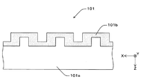
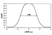
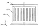
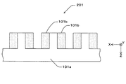
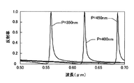
【解決手段】入射光が入射する面に形成され、X軸方向に関して矩形波形状の凹凸構造部を有する基板101aと、該凹凸構造部を覆う透明膜101bとを有し、透明膜101bの屈折率は、基板101aの屈折率よりも大きい。また、各凸部の+X側に隣接する透明膜101bと、各凸部の−X側に隣接する透明膜101bとの間に空気の層を有している。この場合には、波長選択性が高く、かつ光の入射角の許容範囲を従来よりも広くすることが可能となる。
【選択図】図7
Description
Claims (11)
- 入射光に含まれる特定波長の光を選択的に共鳴反射する波長選択フィルタであって、
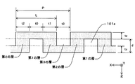
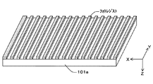
前記入射光が入射する面に形成され、一の軸方向に関して矩形波形状の凹凸構造部を有する基板と;
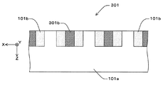
前記一の軸方向に関して、前記凹凸構造部における各凸部の一側の面を覆う第1の層と、前記各凸部の他側の面を覆う第2の層とを含む多層構造体と;を有し、
前記第1の層の屈折率及び前記第2の層の屈折率は、いずれも前記基板の屈折率よりも大きいことを特徴とする波長選択フィルタ。 - 前記第1の層の屈折率と前記第2の層の屈折率は等しいことを特徴とする請求項1に記載の波長選択フィルタ。
- 前記多層構造体は、前記一の軸方向に関して、前記第1の層と前記第2の層との間に位置する第3の層を有し、
前記第3の層の屈折率は、前記基板の屈折率よりも小さいことを特徴とする請求項1又は2に記載の波長選択フィルタ。 - 前記第3の層は、空気の層であることを特徴とする請求項3に記載の波長選択フィルタ。
- 前記一の軸方向に関して、前記凹凸構造部における凸部の幅、前記第1の層の幅、前記第2の層の幅、及び前記第3の層の幅は、いずれも互いに等しいことを特徴とする請求項3又は4に記載の波長選択フィルタ。
- 前記凹凸構造部における凸部の高さは、該凸部の前記一の軸方向に関する幅の2倍であることを特徴とする請求項5に記載の波長選択フィルタ。
- 請求項1〜6のいずれか一項に記載の波長選択フィルタと;
前記波長選択フィルタを、前記基板の表面に平行で前記一の軸方向に直交する軸まわりに回動させる回動機構と;を備えるフィルタ装置。 - 光源と;
前記光源からの光束を略平行光とする光学素子と;
前記光学素子を介した光束が入射される請求項1〜6のいずれか一項に記載の波長選択フィルタと;を備え、
前記波長選択フィルタで反射された光束を出力することを特徴とする光源装置。 - 光源と;
前記光源からの光束を略平行光とする光学素子と;
前記光学素子を介した光束が入射される請求項7に記載のフィルタ装置と;を備え、
前記フィルタ装置の波長選択フィルタで反射された光束を出力することを特徴とする光源装置。 - 請求項8又は9に記載の光源装置と;
前記光源装置から出力された光束が入射される光学系と;を備える光学装置。 - 対象物の屈折率を検出するための屈折率センサであって、
光源と;
前記光源からの光束を略平行光とする第1の光学素子と;
前記第1の光学素子を介した光束を直線偏光とする第2の光学素子と;
前記第2の光学素子から射出され、対象物を透過した光束が入射される請求項1〜6のいずれか一項に記載の波長選択フィルタと;
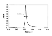
前記波長選択フィルタで反射された光束のピーク波長を求め、該ピーク波長に基づいて前記対象物の屈折率を検出する検出装置と;を備える屈折率センサ。
Priority Applications (3)
| Application Number | Priority Date | Filing Date | Title |
|---|---|---|---|
| JP2008192942A JP5256906B2 (ja) | 2008-07-28 | 2008-07-28 | 波長選択フィルタ、フィルタ装置、光源装置、光学装置及び屈折率センサ |
| EP09251885A EP2149802B1 (en) | 2008-07-28 | 2009-07-27 | Wavelength selection filter, filter unit, light source device, optical apparatus, and refractive index sensor |
| US12/510,448 US8213083B2 (en) | 2008-07-28 | 2009-07-28 | Wavelength selection filter, filter unit, light source device, optical apparatus, and refractive index sensor |
Applications Claiming Priority (1)
| Application Number | Priority Date | Filing Date | Title |
|---|---|---|---|
| JP2008192942A JP5256906B2 (ja) | 2008-07-28 | 2008-07-28 | 波長選択フィルタ、フィルタ装置、光源装置、光学装置及び屈折率センサ |
Publications (2)
| Publication Number | Publication Date |
|---|---|
| JP2010032659A true JP2010032659A (ja) | 2010-02-12 |
| JP5256906B2 JP5256906B2 (ja) | 2013-08-07 |
Family
ID=41078268
Family Applications (1)
| Application Number | Title | Priority Date | Filing Date |
|---|---|---|---|
| JP2008192942A Expired - Fee Related JP5256906B2 (ja) | 2008-07-28 | 2008-07-28 | 波長選択フィルタ、フィルタ装置、光源装置、光学装置及び屈折率センサ |
Country Status (3)
| Country | Link |
|---|---|
| US (1) | US8213083B2 (ja) |
| EP (1) | EP2149802B1 (ja) |
| JP (1) | JP5256906B2 (ja) |
Cited By (3)
| Publication number | Priority date | Publication date | Assignee | Title |
|---|---|---|---|---|
| JP2012073623A (ja) * | 2010-03-02 | 2012-04-12 | Sony Corp | 光学体、窓材、建具および日射遮蔽装置 |
| JP2015040910A (ja) * | 2013-08-20 | 2015-03-02 | 株式会社アスカネット | 対向する壁面への選択的蒸着方法 |
| JP2016046290A (ja) * | 2014-08-20 | 2016-04-04 | 日本板硝子株式会社 | 外部共振器型半導体レーザ用回折格子 |
Families Citing this family (7)
| Publication number | Priority date | Publication date | Assignee | Title |
|---|---|---|---|---|
| EP2352042B1 (en) * | 2010-01-29 | 2017-05-17 | Dexerials Corporation | Optical element and method for manufacturing the same |
| JP2013031054A (ja) | 2011-07-29 | 2013-02-07 | Ricoh Co Ltd | 撮像装置及びこれを備えた物体検出装置、並びに、光学フィルタ及びその製造方法 |
| JP2013029451A (ja) | 2011-07-29 | 2013-02-07 | Ricoh Co Ltd | 付着物検出装置及び付着物検出方法 |
| CN105022108B (zh) * | 2015-07-17 | 2017-07-14 | 中国科学院长春光学精密机械与物理研究所 | 双向轻量化高刚度双面分光镜 |
| KR101811515B1 (ko) * | 2016-01-22 | 2017-12-22 | 주식회사 케이씨씨 | 내장부품용 하이그로시 도료 조성물 |
| JP6748150B2 (ja) * | 2018-06-14 | 2020-08-26 | ファナック株式会社 | ガルバノミラー及びレーザ加工装置 |
| KR101997862B1 (ko) * | 2018-12-26 | 2019-07-08 | 제이피아이헬스케어 주식회사 | 격자형 x선 그리드 제조 방법 |
Citations (11)
| Publication number | Priority date | Publication date | Assignee | Title |
|---|---|---|---|---|
| JPS62269104A (ja) * | 1986-05-16 | 1987-11-21 | Nec Corp | 波長板 |
| JPH10142525A (ja) * | 1996-11-11 | 1998-05-29 | Fujikura Ltd | 光出力調整器 |
| JPH1123894A (ja) * | 1997-06-30 | 1999-01-29 | Oki Electric Ind Co Ltd | 光通信端末局用光学装置 |
| JP2001021711A (ja) * | 1999-07-12 | 2001-01-26 | Teijin Seiki Co Ltd | 波長選択フィルタの選択波長調整方法、波長多重化装置、光通信システム及び屈折率検知装置 |
| JP2002098820A (ja) * | 2000-09-21 | 2002-04-05 | Nippon Sheet Glass Co Ltd | 反射型回折格子 |
| JP2002258034A (ja) * | 2001-03-05 | 2002-09-11 | Japan Science & Technology Corp | 波長フィルタ |
| JP2003514250A (ja) * | 1999-09-17 | 2003-04-15 | ユーティ―バテル エルエルシー | 共振格子フィルタを用いた光マルチプレクサ/デマルチプレクサ |
| WO2005036218A1 (ja) * | 2003-10-07 | 2005-04-21 | Nalux Co., Ltd. | 偏光素子および偏光素子を含む光学系 |
| JP2006350126A (ja) * | 2005-06-17 | 2006-12-28 | Sharp Corp | 波長選択素子 |
| JP2008070867A (ja) * | 2006-07-28 | 2008-03-27 | Csem Centre Suisse D'electronique & De Microtechnique Sa | ゼロ次回折フィルタ |
| JP2009092569A (ja) * | 2007-10-10 | 2009-04-30 | Shimadzu Corp | 屈折率計 |
Family Cites Families (14)
| Publication number | Priority date | Publication date | Assignee | Title |
|---|---|---|---|---|
| JPS58198007A (ja) * | 1982-05-14 | 1983-11-17 | Ricoh Co Ltd | 保護膜を有する回折格子 |
| JPH04211202A (ja) * | 1990-03-19 | 1992-08-03 | Canon Inc | 反射型回折格子および該回折格子を用いた装置 |
| DE4303975A1 (de) * | 1993-02-11 | 1994-08-18 | Heidenhain Gmbh Dr Johannes | Teilungsträger |
| US6002522A (en) * | 1996-06-11 | 1999-12-14 | Kabushiki Kaisha Toshiba | Optical functional element comprising photonic crystal |
| US6035089A (en) * | 1997-06-11 | 2000-03-07 | Lockheed Martin Energy Research Corporation | Integrated narrowband optical filter based on embedded subwavelength resonant grating structures |
| JP4359713B2 (ja) * | 2000-11-24 | 2009-11-04 | コニカミノルタホールディングス株式会社 | 回折光学素子 |
| JP2005275092A (ja) | 2004-03-25 | 2005-10-06 | Nippon Zeon Co Ltd | 偏光分離素子 |
| JP2005275089A (ja) | 2004-03-25 | 2005-10-06 | Osaka Industrial Promotion Organization | チューナブル波長選択フィルタ |
| WO2006025980A2 (en) * | 2004-07-26 | 2006-03-09 | Applied Opsec, Inc. | Diffraction-based optical grating structure and method of creating the same |
| JP2006178312A (ja) * | 2004-12-24 | 2006-07-06 | Canon Inc | 表面反射型位相格子 |
| JP2006349776A (ja) * | 2005-06-13 | 2006-12-28 | Sharp Corp | 波長選択素子 |
| JP2007232456A (ja) | 2006-02-28 | 2007-09-13 | Canon Inc | 光学素子、屈折率センサ、および化学センサ |
| EP1862827B2 (en) * | 2006-05-31 | 2012-05-30 | CSEM Centre Suisse d'Electronique et de Microtechnique SA - Recherche et Développement | Nano-structured Zero-order diffractive filter |
| JP2008008990A (ja) | 2006-06-27 | 2008-01-17 | Ricoh Co Ltd | 波長板、画像投射装置、及び光ピックアップ装置 |
-
2008
- 2008-07-28 JP JP2008192942A patent/JP5256906B2/ja not_active Expired - Fee Related
-
2009
- 2009-07-27 EP EP09251885A patent/EP2149802B1/en active Active
- 2009-07-28 US US12/510,448 patent/US8213083B2/en not_active Expired - Fee Related
Patent Citations (11)
| Publication number | Priority date | Publication date | Assignee | Title |
|---|---|---|---|---|
| JPS62269104A (ja) * | 1986-05-16 | 1987-11-21 | Nec Corp | 波長板 |
| JPH10142525A (ja) * | 1996-11-11 | 1998-05-29 | Fujikura Ltd | 光出力調整器 |
| JPH1123894A (ja) * | 1997-06-30 | 1999-01-29 | Oki Electric Ind Co Ltd | 光通信端末局用光学装置 |
| JP2001021711A (ja) * | 1999-07-12 | 2001-01-26 | Teijin Seiki Co Ltd | 波長選択フィルタの選択波長調整方法、波長多重化装置、光通信システム及び屈折率検知装置 |
| JP2003514250A (ja) * | 1999-09-17 | 2003-04-15 | ユーティ―バテル エルエルシー | 共振格子フィルタを用いた光マルチプレクサ/デマルチプレクサ |
| JP2002098820A (ja) * | 2000-09-21 | 2002-04-05 | Nippon Sheet Glass Co Ltd | 反射型回折格子 |
| JP2002258034A (ja) * | 2001-03-05 | 2002-09-11 | Japan Science & Technology Corp | 波長フィルタ |
| WO2005036218A1 (ja) * | 2003-10-07 | 2005-04-21 | Nalux Co., Ltd. | 偏光素子および偏光素子を含む光学系 |
| JP2006350126A (ja) * | 2005-06-17 | 2006-12-28 | Sharp Corp | 波長選択素子 |
| JP2008070867A (ja) * | 2006-07-28 | 2008-03-27 | Csem Centre Suisse D'electronique & De Microtechnique Sa | ゼロ次回折フィルタ |
| JP2009092569A (ja) * | 2007-10-10 | 2009-04-30 | Shimadzu Corp | 屈折率計 |
Non-Patent Citations (1)
| Title |
|---|
| JPN6012044067; L.Mashev and E. Popov: 'ZERO ORDER ANOMALY OF DIELECTRIC COATED GRATINGS' OPTICS COMMUNICATIONS No.6/Vol.55, 19851015, 377-380, North-Holland Pub. Co. * |
Cited By (3)
| Publication number | Priority date | Publication date | Assignee | Title |
|---|---|---|---|---|
| JP2012073623A (ja) * | 2010-03-02 | 2012-04-12 | Sony Corp | 光学体、窓材、建具および日射遮蔽装置 |
| JP2015040910A (ja) * | 2013-08-20 | 2015-03-02 | 株式会社アスカネット | 対向する壁面への選択的蒸着方法 |
| JP2016046290A (ja) * | 2014-08-20 | 2016-04-04 | 日本板硝子株式会社 | 外部共振器型半導体レーザ用回折格子 |
Also Published As
| Publication number | Publication date |
|---|---|
| US8213083B2 (en) | 2012-07-03 |
| EP2149802B1 (en) | 2013-02-27 |
| JP5256906B2 (ja) | 2013-08-07 |
| US20100020401A1 (en) | 2010-01-28 |
| EP2149802A1 (en) | 2010-02-03 |
Similar Documents
| Publication | Publication Date | Title |
|---|---|---|
| JP5256906B2 (ja) | 波長選択フィルタ、フィルタ装置、光源装置、光学装置及び屈折率センサ | |
| KR102363805B1 (ko) | 파장이하 해상도 촬영을 위한 메타렌즈 | |
| US7408712B2 (en) | Polarization-selectively blazed, diffractive optical element | |
| JP5043167B2 (ja) | 反射型光電式エンコーダ用スケール及び光電式エンコーダ | |
| US7688512B2 (en) | Transmissive diffraction grating, and spectral separation element and spectroscope using the same | |
| JP5280654B2 (ja) | 透過型回折格子、並びに、それを用いた分光素子及び分光器 | |
| JP5876076B2 (ja) | 共鳴格子を有し、入射角に従って調整可能な偏光無依存型光フィルタ | |
| JP2006003447A (ja) | 偏光分離素子及びその製造方法 | |
| JP5739224B2 (ja) | 光学部品の製造方法及び光学部品 | |
| US7929209B2 (en) | Optical element and method of manufacturing optical element with each of first and second layers having a repetition structure | |
| CN110140089A (zh) | 结构的显微光刻制造 | |
| JP2010008990A (ja) | 光学フィルタ | |
| JP4913345B2 (ja) | 反射型光電式エンコーダ用スケール、スケールの製造方法及び光電式エンコーダ | |
| KR20140082855A (ko) | 빛 파면의 제어 | |
| JP6425875B2 (ja) | 光電式測定器用スケール、エンコーダ及びスケールの形成方法 | |
| JP5050922B2 (ja) | ファブリペロー干渉計 | |
| WO2022150816A1 (en) | Self-aligned nano-pillar coatings and method of manufacturing | |
| JP4294239B2 (ja) | レーザ加工装置および透過型の1/2波長板 | |
| JP2007333826A (ja) | 反射型回折素子 | |
| JP2007101926A (ja) | 透過型回折格子、ならびにそれを用いた分光素子および分光器 | |
| JP2010186147A (ja) | 赤外線光学フィルタおよびその製造方法 | |
| JP2007279458A (ja) | サブ波長格子光学素子 | |
| JP7325122B2 (ja) | 光吸収素子、光吸収体、及び光吸収素子の製造方法 | |
| Lee et al. | Blazed binary diffractive gratings with antireflection coating for improved operation at 10.6 μm | |
| JP4415756B2 (ja) | 光学素子並びにその製造方法 |
Legal Events
| Date | Code | Title | Description |
|---|---|---|---|
| A621 | Written request for application examination |
Free format text: JAPANESE INTERMEDIATE CODE: A621 Effective date: 20110408 |
|
| A977 | Report on retrieval |
Free format text: JAPANESE INTERMEDIATE CODE: A971007 Effective date: 20120625 |
|
| A131 | Notification of reasons for refusal |
Free format text: JAPANESE INTERMEDIATE CODE: A131 Effective date: 20120827 |
|
| A521 | Request for written amendment filed |
Free format text: JAPANESE INTERMEDIATE CODE: A523 Effective date: 20121004 |
|
| TRDD | Decision of grant or rejection written | ||
| A01 | Written decision to grant a patent or to grant a registration (utility model) |
Free format text: JAPANESE INTERMEDIATE CODE: A01 Effective date: 20130326 |
|
| A61 | First payment of annual fees (during grant procedure) |
Free format text: JAPANESE INTERMEDIATE CODE: A61 Effective date: 20130408 |
|
| FPAY | Renewal fee payment (event date is renewal date of database) |
Free format text: PAYMENT UNTIL: 20160502 Year of fee payment: 3 |
|
| R151 | Written notification of patent or utility model registration |
Ref document number: 5256906 Country of ref document: JP Free format text: JAPANESE INTERMEDIATE CODE: R151 |
|
| LAPS | Cancellation because of no payment of annual fees |