JP2010026069A - 振動ミラー素子 - Google Patents
振動ミラー素子 Download PDFInfo
- Publication number
- JP2010026069A JP2010026069A JP2008184913A JP2008184913A JP2010026069A JP 2010026069 A JP2010026069 A JP 2010026069A JP 2008184913 A JP2008184913 A JP 2008184913A JP 2008184913 A JP2008184913 A JP 2008184913A JP 2010026069 A JP2010026069 A JP 2010026069A
- Authority
- JP
- Japan
- Prior art keywords
- substrate
- mirror
- piezoelectric
- base member
- mirror element
- Prior art date
- Legal status (The legal status is an assumption and is not a legal conclusion. Google has not performed a legal analysis and makes no representation as to the accuracy of the status listed.)
- Granted
Links
Images


Classifications
-
- G—PHYSICS
- G02—OPTICS
- G02B—OPTICAL ELEMENTS, SYSTEMS OR APPARATUS
- G02B26/00—Optical devices or arrangements for the control of light using movable or deformable optical elements
- G02B26/08—Optical devices or arrangements for the control of light using movable or deformable optical elements for controlling the direction of light
- G02B26/0816—Optical devices or arrangements for the control of light using movable or deformable optical elements for controlling the direction of light by means of one or more reflecting elements
- G02B26/0833—Optical devices or arrangements for the control of light using movable or deformable optical elements for controlling the direction of light by means of one or more reflecting elements the reflecting element being a micromechanical device, e.g. a MEMS mirror, DMD
- G02B26/0858—Optical devices or arrangements for the control of light using movable or deformable optical elements for controlling the direction of light by means of one or more reflecting elements the reflecting element being a micromechanical device, e.g. a MEMS mirror, DMD the reflecting means being moved or deformed by piezoelectric means
-
- B—PERFORMING OPERATIONS; TRANSPORTING
- B81—MICROSTRUCTURAL TECHNOLOGY
- B81B—MICROSTRUCTURAL DEVICES OR SYSTEMS, e.g. MICROMECHANICAL DEVICES
- B81B3/00—Devices comprising flexible or deformable elements, e.g. comprising elastic tongues or membranes
- B81B3/0035—Constitution or structural means for controlling the movement of the flexible or deformable elements
- B81B3/004—Angular deflection
-
- G—PHYSICS
- G02—OPTICS
- G02B—OPTICAL ELEMENTS, SYSTEMS OR APPARATUS
- G02B26/00—Optical devices or arrangements for the control of light using movable or deformable optical elements
- G02B26/08—Optical devices or arrangements for the control of light using movable or deformable optical elements for controlling the direction of light
- G02B26/10—Scanning systems
- G02B26/101—Scanning systems with both horizontal and vertical deflecting means, e.g. raster or XY scanners
-
- H—ELECTRICITY
- H04—ELECTRIC COMMUNICATION TECHNIQUE
- H04N—PICTORIAL COMMUNICATION, e.g. TELEVISION
- H04N1/00—Scanning, transmission or reproduction of documents or the like, e.g. facsimile transmission; Details thereof
- H04N1/04—Scanning arrangements, i.e. arrangements for the displacement of active reading or reproducing elements relative to the original or reproducing medium, or vice versa
- H04N1/10—Scanning arrangements, i.e. arrangements for the displacement of active reading or reproducing elements relative to the original or reproducing medium, or vice versa using flat picture-bearing surfaces
- H04N1/1013—Scanning arrangements, i.e. arrangements for the displacement of active reading or reproducing elements relative to the original or reproducing medium, or vice versa using flat picture-bearing surfaces with sub-scanning by translatory movement of at least a part of the main-scanning components
- H04N1/1017—Scanning arrangements, i.e. arrangements for the displacement of active reading or reproducing elements relative to the original or reproducing medium, or vice versa using flat picture-bearing surfaces with sub-scanning by translatory movement of at least a part of the main-scanning components the main-scanning components remaining positionally invariant with respect to one another in the sub-scanning direction
-
- B—PERFORMING OPERATIONS; TRANSPORTING
- B81—MICROSTRUCTURAL TECHNOLOGY
- B81B—MICROSTRUCTURAL DEVICES OR SYSTEMS, e.g. MICROMECHANICAL DEVICES
- B81B2201/00—Specific applications of microelectromechanical systems
- B81B2201/04—Optical MEMS
- B81B2201/042—Micromirrors, not used as optical switches
-
- B—PERFORMING OPERATIONS; TRANSPORTING
- B81—MICROSTRUCTURAL TECHNOLOGY
- B81B—MICROSTRUCTURAL DEVICES OR SYSTEMS, e.g. MICROMECHANICAL DEVICES
- B81B2203/00—Basic microelectromechanical structures
- B81B2203/01—Suspended structures, i.e. structures allowing a movement
- B81B2203/0109—Bridges
-
- H—ELECTRICITY
- H04—ELECTRIC COMMUNICATION TECHNIQUE
- H04N—PICTORIAL COMMUNICATION, e.g. TELEVISION
- H04N1/00—Scanning, transmission or reproduction of documents or the like, e.g. facsimile transmission; Details thereof
- H04N1/04—Scanning arrangements, i.e. arrangements for the displacement of active reading or reproducing elements relative to the original or reproducing medium, or vice versa
- H04N1/19—Scanning arrangements, i.e. arrangements for the displacement of active reading or reproducing elements relative to the original or reproducing medium, or vice versa using multi-element arrays
- H04N1/191—Scanning arrangements, i.e. arrangements for the displacement of active reading or reproducing elements relative to the original or reproducing medium, or vice versa using multi-element arrays the array comprising a one-dimensional array, or a combination of one-dimensional arrays, or a substantially one-dimensional array, e.g. an array of staggered elements
- H04N1/192—Simultaneously or substantially simultaneously scanning picture elements on one main scanning line
- H04N1/193—Simultaneously or substantially simultaneously scanning picture elements on one main scanning line using electrically scanned linear arrays, e.g. linear CCD arrays
-
- H—ELECTRICITY
- H04—ELECTRIC COMMUNICATION TECHNIQUE
- H04N—PICTORIAL COMMUNICATION, e.g. TELEVISION
- H04N2201/00—Indexing scheme relating to scanning, transmission or reproduction of documents or the like, and to details thereof
- H04N2201/04—Scanning arrangements
- H04N2201/0402—Arrangements not specific to a particular one of the scanning methods covered by groups H04N1/04 - H04N1/207
- H04N2201/0428—Stabilising the scanning parts; Preventing vibrations
-
- H—ELECTRICITY
- H04—ELECTRIC COMMUNICATION TECHNIQUE
- H04N—PICTORIAL COMMUNICATION, e.g. TELEVISION
- H04N2201/00—Indexing scheme relating to scanning, transmission or reproduction of documents or the like, and to details thereof
- H04N2201/04—Scanning arrangements
- H04N2201/0402—Arrangements not specific to a particular one of the scanning methods covered by groups H04N1/04 - H04N1/207
- H04N2201/0458—Additional arrangements for improving or optimising scanning resolution or quality
Landscapes
- Physics & Mathematics (AREA)
- General Physics & Mathematics (AREA)
- Optics & Photonics (AREA)
- Engineering & Computer Science (AREA)
- Computer Hardware Design (AREA)
- Microelectronics & Electronic Packaging (AREA)
- Multimedia (AREA)
- Signal Processing (AREA)
- Mechanical Light Control Or Optical Switches (AREA)
- Mechanical Optical Scanning Systems (AREA)
- Micromachines (AREA)
Abstract
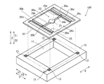
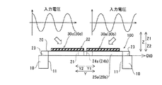
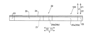
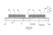
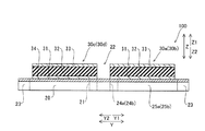
【解決手段】この振動ミラー素子100は、ベース部材10と、ミラー部21と、ミラー部21を両側から揺動可能に支持するとともに下部電極として機能する可動部22と、可動部22を支持するとともにベース部材10に取り付けられる取り付け部23とが一体的に形成されたチタンからなる基板20と、基板20の可動部22上に設けられるとともに、周期的な電圧が印加されることによりミラー部21を振動させる圧電膜32と、圧電膜32上に設けられた上部電極33とを備える。
【選択図】図1
Description
20 基板
21 ミラー部
22 可動部
23 取り付け部
24a、24b 回動軸部
25a、25b 変形部
32 圧電膜
31 中間層
100 振動ミラー素子
Claims (7)
- ベース部材と、
ミラー部と、前記ミラー部を両側から揺動可能に支持するとともに下部電極として機能する可動部と、前記可動部を支持するとともに前記ベース部材に取り付けられる取り付け部とが一体的に形成された金属からなる基板と、
前記基板の前記可動部上に設けられるとともに、周期的な電圧が印加されることにより前記ミラー部を振動させる圧電膜と、
前記圧電膜上に設けられた上部電極とを備えた、振動ミラー素子。 - 前記基板は、チタンまたはチタン合金により形成されている、請求項1に記載の振動ミラー素子。
- 前記取り付け部は、前記可動部および前記ミラー部を取り囲むように枠状に形成されている、請求項1または2に記載の振動ミラー素子。
- 前記可動部は、前記ミラー部に一方端が接続される一対の回動軸部と、前記一対の回動軸部の他方端にそれぞれ接続され、前記一対の回動軸部に対して略直交するように延びるとともに、2つの前記圧電膜が所定の間隔を隔てて一直線状にそれぞれ配置される一対の変形部とを含む、請求項3に記載の振動ミラー素子。
- 前記金属からなる基板の前記取り付け部は、前記ベース部材に半田接合により取り付けられている、請求項1〜4のいずれか1項に記載の振動ミラー素子。
- 前記基板は、正膨張係数を有する金属材料により形成され、
前記ベース部材は、負膨張係数材料により形成されている、請求項1〜5のいずれか1項に記載の振動ミラー素子。 - 前記圧電膜は鉛、チタンおよびジルコニウムを主成分とする酸化物により形成され、
前記金属からなる基板と前記圧電膜との間には、ペロブスカイト構造を有するとともにジルコニウムを含まない材料からなる中間層が形成されている、請求項1〜6のいずれか1項に記載の振動ミラー素子。
Priority Applications (6)
| Application Number | Priority Date | Filing Date | Title |
|---|---|---|---|
| JP2008184913A JP5391600B2 (ja) | 2008-07-16 | 2008-07-16 | 振動ミラー素子 |
| TW098123578A TWI463176B (zh) | 2008-07-16 | 2009-07-13 | 振動鏡元件 |
| US12/503,511 US8098415B2 (en) | 2008-07-16 | 2009-07-15 | Vibrating mirror element |
| CN2009101604597A CN101630063B (zh) | 2008-07-16 | 2009-07-15 | 振动镜元件 |
| KR1020090064379A KR20100008764A (ko) | 2008-07-16 | 2009-07-15 | 진동 미러 소자 |
| EP09251813A EP2146236A3 (en) | 2008-07-16 | 2009-07-16 | Vibrating mirror element |
Applications Claiming Priority (1)
| Application Number | Priority Date | Filing Date | Title |
|---|---|---|---|
| JP2008184913A JP5391600B2 (ja) | 2008-07-16 | 2008-07-16 | 振動ミラー素子 |
Publications (2)
| Publication Number | Publication Date |
|---|---|
| JP2010026069A true JP2010026069A (ja) | 2010-02-04 |
| JP5391600B2 JP5391600B2 (ja) | 2014-01-15 |
Family
ID=41226041
Family Applications (1)
| Application Number | Title | Priority Date | Filing Date |
|---|---|---|---|
| JP2008184913A Expired - Fee Related JP5391600B2 (ja) | 2008-07-16 | 2008-07-16 | 振動ミラー素子 |
Country Status (6)
| Country | Link |
|---|---|
| US (1) | US8098415B2 (ja) |
| EP (1) | EP2146236A3 (ja) |
| JP (1) | JP5391600B2 (ja) |
| KR (1) | KR20100008764A (ja) |
| CN (1) | CN101630063B (ja) |
| TW (1) | TWI463176B (ja) |
Cited By (7)
| Publication number | Priority date | Publication date | Assignee | Title |
|---|---|---|---|---|
| EP2827183A1 (en) * | 2013-07-17 | 2015-01-21 | Fujifilm Corporation | Mirror drive device and driving method thereof |
| US9331261B2 (en) | 2012-12-10 | 2016-05-03 | Panasonic Intellectual Property Management Co., Ltd. | Piezoelectric element |
| JP2016197265A (ja) * | 2012-05-07 | 2016-11-24 | パナソニックIpマネジメント株式会社 | 光学反射素子 |
| US9864189B2 (en) | 2013-07-17 | 2018-01-09 | Fujifilm Corporation | Mirror drive device and driving method thereof |
| US10018833B2 (en) | 2012-02-03 | 2018-07-10 | Funai Electric Co., Ltd. | MEMS device and electronic device having projector function |
| WO2023021777A1 (ja) * | 2021-08-19 | 2023-02-23 | パナソニックIpマネジメント株式会社 | 駆動素子 |
| WO2023136271A1 (ja) * | 2022-01-14 | 2023-07-20 | 北陽電機株式会社 | 梁、揺動素子および光走査装置 |
Families Citing this family (22)
| Publication number | Priority date | Publication date | Assignee | Title |
|---|---|---|---|---|
| US8522431B2 (en) | 2008-01-09 | 2013-09-03 | Féines Amatech Teoranta | Mounting and connecting an antenna wire in a transponder |
| JP4766353B2 (ja) * | 2009-09-28 | 2011-09-07 | 独立行政法人産業技術総合研究所 | 光ビーム走査装置 |
| CN102648577A (zh) * | 2009-11-19 | 2012-08-22 | 日本先锋公司 | 驱动装置 |
| JP5669443B2 (ja) * | 2010-05-31 | 2015-02-12 | キヤノン株式会社 | 振動体とその製造方法及び振動波アクチュエータ |
| WO2013027405A1 (ja) * | 2011-08-25 | 2013-02-28 | 株式会社ニコン | 空間光変調素子および露光装置 |
| JP5323155B2 (ja) * | 2011-09-08 | 2013-10-23 | 富士フイルム株式会社 | ミラー駆動装置及びその駆動方法並びに製造方法 |
| JP5857602B2 (ja) * | 2011-10-03 | 2016-02-10 | ミツミ電機株式会社 | 光走査装置 |
| EP2846370B1 (en) * | 2012-05-01 | 2016-07-06 | Konica Minolta, Inc. | Piezoelectric element |
| EP2874312B1 (en) * | 2012-07-11 | 2019-04-17 | Skyworks Filter Solutions Japan Co., Ltd. | Electronic component |
| JP2014126725A (ja) * | 2012-12-27 | 2014-07-07 | Funai Electric Co Ltd | 走査ミラー装置 |
| DE102013219583A1 (de) * | 2013-09-27 | 2015-04-02 | Carl Zeiss Smt Gmbh | Spiegel, insbesondere für eine mikrolithographische Projektionsbelichtungsanlage |
| DE102014217798A1 (de) | 2014-09-05 | 2016-03-10 | Fraunhofer-Gesellschaft zur Förderung der angewandten Forschung e.V. | Mikromechanische piezoelektrische Aktuatoren zur Realisierung hoher Kräfte und Auslenkungen |
| US10841548B2 (en) * | 2016-03-01 | 2020-11-17 | Funai Electric Co., Ltd. | Oscillating mirror element and projector |
| EP3264155B1 (en) * | 2016-06-29 | 2020-09-23 | Ricoh Company, Ltd. | Piezoelectric actuator, light deflector, and image projection device |
| WO2018088291A1 (ja) * | 2016-11-09 | 2018-05-17 | 第一精工株式会社 | 可動反射素子 |
| JP6924090B2 (ja) | 2017-07-21 | 2021-08-25 | 浜松ホトニクス株式会社 | アクチュエータ装置 |
| JP7386625B2 (ja) * | 2019-06-17 | 2023-11-27 | スタンレー電気株式会社 | 光偏向器の製造方法及び光偏向器 |
| CN112311977B (zh) * | 2019-07-26 | 2022-04-01 | 中芯集成电路(宁波)有限公司 | 成像模组及其形成方法、镜头组件 |
| US11175492B2 (en) | 2019-08-12 | 2021-11-16 | Microsoft Technology Licensing, Llc | Substrate for scanning mirror system |
| CN113130734A (zh) * | 2019-12-31 | 2021-07-16 | 中芯集成电路(宁波)有限公司 | 一种压电驱动结构和成像模组 |
| US11831255B2 (en) | 2020-04-25 | 2023-11-28 | Ultimems, Inc. | Scanner driven by piezoelectric actuators and method of making the same |
| CN112817145B (zh) * | 2021-01-05 | 2023-01-17 | 宁波大学 | 一种多层执行器阵列驱动的变形镜 |
Citations (11)
| Publication number | Priority date | Publication date | Assignee | Title |
|---|---|---|---|---|
| JPH11119145A (ja) * | 1997-10-16 | 1999-04-30 | Toshiba Corp | ガルバノミラーおよびこれを用いた光ディスク装置 |
| JP2005066727A (ja) * | 2003-08-21 | 2005-03-17 | Olympus Corp | 半導体装置 |
| JP2005128147A (ja) * | 2003-10-22 | 2005-05-19 | Stanley Electric Co Ltd | 光偏向器及び光学装置 |
| JP2005164859A (ja) * | 2003-12-01 | 2005-06-23 | Olympus Corp | 光偏向器アレイ |
| JP2005249645A (ja) * | 2004-03-05 | 2005-09-15 | Matsushita Electric Ind Co Ltd | 角速度センサおよびその製造方法 |
| JP2005308863A (ja) * | 2004-04-19 | 2005-11-04 | Ricoh Co Ltd | 偏向ミラー、光走査装置及び画像形成装置 |
| JP2005333108A (ja) * | 2004-04-02 | 2005-12-02 | Matsushita Electric Ind Co Ltd | 圧電素子、インクジェットヘッド、角速度センサ及びインクジェット式記録装置 |
| JP2005354026A (ja) * | 2004-05-10 | 2005-12-22 | Matsushita Electric Ind Co Ltd | 圧電素子及びインクジェットヘッド並びにそれらの製造方法、並びにインクジェット式記録装置 |
| JP2007268374A (ja) * | 2006-03-30 | 2007-10-18 | Brother Ind Ltd | 振動素子、振動素子の製造方法、光走査装置、画像形成装置及び画像表示装置 |
| JP2008020540A (ja) * | 2006-07-11 | 2008-01-31 | Ricoh Co Ltd | 光走査装置及び画像形成装置 |
| JP2008083603A (ja) * | 2006-09-28 | 2008-04-10 | Brother Ind Ltd | 光走査素子、光走査装置、光走査型表示装置及び網膜走査型表示装置 |
Family Cites Families (21)
| Publication number | Priority date | Publication date | Assignee | Title |
|---|---|---|---|---|
| JPH07181414A (ja) | 1993-12-22 | 1995-07-21 | Omron Corp | 光スキャナ |
| US5861979A (en) | 1994-01-18 | 1999-01-19 | Daewoo Electronics Co., Ltd. | Array of thin film actuated mirrors having an improved optical efficiency and an increased performance |
| KR950024553A (ko) | 1994-01-18 | 1995-08-21 | 배순훈 | 광로조절장치 및 제조방법 |
| JPH08306980A (ja) | 1995-03-08 | 1996-11-22 | Fuji Electric Co Ltd | 圧電素子ユニット及びその製造方法並びにその圧電素子ユニットを用いたインクジェット記録ヘッド |
| JPH10242795A (ja) | 1997-02-26 | 1998-09-11 | Matsushita Electric Ind Co Ltd | 圧電素子とその製造方法 |
| US5768009A (en) * | 1997-04-18 | 1998-06-16 | E-Beam | Light valve target comprising electrostatically-repelled micro-mirrors |
| WO1999000989A1 (en) * | 1997-06-30 | 1999-01-07 | Daewoo Electronics Co., Ltd. | Thin film actuated mirror including a seeding member and an electrodisplacive member made of materials having the same crystal structure and growth direction |
| CN2354150Y (zh) * | 1998-12-30 | 1999-12-15 | 中国科学院光电技术研究所 | 新型集成式多元压电变形反射镜 |
| CN1258854A (zh) * | 1998-12-30 | 2000-07-05 | 中国科学院光电技术研究所 | 集成式多元压电变形反射镜 |
| US6784771B1 (en) * | 2001-07-24 | 2004-08-31 | New Peregrine, Inc. | MEMS optical mirror array |
| US6844952B2 (en) * | 2001-09-18 | 2005-01-18 | Vitesse Semiconductor Corporation | Actuator-controlled mirror with Z-stop mechanism |
| DE10359102A1 (de) * | 2003-12-17 | 2005-07-21 | Carl Zeiss Smt Ag | Optische Komponente umfassend ein Material mit einer vorbestimmten Homogenität der thermischen Längsausdehnung |
| JP5221037B2 (ja) * | 2005-01-05 | 2013-06-26 | 日本電信電話株式会社 | ミラー装置 |
| JP4691704B2 (ja) * | 2005-04-13 | 2011-06-01 | 独立行政法人産業技術総合研究所 | 光走査装置 |
| JP2007149317A (ja) | 2005-10-26 | 2007-06-14 | Funai Electric Co Ltd | 可変形ミラー及びそれを備えた光ピックアップ装置 |
| JP2007199682A (ja) * | 2005-12-27 | 2007-08-09 | Konica Minolta Holdings Inc | 光偏向器および光ビーム走査装置 |
| JP4893067B2 (ja) | 2006-03-30 | 2012-03-07 | ブラザー工業株式会社 | 振動素子、振動素子の製造方法、光走査装置、画像形成装置及び画像表示装置 |
| JP2008040299A (ja) * | 2006-08-09 | 2008-02-21 | Funai Electric Co Ltd | 形状可変ミラー及び形状可変ミラーの製造方法 |
| JP4245015B2 (ja) * | 2006-08-11 | 2009-03-25 | セイコーエプソン株式会社 | 有機エレクトロルミネッセンス装置、有機エレクトロルミネッセンス装置の製造方法並びに電子機器 |
| US8390912B2 (en) * | 2007-01-10 | 2013-03-05 | Seiko Epson Corporation | Actuator, optical scanner and image forming device |
| US8427727B2 (en) * | 2008-01-22 | 2013-04-23 | Alcatel Lucent | Oscillating mirror for image projection |
-
2008
- 2008-07-16 JP JP2008184913A patent/JP5391600B2/ja not_active Expired - Fee Related
-
2009
- 2009-07-13 TW TW098123578A patent/TWI463176B/zh not_active IP Right Cessation
- 2009-07-15 CN CN2009101604597A patent/CN101630063B/zh not_active Expired - Fee Related
- 2009-07-15 KR KR1020090064379A patent/KR20100008764A/ko not_active Withdrawn
- 2009-07-15 US US12/503,511 patent/US8098415B2/en not_active Expired - Fee Related
- 2009-07-16 EP EP09251813A patent/EP2146236A3/en not_active Withdrawn
Patent Citations (11)
| Publication number | Priority date | Publication date | Assignee | Title |
|---|---|---|---|---|
| JPH11119145A (ja) * | 1997-10-16 | 1999-04-30 | Toshiba Corp | ガルバノミラーおよびこれを用いた光ディスク装置 |
| JP2005066727A (ja) * | 2003-08-21 | 2005-03-17 | Olympus Corp | 半導体装置 |
| JP2005128147A (ja) * | 2003-10-22 | 2005-05-19 | Stanley Electric Co Ltd | 光偏向器及び光学装置 |
| JP2005164859A (ja) * | 2003-12-01 | 2005-06-23 | Olympus Corp | 光偏向器アレイ |
| JP2005249645A (ja) * | 2004-03-05 | 2005-09-15 | Matsushita Electric Ind Co Ltd | 角速度センサおよびその製造方法 |
| JP2005333108A (ja) * | 2004-04-02 | 2005-12-02 | Matsushita Electric Ind Co Ltd | 圧電素子、インクジェットヘッド、角速度センサ及びインクジェット式記録装置 |
| JP2005308863A (ja) * | 2004-04-19 | 2005-11-04 | Ricoh Co Ltd | 偏向ミラー、光走査装置及び画像形成装置 |
| JP2005354026A (ja) * | 2004-05-10 | 2005-12-22 | Matsushita Electric Ind Co Ltd | 圧電素子及びインクジェットヘッド並びにそれらの製造方法、並びにインクジェット式記録装置 |
| JP2007268374A (ja) * | 2006-03-30 | 2007-10-18 | Brother Ind Ltd | 振動素子、振動素子の製造方法、光走査装置、画像形成装置及び画像表示装置 |
| JP2008020540A (ja) * | 2006-07-11 | 2008-01-31 | Ricoh Co Ltd | 光走査装置及び画像形成装置 |
| JP2008083603A (ja) * | 2006-09-28 | 2008-04-10 | Brother Ind Ltd | 光走査素子、光走査装置、光走査型表示装置及び網膜走査型表示装置 |
Cited By (9)
| Publication number | Priority date | Publication date | Assignee | Title |
|---|---|---|---|---|
| US10018833B2 (en) | 2012-02-03 | 2018-07-10 | Funai Electric Co., Ltd. | MEMS device and electronic device having projector function |
| JP2016197265A (ja) * | 2012-05-07 | 2016-11-24 | パナソニックIpマネジメント株式会社 | 光学反射素子 |
| US9331261B2 (en) | 2012-12-10 | 2016-05-03 | Panasonic Intellectual Property Management Co., Ltd. | Piezoelectric element |
| EP2827183A1 (en) * | 2013-07-17 | 2015-01-21 | Fujifilm Corporation | Mirror drive device and driving method thereof |
| US9678335B2 (en) | 2013-07-17 | 2017-06-13 | Fujifilm Corporation | Mirror drive device and driving method thereof |
| US9864189B2 (en) | 2013-07-17 | 2018-01-09 | Fujifilm Corporation | Mirror drive device and driving method thereof |
| WO2023021777A1 (ja) * | 2021-08-19 | 2023-02-23 | パナソニックIpマネジメント株式会社 | 駆動素子 |
| WO2023136271A1 (ja) * | 2022-01-14 | 2023-07-20 | 北陽電機株式会社 | 梁、揺動素子および光走査装置 |
| JP2023103695A (ja) * | 2022-01-14 | 2023-07-27 | 北陽電機株式会社 | 梁、揺動素子および光走査装置 |
Also Published As
| Publication number | Publication date |
|---|---|
| EP2146236A2 (en) | 2010-01-20 |
| TW201007207A (en) | 2010-02-16 |
| US20100014143A1 (en) | 2010-01-21 |
| CN101630063A (zh) | 2010-01-20 |
| TWI463176B (zh) | 2014-12-01 |
| CN101630063B (zh) | 2013-06-19 |
| JP5391600B2 (ja) | 2014-01-15 |
| EP2146236A3 (en) | 2012-05-16 |
| KR20100008764A (ko) | 2010-01-26 |
| US8098415B2 (en) | 2012-01-17 |
Similar Documents
| Publication | Publication Date | Title |
|---|---|---|
| JP5391600B2 (ja) | 振動ミラー素子 | |
| US8508826B2 (en) | Meandering oscillator, optical reflecting element using meandering oscillator, and image projection device using meandering oscillator | |
| CN102959454B (zh) | 光学反射元件 | |
| CN103827725B (zh) | 光学反射元件 | |
| JP2014215534A (ja) | 光走査装置 | |
| JP2010148265A (ja) | ミアンダ形振動子およびこれを用いた光学反射素子 | |
| JP4193817B2 (ja) | アクチュエータ | |
| JP2011069954A (ja) | 光スキャナ | |
| JP2009258210A (ja) | 光学反射素子 | |
| JP2009265560A (ja) | 光学反射素子 | |
| JP2009186721A (ja) | 光学反射素子 | |
| JP2009258339A (ja) | 光学反射素子 | |
| JP2009223115A (ja) | 光学反射素子 | |
| JP2009210955A (ja) | 光スキャナ | |
| JP2013160891A (ja) | 振動ミラー素子およびプロジェクタ機能を有する電子機器 | |
| JP2007326204A (ja) | アクチュエータ | |
| JP2009192781A (ja) | 光学反射素子 | |
| JP2009217093A (ja) | 光学反射素子 | |
| JP2010060688A (ja) | 光学反射素子 | |
| JP5045532B2 (ja) | 光学反射素子 | |
| JP2001272626A (ja) | 光スキャナ | |
| JP5045463B2 (ja) | 光学反射素子 | |
| JP2011137911A (ja) | 振動ミラー素子 | |
| JP6960889B2 (ja) | 光走査装置およびその駆動方法 | |
| JP4175272B2 (ja) | アクチュエータ |
Legal Events
| Date | Code | Title | Description |
|---|---|---|---|
| A621 | Written request for application examination |
Free format text: JAPANESE INTERMEDIATE CODE: A621 Effective date: 20110715 |
|
| A521 | Request for written amendment filed |
Free format text: JAPANESE INTERMEDIATE CODE: A523 Effective date: 20110831 |
|
| A521 | Request for written amendment filed |
Free format text: JAPANESE INTERMEDIATE CODE: A821 Effective date: 20110902 |
|
| A977 | Report on retrieval |
Free format text: JAPANESE INTERMEDIATE CODE: A971007 Effective date: 20120618 |
|
| A131 | Notification of reasons for refusal |
Free format text: JAPANESE INTERMEDIATE CODE: A131 Effective date: 20120703 |
|
| A521 | Request for written amendment filed |
Free format text: JAPANESE INTERMEDIATE CODE: A523 Effective date: 20120831 |
|
| A711 | Notification of change in applicant |
Free format text: JAPANESE INTERMEDIATE CODE: A711 Effective date: 20120907 |
|
| A521 | Request for written amendment filed |
Free format text: JAPANESE INTERMEDIATE CODE: A821 Effective date: 20120910 |
|
| A131 | Notification of reasons for refusal |
Free format text: JAPANESE INTERMEDIATE CODE: A131 Effective date: 20130702 |
|
| A521 | Request for written amendment filed |
Free format text: JAPANESE INTERMEDIATE CODE: A523 Effective date: 20130828 |
|
| TRDD | Decision of grant or rejection written | ||
| A01 | Written decision to grant a patent or to grant a registration (utility model) |
Free format text: JAPANESE INTERMEDIATE CODE: A01 Effective date: 20130917 |
|
| A61 | First payment of annual fees (during grant procedure) |
Free format text: JAPANESE INTERMEDIATE CODE: A61 Effective date: 20130930 |
|
| R150 | Certificate of patent or registration of utility model |
Free format text: JAPANESE INTERMEDIATE CODE: R150 |
|
| LAPS | Cancellation because of no payment of annual fees |