JP2008227495A - 高効率整流器 - Google Patents
高効率整流器 Download PDFInfo
- Publication number
- JP2008227495A JP2008227495A JP2008059321A JP2008059321A JP2008227495A JP 2008227495 A JP2008227495 A JP 2008227495A JP 2008059321 A JP2008059321 A JP 2008059321A JP 2008059321 A JP2008059321 A JP 2008059321A JP 2008227495 A JP2008227495 A JP 2008227495A
- Authority
- JP
- Japan
- Prior art keywords
- layer
- region
- polysilicon
- titanium
- thickness
- Prior art date
- Legal status (The legal status is an assumption and is not a legal conclusion. Google has not performed a legal analysis and makes no representation as to the accuracy of the status listed.)
- Pending
Links
- ZOXJGFHDIHLPTG-UHFFFAOYSA-N Boron Chemical compound [B] ZOXJGFHDIHLPTG-UHFFFAOYSA-N 0.000 claims abstract description 33
- 229910052796 boron Inorganic materials 0.000 claims abstract description 31
- 239000004065 semiconductor Substances 0.000 claims abstract description 30
- 239000000758 substrate Substances 0.000 claims abstract description 27
- 229910052710 silicon Inorganic materials 0.000 claims abstract description 21
- 239000010703 silicon Substances 0.000 claims abstract description 21
- 229910021341 titanium silicide Inorganic materials 0.000 claims abstract description 21
- 238000000151 deposition Methods 0.000 claims abstract description 15
- 238000004519 manufacturing process Methods 0.000 claims abstract description 13
- 229910021420 polycrystalline silicon Inorganic materials 0.000 claims description 30
- 229920005591 polysilicon Polymers 0.000 claims description 30
- 238000000034 method Methods 0.000 claims description 29
- XUIMIQQOPSSXEZ-UHFFFAOYSA-N Silicon Chemical compound [Si] XUIMIQQOPSSXEZ-UHFFFAOYSA-N 0.000 claims description 20
- 210000000746 body region Anatomy 0.000 claims description 17
- 229910021332 silicide Inorganic materials 0.000 claims description 16
- FVBUAEGBCNSCDD-UHFFFAOYSA-N silicide(4-) Chemical group [Si-4] FVBUAEGBCNSCDD-UHFFFAOYSA-N 0.000 claims description 15
- VYPSYNLAJGMNEJ-UHFFFAOYSA-N Silicium dioxide Chemical compound O=[Si]=O VYPSYNLAJGMNEJ-UHFFFAOYSA-N 0.000 claims description 14
- 229910052814 silicon oxide Inorganic materials 0.000 claims description 14
- RTAQQCXQSZGOHL-UHFFFAOYSA-N Titanium Chemical compound [Ti] RTAQQCXQSZGOHL-UHFFFAOYSA-N 0.000 claims description 13
- 239000010936 titanium Substances 0.000 claims description 13
- 229910052719 titanium Inorganic materials 0.000 claims description 13
- 239000002019 doping agent Substances 0.000 claims description 12
- 238000000206 photolithography Methods 0.000 claims description 10
- NRTOMJZYCJJWKI-UHFFFAOYSA-N Titanium nitride Chemical compound [Ti]#N NRTOMJZYCJJWKI-UHFFFAOYSA-N 0.000 claims description 9
- 229910052785 arsenic Inorganic materials 0.000 claims description 8
- RQNWIZPPADIBDY-UHFFFAOYSA-N arsenic atom Chemical compound [As] RQNWIZPPADIBDY-UHFFFAOYSA-N 0.000 claims description 8
- 150000003376 silicon Chemical class 0.000 claims description 5
- 238000005530 etching Methods 0.000 claims description 4
- 238000002513 implantation Methods 0.000 claims description 4
- 230000008569 process Effects 0.000 claims description 4
- OAICVXFJPJFONN-UHFFFAOYSA-N Phosphorus Chemical compound [P] OAICVXFJPJFONN-UHFFFAOYSA-N 0.000 claims description 2
- 230000001590 oxidative effect Effects 0.000 claims description 2
- 229910052698 phosphorus Inorganic materials 0.000 claims description 2
- 239000011574 phosphorus Substances 0.000 claims description 2
- 229920002120 photoresistant polymer Polymers 0.000 claims description 2
- 238000001020 plasma etching Methods 0.000 claims description 2
- 229920006395 saturated elastomer Polymers 0.000 abstract 1
- 230000004888 barrier function Effects 0.000 description 8
- 230000015556 catabolic process Effects 0.000 description 8
- 229910052751 metal Inorganic materials 0.000 description 7
- 239000002184 metal Substances 0.000 description 7
- 230000009467 reduction Effects 0.000 description 6
- 239000007943 implant Substances 0.000 description 5
- 230000006872 improvement Effects 0.000 description 5
- 230000015572 biosynthetic process Effects 0.000 description 3
- 238000010586 diagram Methods 0.000 description 3
- 230000005641 tunneling Effects 0.000 description 3
- 238000000231 atomic layer deposition Methods 0.000 description 2
- 238000006731 degradation reaction Methods 0.000 description 2
- 230000008021 deposition Effects 0.000 description 2
- 230000003071 parasitic effect Effects 0.000 description 2
- 238000004544 sputter deposition Methods 0.000 description 2
- 229910052782 aluminium Inorganic materials 0.000 description 1
- XAGFODPZIPBFFR-UHFFFAOYSA-N aluminium Chemical compound [Al] XAGFODPZIPBFFR-UHFFFAOYSA-N 0.000 description 1
- 239000012298 atmosphere Substances 0.000 description 1
- 150000001638 boron Chemical class 0.000 description 1
- 239000002131 composite material Substances 0.000 description 1
- 230000007547 defect Effects 0.000 description 1
- 239000006023 eutectic alloy Substances 0.000 description 1
- 230000002349 favourable effect Effects 0.000 description 1
- -1 for example Inorganic materials 0.000 description 1
- PCHJSUWPFVWCPO-UHFFFAOYSA-N gold Chemical compound [Au] PCHJSUWPFVWCPO-UHFFFAOYSA-N 0.000 description 1
- 229910052737 gold Inorganic materials 0.000 description 1
- 239000010931 gold Substances 0.000 description 1
- 230000003993 interaction Effects 0.000 description 1
- 238000001459 lithography Methods 0.000 description 1
- 238000001451 molecular beam epitaxy Methods 0.000 description 1
- 239000012299 nitrogen atmosphere Substances 0.000 description 1
- 230000000149 penetrating effect Effects 0.000 description 1
- 230000001681 protective effect Effects 0.000 description 1
- 238000005546 reactive sputtering Methods 0.000 description 1
- 238000011084 recovery Methods 0.000 description 1
- 229910052709 silver Inorganic materials 0.000 description 1
- 239000004332 silver Substances 0.000 description 1
- 229910000679 solder Inorganic materials 0.000 description 1
- 238000006467 substitution reaction Methods 0.000 description 1
Images


Classifications
-
- H—ELECTRICITY
- H01—ELECTRIC ELEMENTS
- H01L—SEMICONDUCTOR DEVICES NOT COVERED BY CLASS H10
- H01L29/00—Semiconductor devices adapted for rectifying, amplifying, oscillating or switching, or capacitors or resistors with at least one potential-jump barrier or surface barrier, e.g. PN junction depletion layer or carrier concentration layer; Details of semiconductor bodies or of electrodes thereof ; Multistep manufacturing processes therefor
- H01L29/02—Semiconductor bodies ; Multistep manufacturing processes therefor
- H01L29/36—Semiconductor bodies ; Multistep manufacturing processes therefor characterised by the concentration or distribution of impurities in the bulk material
- H01L29/365—Planar doping, e.g. atomic-plane doping, delta-doping
-
- H—ELECTRICITY
- H01—ELECTRIC ELEMENTS
- H01L—SEMICONDUCTOR DEVICES NOT COVERED BY CLASS H10
- H01L29/00—Semiconductor devices adapted for rectifying, amplifying, oscillating or switching, or capacitors or resistors with at least one potential-jump barrier or surface barrier, e.g. PN junction depletion layer or carrier concentration layer; Details of semiconductor bodies or of electrodes thereof ; Multistep manufacturing processes therefor
- H01L29/66—Types of semiconductor device ; Multistep manufacturing processes therefor
- H01L29/66007—Multistep manufacturing processes
- H01L29/66075—Multistep manufacturing processes of devices having semiconductor bodies comprising group 14 or group 13/15 materials
- H01L29/66083—Multistep manufacturing processes of devices having semiconductor bodies comprising group 14 or group 13/15 materials the devices being controllable only by variation of the electric current supplied or the electric potential applied, to one or more of the electrodes carrying the current to be rectified, amplified, oscillated or switched, e.g. two-terminal devices
- H01L29/6609—Diodes
- H01L29/66136—PN junction diodes
-
- H—ELECTRICITY
- H01—ELECTRIC ELEMENTS
- H01L—SEMICONDUCTOR DEVICES NOT COVERED BY CLASS H10
- H01L29/00—Semiconductor devices adapted for rectifying, amplifying, oscillating or switching, or capacitors or resistors with at least one potential-jump barrier or surface barrier, e.g. PN junction depletion layer or carrier concentration layer; Details of semiconductor bodies or of electrodes thereof ; Multistep manufacturing processes therefor
- H01L29/66—Types of semiconductor device ; Multistep manufacturing processes therefor
- H01L29/66007—Multistep manufacturing processes
- H01L29/66075—Multistep manufacturing processes of devices having semiconductor bodies comprising group 14 or group 13/15 materials
- H01L29/66083—Multistep manufacturing processes of devices having semiconductor bodies comprising group 14 or group 13/15 materials the devices being controllable only by variation of the electric current supplied or the electric potential applied, to one or more of the electrodes carrying the current to be rectified, amplified, oscillated or switched, e.g. two-terminal devices
- H01L29/6609—Diodes
- H01L29/66151—Tunnel diodes
-
- H—ELECTRICITY
- H01—ELECTRIC ELEMENTS
- H01L—SEMICONDUCTOR DEVICES NOT COVERED BY CLASS H10
- H01L29/00—Semiconductor devices adapted for rectifying, amplifying, oscillating or switching, or capacitors or resistors with at least one potential-jump barrier or surface barrier, e.g. PN junction depletion layer or carrier concentration layer; Details of semiconductor bodies or of electrodes thereof ; Multistep manufacturing processes therefor
- H01L29/66—Types of semiconductor device ; Multistep manufacturing processes therefor
- H01L29/66007—Multistep manufacturing processes
- H01L29/66075—Multistep manufacturing processes of devices having semiconductor bodies comprising group 14 or group 13/15 materials
- H01L29/66227—Multistep manufacturing processes of devices having semiconductor bodies comprising group 14 or group 13/15 materials the devices being controllable only by the electric current supplied or the electric potential applied, to an electrode which does not carry the current to be rectified, amplified or switched, e.g. three-terminal devices
- H01L29/66356—Gated diodes, e.g. field controlled diodes [FCD], static induction thyristors [SITh], field controlled thyristors [FCTh]
-
- H—ELECTRICITY
- H01—ELECTRIC ELEMENTS
- H01L—SEMICONDUCTOR DEVICES NOT COVERED BY CLASS H10
- H01L29/00—Semiconductor devices adapted for rectifying, amplifying, oscillating or switching, or capacitors or resistors with at least one potential-jump barrier or surface barrier, e.g. PN junction depletion layer or carrier concentration layer; Details of semiconductor bodies or of electrodes thereof ; Multistep manufacturing processes therefor
- H01L29/66—Types of semiconductor device ; Multistep manufacturing processes therefor
- H01L29/68—Types of semiconductor device ; Multistep manufacturing processes therefor controllable by only the electric current supplied, or only the electric potential applied, to an electrode which does not carry the current to be rectified, amplified or switched
- H01L29/70—Bipolar devices
- H01L29/72—Transistor-type devices, i.e. able to continuously respond to applied control signals
- H01L29/739—Transistor-type devices, i.e. able to continuously respond to applied control signals controlled by field-effect, e.g. bipolar static induction transistors [BSIT]
- H01L29/7391—Gated diode structures
-
- H—ELECTRICITY
- H01—ELECTRIC ELEMENTS
- H01L—SEMICONDUCTOR DEVICES NOT COVERED BY CLASS H10
- H01L29/00—Semiconductor devices adapted for rectifying, amplifying, oscillating or switching, or capacitors or resistors with at least one potential-jump barrier or surface barrier, e.g. PN junction depletion layer or carrier concentration layer; Details of semiconductor bodies or of electrodes thereof ; Multistep manufacturing processes therefor
- H01L29/66—Types of semiconductor device ; Multistep manufacturing processes therefor
- H01L29/86—Types of semiconductor device ; Multistep manufacturing processes therefor controllable only by variation of the electric current supplied, or only the electric potential applied, to one or more of the electrodes carrying the current to be rectified, amplified, oscillated or switched
- H01L29/861—Diodes
- H01L29/8618—Diodes with bulk potential barrier, e.g. Camel diodes, Planar Doped Barrier diodes, Graded bandgap diodes
-
- H—ELECTRICITY
- H01—ELECTRIC ELEMENTS
- H01L—SEMICONDUCTOR DEVICES NOT COVERED BY CLASS H10
- H01L29/00—Semiconductor devices adapted for rectifying, amplifying, oscillating or switching, or capacitors or resistors with at least one potential-jump barrier or surface barrier, e.g. PN junction depletion layer or carrier concentration layer; Details of semiconductor bodies or of electrodes thereof ; Multistep manufacturing processes therefor
- H01L29/66—Types of semiconductor device ; Multistep manufacturing processes therefor
- H01L29/86—Types of semiconductor device ; Multistep manufacturing processes therefor controllable only by variation of the electric current supplied, or only the electric potential applied, to one or more of the electrodes carrying the current to be rectified, amplified, oscillated or switched
- H01L29/861—Diodes
- H01L29/868—PIN diodes
-
- H—ELECTRICITY
- H01—ELECTRIC ELEMENTS
- H01L—SEMICONDUCTOR DEVICES NOT COVERED BY CLASS H10
- H01L29/00—Semiconductor devices adapted for rectifying, amplifying, oscillating or switching, or capacitors or resistors with at least one potential-jump barrier or surface barrier, e.g. PN junction depletion layer or carrier concentration layer; Details of semiconductor bodies or of electrodes thereof ; Multistep manufacturing processes therefor
- H01L29/66—Types of semiconductor device ; Multistep manufacturing processes therefor
- H01L29/86—Types of semiconductor device ; Multistep manufacturing processes therefor controllable only by variation of the electric current supplied, or only the electric potential applied, to one or more of the electrodes carrying the current to be rectified, amplified, oscillated or switched
- H01L29/861—Diodes
- H01L29/88—Tunnel-effect diodes
-
- H—ELECTRICITY
- H01—ELECTRIC ELEMENTS
- H01L—SEMICONDUCTOR DEVICES NOT COVERED BY CLASS H10
- H01L29/00—Semiconductor devices adapted for rectifying, amplifying, oscillating or switching, or capacitors or resistors with at least one potential-jump barrier or surface barrier, e.g. PN junction depletion layer or carrier concentration layer; Details of semiconductor bodies or of electrodes thereof ; Multistep manufacturing processes therefor
- H01L29/02—Semiconductor bodies ; Multistep manufacturing processes therefor
- H01L29/06—Semiconductor bodies ; Multistep manufacturing processes therefor characterised by their shape; characterised by the shapes, relative sizes, or dispositions of the semiconductor regions ; characterised by the concentration or distribution of impurities within semiconductor regions
- H01L29/0603—Semiconductor bodies ; Multistep manufacturing processes therefor characterised by their shape; characterised by the shapes, relative sizes, or dispositions of the semiconductor regions ; characterised by the concentration or distribution of impurities within semiconductor regions characterised by particular constructional design considerations, e.g. for preventing surface leakage, for controlling electric field concentration or for internal isolations regions
- H01L29/0607—Semiconductor bodies ; Multistep manufacturing processes therefor characterised by their shape; characterised by the shapes, relative sizes, or dispositions of the semiconductor regions ; characterised by the concentration or distribution of impurities within semiconductor regions characterised by particular constructional design considerations, e.g. for preventing surface leakage, for controlling electric field concentration or for internal isolations regions for preventing surface leakage or controlling electric field concentration
- H01L29/0611—Semiconductor bodies ; Multistep manufacturing processes therefor characterised by their shape; characterised by the shapes, relative sizes, or dispositions of the semiconductor regions ; characterised by the concentration or distribution of impurities within semiconductor regions characterised by particular constructional design considerations, e.g. for preventing surface leakage, for controlling electric field concentration or for internal isolations regions for preventing surface leakage or controlling electric field concentration for increasing or controlling the breakdown voltage of reverse biased devices
- H01L29/0615—Semiconductor bodies ; Multistep manufacturing processes therefor characterised by their shape; characterised by the shapes, relative sizes, or dispositions of the semiconductor regions ; characterised by the concentration or distribution of impurities within semiconductor regions characterised by particular constructional design considerations, e.g. for preventing surface leakage, for controlling electric field concentration or for internal isolations regions for preventing surface leakage or controlling electric field concentration for increasing or controlling the breakdown voltage of reverse biased devices by the doping profile or the shape or the arrangement of the PN junction, or with supplementary regions, e.g. junction termination extension [JTE]
- H01L29/0619—Semiconductor bodies ; Multistep manufacturing processes therefor characterised by their shape; characterised by the shapes, relative sizes, or dispositions of the semiconductor regions ; characterised by the concentration or distribution of impurities within semiconductor regions characterised by particular constructional design considerations, e.g. for preventing surface leakage, for controlling electric field concentration or for internal isolations regions for preventing surface leakage or controlling electric field concentration for increasing or controlling the breakdown voltage of reverse biased devices by the doping profile or the shape or the arrangement of the PN junction, or with supplementary regions, e.g. junction termination extension [JTE] with a supplementary region doped oppositely to or in rectifying contact with the semiconductor containing or contacting region, e.g. guard rings with PN or Schottky junction
Abstract
【解決手段】δP++層(12)、P−ボディ(14)、N−ドリフト領域(16)、N+基板(18)、アノード(20)、及びカソード(22)を含む高効率電力半導体整流デバイス(10)が開示される。デバイス(10)を製造する方法は、N+基板(18)上にN−ドリフト領域(16)を堆積させる段階と、N+ドリフト領域(16)内にホウ素を注入してP−ボディ領域(14)を作成する段階と、P−ボディ領域(14)上にチタンシリサイドの層(56)を形成する段階と、注入ホウ素の一部分をチタンシリサイドの層(56)とP−ボディ領域(14)の間のインタフェース領域で濃縮し、過飽和P−ドープシリコンのδP++層(12)を作成する段階とを含む。
【選択図】図1
Description
本発明のこれら及び他の特徴は、[発明を実施するための最良の形態]の節で以下に詳細に説明する。
本発明は、明確にするために寸法通りでなく大幅に強調された添付図面を参照して本明細書に説明する。
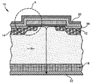
広義に特徴付ければ、デバイス10は、第1の導電型のドーパントで過飽和されたシリコンの層と、過飽和シリコンの層に実質的に隣接して位置する第1の導電型のボディ領域と、ボディ領域に実質的に隣接して位置する第2の導電型のドリフト領域と、ドリフト領域よりも下方に位置する第2の導電型の基板とを含む。
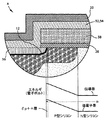
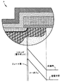
ゲート電圧がなければ、デバイス10は、ピンダイオードとしての機能を果たす。正のゲート電圧の印加は、ゲート誘電体の下部の2次元電子チャンネルとトンネリングδP+/N+接合の形成とをもたらす。
逆方向バイアスの印加は、負のゲートバイアスをもたらし、P−ボディ14の表面が反転しなくなり、デバイス10がP−i−Nダイオードとして機能するようになる。図4は、逆方向バイアスダイオードに関するダイオードの半導体表面に対する帯域図を示している。より高い逆方向バイパスは、P−ボディ14の表面がより蓄積状態になることをもたらし、次に、そのことが逆方向漏れ電流を低下させる。
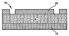
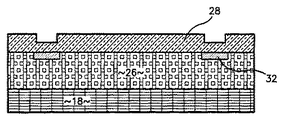
段階1:図5に示すように、N−ドリフト領域16であることになるN−層26が、シリコンN+基板18上にエピタキシャル堆積される。
段階2:図6に示すように、初期酸化シリコン層28が、N−層の上に成長する。一実施形態では、酸化シリコン層28は、約0.75マイクロメートルの厚みを有し、別の実施形態では、この厚みは、約0.5マイクロメートルから1.0マイクロメートルである。
段階6:図9に示すように、酸化シリコン28が第2のフォトリソグラフィ段階においてチップの中央でエッチングされて、活性区域34が開放される。
段階7:図10に示すように、ゲート酸化物36が活性区域34内部に成長する。一実施形態では、ゲート酸化物36は、約85Åの厚みを有する。
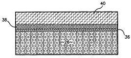
段階8:図11に示すように、ポリシリコンが堆積され、ポリシリコン層38が作成される。一実施形態では、ポリシリコン層38は、1500Åの厚みを有する。
段階10:図12に示すように、ポリシリコン層38が部分的に酸化されて、約800Åのポリシリコンが酸化されずに残され、高度N−ドープポリシリコンゲート40が作成される。
段階11:図13に示すように、ゲートは、第3のリソグラフィ段階においてエッチングされ、すなわち、更に形成される。
段階13:図15に示すように、ポリシリコン層38がエッチングされる。一実施形態では、このエッチングは、反応性イオンエッチング法を用いて達成される。
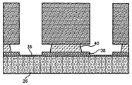
段階14:図16に示すように、ホウ素がN−ドリフト領域に注入され、P−ボディ14であることになるホウ素注入領域46が作成される。一実施形態では、ホウ素注入の線量は、約3e13cm−2であり、エネルギは、約80keVである。
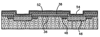
段階16:図18に示すように、上部酸化シリコン38及びポリシリコン域の外側のゲート酸化物36が、ゲートポリシリコン、P−ボディ14、及び段階17で付加されるチタン/窒化チタンがスパッタリングされた金属システムの間の良好な接触を保証するためにエッチングされる。
段階18:図20を参照すると、チタンシリサイドの層56が形成される。接触域内のある一定の量のシリコンが、650℃又はそれよりも高い温度でチタンシリサイド56に変換される。接触域内のホウ素は、チタンシリサイドとシリコンの間のインタフェース領域に移動又は「雪かき」され、約数個の原子層の厚みを有する過飽和PドープシリコンのδP++層12が作成される。
段階20:アノードは、第4のフォトリソグラフィ段階においてそのパターンを形成するためにエッチングされる。
段階22:カソード22又は裏面金属が、ウェーハのカソード側に堆積される。使用される金属システムは、例えば、半田又は共晶合金であるカソード接点の種類に依存することになる。
本発明を様々な特定的な実施形態に関連して開示したが、特許請求の範囲に説明した本発明の範囲を逸脱することなく、本明細書に均等物を用い、かつ置換を行うことができることは理解される。
本発明の好ましい実施形態をこのように説明したが、新規であると主張し、かつ特許証による保護が望ましい事項は、特許請求の範囲に含まれている。
12 δP++層
14 P−ボディ
16 N−ドリフト領域
18 N+基板
20 アノード
22 カソード
56 チタンシリサイドの層
Claims (36)
- 第1の導電型のドーパントにより過飽和された過飽和シリコンの層と、
実質的に前記過飽和シリコンの層の下方に該層に隣接して配置された前記第1の導電型のボディ領域と、
実質的に前記ボディ領域の下方に該領域に隣接して配置された第2の導電型のドリフト領域と、
実質的に前記ドリフト領域の下方に配置された前記第2の導電型の基板と、
を具備することを特徴とする半導体整流デバイス。 - 実質的に前記過飽和シリコンの層の上方に該層に隣接して配置され高次シリサイドを含むシリサイド領域、を更に具備する、請求項1に記載の半導体整流デバイス。
- δP++層と、
実質的に前記δP++層の下方に該層に隣接して配置されたP−ボディと、
実質的に前記P−ボディ領域の下方に該領域に隣接して配置されたN−ドリフト領域と、
実質的に前記N−ドリフト領域の下方に配置されたN+基板と、
を具備することを特徴とする半導体整流デバイス。 - 実質的に前記δP++層の上方に配置されたアノードと、
実質的に前記N+基板の下方に配置されたカソードと、を更に具備する、請求項3に記載の半導体整流デバイス。 - 前記δP++層は、P−ドープシリコンの過飽和領域を含みかつ約数個の原子層の厚みを有する、請求項3に記載の半導体整流デバイス。
- 前記N−ドリフト領域が、約0.4オーム−センチメートルの抵抗率及び約3マイクロメートルの厚みを有する、請求項3に記載の半導体整流デバイス。
- 前記N+基板が約5×10⁻³オーム−センチメートル以下の抵抗率を有する、請求項3に記載の半導体整流デバイス。
- 前記N+基板がヒ素によりドープされる、請求項7に記載の半導体整流デバイス。
- 前記N+基板が燐によりドープされる、請求項7に記載の半導体整流デバイス。
- 実質的に前記δP++層の上方に該層に隣接して配置された高次シリサイドの領域を更に具備する、請求項3に記載の半導体整流デバイス。
- 前記N−ドリフト領域、前記P−ボディ、前記δP++層、及び、前記チタンシリサイドの領域のうちの1つ以上の実質的に上方に隣接して配置され、ゲート誘電体として機能する酸化物の層を更に具備する、請求項10に記載の半導体整流デバイス。
- 前記酸化物が約85Åの厚みを有する、請求項11に記載の半導体整流デバイス。
- 実質的に前記酸化物の層の上方に該層に隣接して配置されたポリシリコンの層を更に具備する、請求項11に記載の半導体整流デバイス。
- 前記ポリシリコンの層が約40keVのエネルギでヒ素を注入される、請求項13に記載の半導体整流デバイス。
- 実質的に前記ポリシリコンの層の上方に該層に隣接して配置されたチタンの層を更に具備する、請求項13に記載の半導体整流デバイス。
- 前記チタンが約300Åの厚みを有する、請求項15に記載の半導体整流デバイス。
- 実質的に前記チタンの層の上方に該層に隣接して配置された窒化チタンの層を更に具備する、請求項15に記載の半導体整流デバイス。
- 前記窒化チタンの層が約500Åの厚みを有する、請求項16に記載の半導体整流デバイス。
- 半導体整流デバイスを製造する方法であって、
(a)第2の導電型のドリフト領域を該第2の導電型の基板上に堆積させる段階と、
(b)前記ドリフト領域内に第1の導電型のドーパントを注入して該第1の導電型のボディ領域を作成する段階と、
(c)前記ボディ領域上に高次シリサイドの層を形成する段階と、
(d)前記注入ドーパントの一部分を前記高次シリサイドの層と前記ボディ領域の間のインタフェース領域で濃縮し、前記第1の導電型の該ドーパントで過飽和されたシリコンの層を作成する段階と、
を含むことを特徴とする方法。 - 前記高次シリサイドの層がチタンシリサイドを含む、請求項19に記載の方法。
- 半導体整流デバイスを製造する方法であって、
(a)N+基板上にN−ドリフト領域を堆積させる段階と、
(b)前記N−ドリフト領域内にホウ素を注入してP−ボディ領域を作成する段階と、
(c)前記P−ボディ領域上にチタンシリサイドの層を形成する段階と、
(d)前記注入ホウ素の一部分を前記チタンシリサイドの層と前記P−ボディ領域の間のインタフェース領域で濃縮し、過飽和P−ドープシリコンのδP++層を作成する段階と、
を含むことを特徴とする方法。 - 前記δP++層が約数個の原子層の厚みを有する、請求項21に記載の方法。
- 半導体整流デバイスを製造する方法であって、
(a)シリコンN+基板上にN−層を堆積させる段階と、
(b)前記N−層の上に酸化シリコンの層を成長させる段階と、
(c)前記酸化シリコンの層の第1の部分を除去することにより、保護リングを形成する第1のフォトリソグラフィ段階を実行する段階と、
(d)前記保護リング内にホウ素を注入してホウ素注入領域を作成する段階と、
(e)前記ホウ素注入領域を拡散させる段階と、
(f)前記ホウ素注入領域の上に前記酸化シリコンの層の前記第1の部分を再成長させる段階と、
(g)前記酸化シリコンの層の第2の部分を除去して活性区域を開放する第2のフォトリソグラフィ段階を実行する段階と、
(h)前記活性区域内にゲート酸化物を成長させる段階と、
(i)前記ゲート酸化物上にポリシリコンの層を堆積させる段階と、
(j)前記ポリシリコンの層にヒ素を注入する段階と、
(k)前記ポリシリコンの層を部分酸化し、酸化ポリシリコンの層と非酸化ポリシリコンの層とを作成し、結果としてNドープポリシリコンゲートをもたらす段階と、
(l)前記ポリシリコンゲートを更に形成する第3のフォトリソグラフィ段階を実行する段階と、
(m)反応性イオンエッチング処理を用いて前記酸化ポリシリコンの層をエッチングする段階と、
(n)前記N−ドリフト領域内にホウ素を注入してP−ボディ領域を作成する段階と、
(o)フォトレジストを除去する段階と、
(p)前記酸化ポリシリコンの層と前記ゲート酸化物の上面とをエッチングする段階と、
(q)前記酸化ポリシリコンの層と前記ゲート酸化物の上にチタンの層を堆積させ、かつ該チタンの層の上に窒化チタンの層を堆積させる段階と、
(r)前記酸化ポリシリコンの層の一部分を少なくとも約650℃の温度に露出することによって前記P−ボディ領域と前記チタンの層の間にチタンシリサイドの層を形成し、結果としてホウ素をインタフェースまで移動させ、該チタンシリサイドの層と該P−ボディ領域の間に過飽和P−ドープシリコンのδP++層を作成する段階と、
を含むことを特徴とする方法。 - 段階(b)の前記酸化シリコンが約0.5マイクロメートルから1.0マイクロメートルの厚みに成長させられる、請求項23に記載の方法。
- 段階(h)の前記ゲート酸化物が約85Åの厚みに成長させられる、請求項23に記載の方法。
- 段階(i)の前記ポリシリコンが約1500Åの厚みに成長させられる、請求項23に記載の方法。
- 段階(j)において、前記ヒ素が約40keVのエネルギで注入される、請求項23に記載の方法。
- 前記非酸化ポリシリコンの層が約800Åの厚みを有する、請求項23に記載の方法。
- 段階(o)において、前記ホウ素が約80keVのエネルギで注入される、請求項23に記載の方法。
- 段階(q)において、前記ホウ素が約30keVのエネルギで注入される、請求項23に記載の方法。
- 段階(q)において、前記チタンの層が300Åの厚みを有し、前記窒化チタンの層が500Åの厚みを有する、請求項23に記載の方法。
- 段階(t)において、前記δP++層が約数個の原子層の厚みを有する、請求項23に記載の方法。
- アノードを堆積させる段階を更に含む、請求項23に記載の方法。
- 前記アノードをエッチングする第4のフォトリソグラフィ処理を実行する段階を更に含む、請求項23に記載の方法。
- 前記N+基板を薄くする段階を更に含む、請求項23に記載の方法。
- カソードを堆積させる段階を更に含む、請求項23に記載の方法。
Applications Claiming Priority (1)
| Application Number | Priority Date | Filing Date | Title |
|---|---|---|---|
| US11/684,261 US7847315B2 (en) | 2007-03-09 | 2007-03-09 | High efficiency rectifier |
Publications (2)
| Publication Number | Publication Date |
|---|---|
| JP2008227495A true JP2008227495A (ja) | 2008-09-25 |
| JP2008227495A5 JP2008227495A5 (ja) | 2011-04-21 |
Family
ID=39740792
Family Applications (1)
| Application Number | Title | Priority Date | Filing Date |
|---|---|---|---|
| JP2008059321A Pending JP2008227495A (ja) | 2007-03-09 | 2008-03-10 | 高効率整流器 |
Country Status (5)
| Country | Link |
|---|---|
| US (1) | US7847315B2 (ja) |
| EP (1) | EP2051291A3 (ja) |
| JP (1) | JP2008227495A (ja) |
| CN (1) | CN101271926B (ja) |
| TW (1) | TWI442564B (ja) |
Cited By (1)
| Publication number | Priority date | Publication date | Assignee | Title |
|---|---|---|---|---|
| JP2020061547A (ja) * | 2018-10-11 | 2020-04-16 | 朋程科技股▲ふん▼有限公司 | 車両用整流装置、整流器、発電装置及びパワートレイン |
Families Citing this family (11)
| Publication number | Priority date | Publication date | Assignee | Title |
|---|---|---|---|---|
| US8435873B2 (en) | 2006-06-08 | 2013-05-07 | Texas Instruments Incorporated | Unguarded Schottky barrier diodes with dielectric underetch at silicide interface |
| TWI381455B (zh) * | 2008-04-22 | 2013-01-01 | Pfc Device Co | 金氧半p-n接面二極體結構及其製作方法 |
| US8518811B2 (en) | 2011-04-08 | 2013-08-27 | Infineon Technologies Ag | Schottky diodes having metal gate electrodes and methods of formation thereof |
| JP5501539B1 (ja) | 2012-09-13 | 2014-05-21 | パナソニック株式会社 | 半導体装置 |
| WO2014168430A1 (ko) * | 2013-04-10 | 2014-10-16 | 주식회사 실리콘웍스 | 정류 회로의 제조 방법 |
| JP2015041644A (ja) * | 2013-08-20 | 2015-03-02 | 富士電機株式会社 | Mos型半導体装置の製造方法 |
| WO2015046791A1 (ko) * | 2013-09-26 | 2015-04-02 | 주식회사 실리콘웍스 | 반도체 정류 디바이스 및 그의 제조 방법 |
| CN104392899A (zh) * | 2014-10-08 | 2015-03-04 | 程德明 | 整流单晶硅片免喷砂扩散镀镍工艺 |
| TWI703736B (zh) * | 2018-10-11 | 2020-09-01 | 朋程科技股份有限公司 | 車用整流裝置、整流器、發電裝置以及動力系統 |
| CN109585572A (zh) * | 2018-12-29 | 2019-04-05 | 矽力杰半导体技术(杭州)有限公司 | 半导体器件及其制造方法 |
| JP7189848B2 (ja) * | 2019-08-07 | 2022-12-14 | 株式会社東芝 | 半導体装置およびその製造方法 |
Citations (6)
| Publication number | Priority date | Publication date | Assignee | Title |
|---|---|---|---|---|
| JPH0291974A (ja) * | 1988-09-29 | 1990-03-30 | Nippon Telegr & Teleph Corp <Ntt> | 半導体装置 |
| JPH04369272A (ja) * | 1991-06-18 | 1992-12-22 | Fuji Electric Co Ltd | 複合化ダイオード |
| JPH05275705A (ja) * | 1992-03-25 | 1993-10-22 | Shindengen Electric Mfg Co Ltd | 絶縁ゲ−ト型電界効果トランジスタとその製造方法 |
| JPH06310725A (ja) * | 1993-04-21 | 1994-11-04 | Mitsubishi Electric Corp | 半導体装置およびその製造方法 |
| JPH0997912A (ja) * | 1995-07-27 | 1997-04-08 | Origin Electric Co Ltd | 半導体ダイオード |
| JPH11154744A (ja) * | 1997-11-20 | 1999-06-08 | Origin Electric Co Ltd | Mos制御デバイス |
Family Cites Families (8)
| Publication number | Priority date | Publication date | Assignee | Title |
|---|---|---|---|---|
| GB1573309A (en) * | 1976-03-24 | 1980-08-20 | Mullard Ltd | Semiconductor devices and their manufacture |
| US4692348A (en) * | 1984-06-21 | 1987-09-08 | International Business Machines Corporation | Low temperature shallow doping technique |
| US5182222A (en) * | 1991-06-26 | 1993-01-26 | Texas Instruments Incorporated | Process for manufacturing a DMOS transistor |
| JP2773474B2 (ja) * | 1991-08-06 | 1998-07-09 | 日本電気株式会社 | 半導体装置 |
| US5818084A (en) | 1996-05-15 | 1998-10-06 | Siliconix Incorporated | Pseudo-Schottky diode |
| DE10217610B4 (de) * | 2002-04-19 | 2005-11-03 | Infineon Technologies Ag | Metall-Halbleiter-Kontakt, Halbleiterbauelement, integrierte Schaltungsanordnung und Verfahren |
| US6979861B2 (en) | 2002-05-30 | 2005-12-27 | Apd Semiconductor, Inc. | Power device having reduced reverse bias leakage current |
| US7417266B1 (en) * | 2004-06-10 | 2008-08-26 | Qspeed Semiconductor Inc. | MOSFET having a JFET embedded as a body diode |
-
2007
- 2007-03-09 US US11/684,261 patent/US7847315B2/en active Active
-
2008
- 2008-01-10 EP EP08000340A patent/EP2051291A3/en not_active Withdrawn
- 2008-03-07 TW TW097107982A patent/TWI442564B/zh active
- 2008-03-10 JP JP2008059321A patent/JP2008227495A/ja active Pending
- 2008-03-10 CN CN200810086033.7A patent/CN101271926B/zh active Active
Patent Citations (6)
| Publication number | Priority date | Publication date | Assignee | Title |
|---|---|---|---|---|
| JPH0291974A (ja) * | 1988-09-29 | 1990-03-30 | Nippon Telegr & Teleph Corp <Ntt> | 半導体装置 |
| JPH04369272A (ja) * | 1991-06-18 | 1992-12-22 | Fuji Electric Co Ltd | 複合化ダイオード |
| JPH05275705A (ja) * | 1992-03-25 | 1993-10-22 | Shindengen Electric Mfg Co Ltd | 絶縁ゲ−ト型電界効果トランジスタとその製造方法 |
| JPH06310725A (ja) * | 1993-04-21 | 1994-11-04 | Mitsubishi Electric Corp | 半導体装置およびその製造方法 |
| JPH0997912A (ja) * | 1995-07-27 | 1997-04-08 | Origin Electric Co Ltd | 半導体ダイオード |
| JPH11154744A (ja) * | 1997-11-20 | 1999-06-08 | Origin Electric Co Ltd | Mos制御デバイス |
Cited By (2)
| Publication number | Priority date | Publication date | Assignee | Title |
|---|---|---|---|---|
| JP2020061547A (ja) * | 2018-10-11 | 2020-04-16 | 朋程科技股▲ふん▼有限公司 | 車両用整流装置、整流器、発電装置及びパワートレイン |
| US11508808B2 (en) | 2018-10-11 | 2022-11-22 | Actron Technology Corporation | Rectifier device, rectifier, generator device, and powertrain for vehicle |
Also Published As
| Publication number | Publication date |
|---|---|
| CN101271926B (zh) | 2013-04-17 |
| TW200901462A (en) | 2009-01-01 |
| EP2051291A3 (en) | 2011-06-29 |
| US20080217721A1 (en) | 2008-09-11 |
| TWI442564B (zh) | 2014-06-21 |
| CN101271926A (zh) | 2008-09-24 |
| US7847315B2 (en) | 2010-12-07 |
| EP2051291A2 (en) | 2009-04-22 |
Similar Documents
| Publication | Publication Date | Title |
|---|---|---|
| US7847315B2 (en) | High efficiency rectifier | |
| CN106876485B (zh) | 一种集成肖特基二极管的SiC双沟槽型MOSFET器件及其制备方法 | |
| US11342420B2 (en) | Heterojunction devices and methods for fabricating the same | |
| US7282753B2 (en) | Vertical conducting power semiconducting devices made by deep reactive ion etching | |
| JP5525940B2 (ja) | 半導体装置および半導体装置の製造方法 | |
| US9209242B2 (en) | Semiconductor device with an edge termination structure having a closed vertical trench | |
| TWI520327B (zh) | 用於製備陽極短路的場欄絕緣閘雙極電晶體之方法 | |
| CN102751320B (zh) | 半导体器件 | |
| US10304930B2 (en) | Semiconductor device implanted with arsenic and nitrogen | |
| TW201242022A (en) | Transistors with high concentration of boron doped germanium | |
| US10410911B2 (en) | Buried insulator regions and methods of formation thereof | |
| US20080246055A1 (en) | Semiconductor component including a monocrystalline semiconductor body and method | |
| JP2008130699A (ja) | ワイドバンドギャップ半導体装置およびその製造方法 | |
| CN108010964B (zh) | 一种igbt器件及制造方法 | |
| EP1090428A1 (en) | Punch-through diode and method of manufacturing the same | |
| JP2011171421A (ja) | 半導体装置およびその製造方法 | |
| JP5028749B2 (ja) | 半導体装置の製造方法 | |
| CN110931548A (zh) | 一种半导体器件结构及其制造方法 | |
| WO2015111177A1 (ja) | 半導体装置,パワーモジュール,電力変換装置,および鉄道車両 | |
| JP2008103392A (ja) | 半導体装置および半導体装置の製造方法 | |
| JPH10335630A (ja) | 半導体装置及びその製造方法 | |
| TW201737351A (zh) | 溝槽式二極體和用於製造此種二極體之方法 | |
| US20220115532A1 (en) | Power semiconductor device and manufacturing method therefor | |
| CN117995841A (zh) | 一种lvff碳化硅场效应管及制备工艺 | |
| JPH1197717A (ja) | ショットキバリアダイオードの製造方法 |
Legal Events
| Date | Code | Title | Description |
|---|---|---|---|
| A521 | Written amendment |
Free format text: JAPANESE INTERMEDIATE CODE: A523 Effective date: 20110304 |
|
| A621 | Written request for application examination |
Free format text: JAPANESE INTERMEDIATE CODE: A621 Effective date: 20110304 |
|
| A977 | Report on retrieval |
Free format text: JAPANESE INTERMEDIATE CODE: A971007 Effective date: 20130116 |
|
| A131 | Notification of reasons for refusal |
Free format text: JAPANESE INTERMEDIATE CODE: A131 Effective date: 20130121 |
|
| A601 | Written request for extension of time |
Free format text: JAPANESE INTERMEDIATE CODE: A601 Effective date: 20130412 |
|
| A602 | Written permission of extension of time |
Free format text: JAPANESE INTERMEDIATE CODE: A602 Effective date: 20130417 |
|
| A02 | Decision of refusal |
Free format text: JAPANESE INTERMEDIATE CODE: A02 Effective date: 20131021 |