JP2007508698A - 有機ケイ酸塩ガラスについての一酸化二窒素剥脱方法 - Google Patents
有機ケイ酸塩ガラスについての一酸化二窒素剥脱方法 Download PDFInfo
- Publication number
- JP2007508698A JP2007508698A JP2006534260A JP2006534260A JP2007508698A JP 2007508698 A JP2007508698 A JP 2007508698A JP 2006534260 A JP2006534260 A JP 2006534260A JP 2006534260 A JP2006534260 A JP 2006534260A JP 2007508698 A JP2007508698 A JP 2007508698A
- Authority
- JP
- Japan
- Prior art keywords
- layer
- photoresist
- osg
- stripping
- organic
- Prior art date
- Legal status (The legal status is an assumption and is not a legal conclusion. Google has not performed a legal analysis and makes no representation as to the accuracy of the status listed.)
- Pending
Links
- 238000000034 method Methods 0.000 title claims abstract description 94
- GQPLMRYTRLFLPF-UHFFFAOYSA-N Nitrous Oxide Chemical compound [O-][N+]#N GQPLMRYTRLFLPF-UHFFFAOYSA-N 0.000 title claims abstract description 20
- 238000004299 exfoliation Methods 0.000 title claims abstract description 19
- 239000011521 glass Substances 0.000 title claims abstract description 12
- 229960001730 nitrous oxide Drugs 0.000 title claims abstract description 10
- 235000013842 nitrous oxide Nutrition 0.000 title claims abstract description 8
- 229920002120 photoresistant polymer Polymers 0.000 claims abstract description 104
- 239000000463 material Substances 0.000 claims abstract description 42
- 230000008569 process Effects 0.000 claims abstract description 17
- 230000009977 dual effect Effects 0.000 claims abstract description 13
- 238000005530 etching Methods 0.000 claims description 43
- VYPSYNLAJGMNEJ-UHFFFAOYSA-N Silicium dioxide Chemical group O=[Si]=O VYPSYNLAJGMNEJ-UHFFFAOYSA-N 0.000 claims description 8
- 229910004298 SiO 2 Inorganic materials 0.000 claims description 6
- XUIMIQQOPSSXEZ-UHFFFAOYSA-N Silicon Chemical compound [Si] XUIMIQQOPSSXEZ-UHFFFAOYSA-N 0.000 claims description 6
- 229910052710 silicon Inorganic materials 0.000 claims description 6
- 239000010703 silicon Substances 0.000 claims description 6
- 229910052581 Si3N4 Inorganic materials 0.000 claims description 5
- HBMJWWWQQXIZIP-UHFFFAOYSA-N silicon carbide Chemical compound [Si+]#[C-] HBMJWWWQQXIZIP-UHFFFAOYSA-N 0.000 claims description 5
- HQVNEWCFYHHQES-UHFFFAOYSA-N silicon nitride Chemical group N12[Si]34N5[Si]62N3[Si]51N64 HQVNEWCFYHHQES-UHFFFAOYSA-N 0.000 claims description 5
- 239000000377 silicon dioxide Substances 0.000 claims description 4
- 235000012239 silicon dioxide Nutrition 0.000 claims description 4
- NRTOMJZYCJJWKI-UHFFFAOYSA-N Titanium nitride Chemical compound [Ti]#N NRTOMJZYCJJWKI-UHFFFAOYSA-N 0.000 claims description 3
- MZLGASXMSKOWSE-UHFFFAOYSA-N tantalum nitride Chemical compound [Ta]#N MZLGASXMSKOWSE-UHFFFAOYSA-N 0.000 claims description 3
- 239000000203 mixture Substances 0.000 abstract description 15
- 239000011368 organic material Substances 0.000 abstract description 8
- 230000002411 adverse Effects 0.000 abstract 1
- 239000007789 gas Substances 0.000 description 28
- 239000006117 anti-reflective coating Substances 0.000 description 16
- 230000004888 barrier function Effects 0.000 description 10
- 238000012545 processing Methods 0.000 description 10
- IJGRMHOSHXDMSA-UHFFFAOYSA-N Atomic nitrogen Chemical compound N#N IJGRMHOSHXDMSA-UHFFFAOYSA-N 0.000 description 8
- 239000004065 semiconductor Substances 0.000 description 7
- 235000012431 wafers Nutrition 0.000 description 7
- QGZKDVFQNNGYKY-UHFFFAOYSA-N Ammonia Chemical compound N QGZKDVFQNNGYKY-UHFFFAOYSA-N 0.000 description 6
- QVGXLLKOCUKJST-UHFFFAOYSA-N atomic oxygen Chemical group [O] QVGXLLKOCUKJST-UHFFFAOYSA-N 0.000 description 6
- 230000008901 benefit Effects 0.000 description 6
- 229910052760 oxygen Inorganic materials 0.000 description 6
- 239000001301 oxygen Substances 0.000 description 6
- 239000000758 substrate Substances 0.000 description 6
- 229910052757 nitrogen Inorganic materials 0.000 description 5
- 235000014653 Carica parviflora Nutrition 0.000 description 4
- 241000243321 Cnidaria Species 0.000 description 4
- 238000002474 experimental method Methods 0.000 description 4
- UFHFLCQGNIYNRP-UHFFFAOYSA-N Hydrogen Chemical compound [H][H] UFHFLCQGNIYNRP-UHFFFAOYSA-N 0.000 description 3
- 229910021529 ammonia Inorganic materials 0.000 description 3
- 230000008878 coupling Effects 0.000 description 3
- 238000010168 coupling process Methods 0.000 description 3
- 238000005859 coupling reaction Methods 0.000 description 3
- 239000003989 dielectric material Substances 0.000 description 3
- 239000001257 hydrogen Substances 0.000 description 3
- 229910052739 hydrogen Inorganic materials 0.000 description 3
- 238000009616 inductively coupled plasma Methods 0.000 description 3
- 239000011261 inert gas Substances 0.000 description 3
- 238000004519 manufacturing process Methods 0.000 description 3
- XKRFYHLGVUSROY-UHFFFAOYSA-N Argon Chemical compound [Ar] XKRFYHLGVUSROY-UHFFFAOYSA-N 0.000 description 2
- CURLTUGMZLYLDI-UHFFFAOYSA-N Carbon dioxide Chemical compound O=C=O CURLTUGMZLYLDI-UHFFFAOYSA-N 0.000 description 2
- RYGMFSIKBFXOCR-UHFFFAOYSA-N Copper Chemical compound [Cu] RYGMFSIKBFXOCR-UHFFFAOYSA-N 0.000 description 2
- 238000005033 Fourier transform infrared spectroscopy Methods 0.000 description 2
- 229910018540 Si C Inorganic materials 0.000 description 2
- 239000006227 byproduct Substances 0.000 description 2
- 229910052802 copper Inorganic materials 0.000 description 2
- 239000010949 copper Substances 0.000 description 2
- 239000010432 diamond Substances 0.000 description 2
- 238000011066 ex-situ storage Methods 0.000 description 2
- 239000001272 nitrous oxide Substances 0.000 description 2
- 239000002245 particle Substances 0.000 description 2
- 238000000206 photolithography Methods 0.000 description 2
- 229920000642 polymer Polymers 0.000 description 2
- 238000011160 research Methods 0.000 description 2
- 229910010271 silicon carbide Inorganic materials 0.000 description 2
- BSYNRYMUTXBXSQ-UHFFFAOYSA-N Aspirin Chemical compound CC(=O)OC1=CC=CC=C1C(O)=O BSYNRYMUTXBXSQ-UHFFFAOYSA-N 0.000 description 1
- 229910052786 argon Inorganic materials 0.000 description 1
- 230000015572 biosynthetic process Effects 0.000 description 1
- 229910002092 carbon dioxide Inorganic materials 0.000 description 1
- 239000001569 carbon dioxide Substances 0.000 description 1
- 230000008859 change Effects 0.000 description 1
- 238000005229 chemical vapour deposition Methods 0.000 description 1
- 238000004140 cleaning Methods 0.000 description 1
- 230000007423 decrease Effects 0.000 description 1
- 238000009792 diffusion process Methods 0.000 description 1
- 239000003085 diluting agent Substances 0.000 description 1
- 230000008020 evaporation Effects 0.000 description 1
- 238000001704 evaporation Methods 0.000 description 1
- 239000001307 helium Substances 0.000 description 1
- 229910052734 helium Inorganic materials 0.000 description 1
- SWQJXJOGLNCZEY-UHFFFAOYSA-N helium atom Chemical compound [He] SWQJXJOGLNCZEY-UHFFFAOYSA-N 0.000 description 1
- 238000011065 in-situ storage Methods 0.000 description 1
- 229910052743 krypton Inorganic materials 0.000 description 1
- DNNSSWSSYDEUBZ-UHFFFAOYSA-N krypton atom Chemical compound [Kr] DNNSSWSSYDEUBZ-UHFFFAOYSA-N 0.000 description 1
- 229910052754 neon Inorganic materials 0.000 description 1
- GKAOGPIIYCISHV-UHFFFAOYSA-N neon atom Chemical compound [Ne] GKAOGPIIYCISHV-UHFFFAOYSA-N 0.000 description 1
- 229910052756 noble gas Inorganic materials 0.000 description 1
- 150000002835 noble gases Chemical class 0.000 description 1
- 239000007800 oxidant agent Substances 0.000 description 1
- 230000003647 oxidation Effects 0.000 description 1
- 238000007254 oxidation reaction Methods 0.000 description 1
- 230000001590 oxidative effect Effects 0.000 description 1
- 229910021420 polycrystalline silicon Inorganic materials 0.000 description 1
- 229920005591 polysilicon Polymers 0.000 description 1
- 239000011148 porous material Substances 0.000 description 1
- 239000002210 silicon-based material Substances 0.000 description 1
- 239000002904 solvent Substances 0.000 description 1
- 229910052724 xenon Inorganic materials 0.000 description 1
- FHNFHKCVQCLJFQ-UHFFFAOYSA-N xenon atom Chemical compound [Xe] FHNFHKCVQCLJFQ-UHFFFAOYSA-N 0.000 description 1
Images


Classifications
-
- H—ELECTRICITY
- H01—ELECTRIC ELEMENTS
- H01L—SEMICONDUCTOR DEVICES NOT COVERED BY CLASS H10
- H01L21/00—Processes or apparatus adapted for the manufacture or treatment of semiconductor or solid state devices or of parts thereof
- H01L21/70—Manufacture or treatment of devices consisting of a plurality of solid state components formed in or on a common substrate or of parts thereof; Manufacture of integrated circuit devices or of parts thereof
- H01L21/71—Manufacture of specific parts of devices defined in group H01L21/70
- H01L21/768—Applying interconnections to be used for carrying current between separate components within a device comprising conductors and dielectrics
- H01L21/76801—Applying interconnections to be used for carrying current between separate components within a device comprising conductors and dielectrics characterised by the formation and the after-treatment of the dielectrics, e.g. smoothing
- H01L21/76802—Applying interconnections to be used for carrying current between separate components within a device comprising conductors and dielectrics characterised by the formation and the after-treatment of the dielectrics, e.g. smoothing by forming openings in dielectrics
- H01L21/76807—Applying interconnections to be used for carrying current between separate components within a device comprising conductors and dielectrics characterised by the formation and the after-treatment of the dielectrics, e.g. smoothing by forming openings in dielectrics for dual damascene structures
- H01L21/76808—Applying interconnections to be used for carrying current between separate components within a device comprising conductors and dielectrics characterised by the formation and the after-treatment of the dielectrics, e.g. smoothing by forming openings in dielectrics for dual damascene structures involving intermediate temporary filling with material
-
- G—PHYSICS
- G03—PHOTOGRAPHY; CINEMATOGRAPHY; ANALOGOUS TECHNIQUES USING WAVES OTHER THAN OPTICAL WAVES; ELECTROGRAPHY; HOLOGRAPHY
- G03F—PHOTOMECHANICAL PRODUCTION OF TEXTURED OR PATTERNED SURFACES, e.g. FOR PRINTING, FOR PROCESSING OF SEMICONDUCTOR DEVICES; MATERIALS THEREFOR; ORIGINALS THEREFOR; APPARATUS SPECIALLY ADAPTED THEREFOR
- G03F7/00—Photomechanical, e.g. photolithographic, production of textured or patterned surfaces, e.g. printing surfaces; Materials therefor, e.g. comprising photoresists; Apparatus specially adapted therefor
- G03F7/26—Processing photosensitive materials; Apparatus therefor
- G03F7/42—Stripping or agents therefor
-
- H—ELECTRICITY
- H01—ELECTRIC ELEMENTS
- H01L—SEMICONDUCTOR DEVICES NOT COVERED BY CLASS H10
- H01L21/00—Processes or apparatus adapted for the manufacture or treatment of semiconductor or solid state devices or of parts thereof
- H01L21/02—Manufacture or treatment of semiconductor devices or of parts thereof
- H01L21/04—Manufacture or treatment of semiconductor devices or of parts thereof the devices having potential barriers, e.g. a PN junction, depletion layer or carrier concentration layer
- H01L21/18—Manufacture or treatment of semiconductor devices or of parts thereof the devices having potential barriers, e.g. a PN junction, depletion layer or carrier concentration layer the devices having semiconductor bodies comprising elements of Group IV of the Periodic Table or AIIIBV compounds with or without impurities, e.g. doping materials
- H01L21/30—Treatment of semiconductor bodies using processes or apparatus not provided for in groups H01L21/20 - H01L21/26
- H01L21/31—Treatment of semiconductor bodies using processes or apparatus not provided for in groups H01L21/20 - H01L21/26 to form insulating layers thereon, e.g. for masking or by using photolithographic techniques; After treatment of these layers; Selection of materials for these layers
- H01L21/3105—After-treatment
- H01L21/311—Etching the insulating layers by chemical or physical means
- H01L21/31127—Etching organic layers
- H01L21/31133—Etching organic layers by chemical means
- H01L21/31138—Etching organic layers by chemical means by dry-etching
-
- H—ELECTRICITY
- H01—ELECTRIC ELEMENTS
- H01L—SEMICONDUCTOR DEVICES NOT COVERED BY CLASS H10
- H01L21/00—Processes or apparatus adapted for the manufacture or treatment of semiconductor or solid state devices or of parts thereof
- H01L21/70—Manufacture or treatment of devices consisting of a plurality of solid state components formed in or on a common substrate or of parts thereof; Manufacture of integrated circuit devices or of parts thereof
- H01L21/71—Manufacture of specific parts of devices defined in group H01L21/70
- H01L21/768—Applying interconnections to be used for carrying current between separate components within a device comprising conductors and dielectrics
- H01L21/76801—Applying interconnections to be used for carrying current between separate components within a device comprising conductors and dielectrics characterised by the formation and the after-treatment of the dielectrics, e.g. smoothing
- H01L21/76802—Applying interconnections to be used for carrying current between separate components within a device comprising conductors and dielectrics characterised by the formation and the after-treatment of the dielectrics, e.g. smoothing by forming openings in dielectrics
- H01L21/76807—Applying interconnections to be used for carrying current between separate components within a device comprising conductors and dielectrics characterised by the formation and the after-treatment of the dielectrics, e.g. smoothing by forming openings in dielectrics for dual damascene structures
- H01L21/76811—Applying interconnections to be used for carrying current between separate components within a device comprising conductors and dielectrics characterised by the formation and the after-treatment of the dielectrics, e.g. smoothing by forming openings in dielectrics for dual damascene structures involving multiple stacked pre-patterned masks
Landscapes
- Engineering & Computer Science (AREA)
- General Physics & Mathematics (AREA)
- Physics & Mathematics (AREA)
- Microelectronics & Electronic Packaging (AREA)
- Manufacturing & Machinery (AREA)
- Computer Hardware Design (AREA)
- Condensed Matter Physics & Semiconductors (AREA)
- Power Engineering (AREA)
- Chemical & Material Sciences (AREA)
- Chemical Kinetics & Catalysis (AREA)
- General Chemical & Material Sciences (AREA)
- Internal Circuitry In Semiconductor Integrated Circuit Devices (AREA)
- Drying Of Semiconductors (AREA)
Abstract
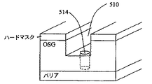
【解決手段】有機フォトレジスト材料と有機ケイ酸塩ガラス(OSG)材料を有する集積回路(IC)構造体において有機フォトレジストを剥脱する、デュアルダマシンプロセス中に行われる多数の工程の1つであって、一酸化二窒素(N2O)ガス混合物を反応器内に供給すること、反応器内でプラズマを発生させること、及びフォトレジストを剥脱することを含んでなる方法を提供する。この剥脱方法は、フォトレジストとOSG材料との間に高い選択性を提供し、さらに、フォトレジストや他のそのような有機材料の剥脱を、OSG材料のエッチングに用いられるのと同じ反応器内で行うことを可能とする。
【選択図】図1
Description

Claims (26)
- フォトレジスト材料及び有機ケイ酸塩ガラス(OSG)材料を有する集積回路(IC)構造体を剥脱する方法であって:
一酸化二窒素(N2O)ガスを反応器内へ供給すること;
前記反応器でプラズマを発生させること;
前記フォトレジストを剥脱すること;及び、
前記フォトレジスト及び前記OSG間に高い選択性を発生させること
を含んでなる方法。 - 前記フォトレジストが有機フォトレジストである、請求項1に記載の方法。
- 前記フォトレジストを前記剥脱することが、デュアルダマシンプロセス中に行われる多数の工程のうちの1つである、請求項2に記載の方法。
- 前記フォトレジストの前記剥脱が、前記OSG材料をエッチングするために用いられる同じ反応器内で行われる、請求項3に記載の方法。
- 請求項1に記載の方法であって、さらに:
前記IC構造体中にエッチングされたビアを提供すること;
前記ビアを占める有機プラグを生成すること;及び、
前記N2Oガスで前記有機プラグを剥脱すること
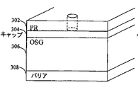
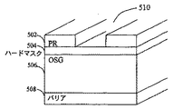
を含んでなる方法。 - 第一フォトレジスト層、第二中間層、および第三有機ケイ酸塩ガラス(OSG)層を含む集積回路(IC)構造体を剥脱する方法であって:
一酸化二窒素(N2O)を反応器内に供給すること;
前記反応器内にプラズマを発生させること;
前記プラズマで前記フォトレジストを剥脱すること;
前記第一フォトレジスト層及び前記第二ハードマスク層間に高い選択性を発生させること;及び、
前記第一フォトレジスト層及び前記第三OSG層間に高い選択性を発生させること
を含んでなる方法。 - 前記フォトレジストが有機フォトレジストである、請求項6に記載の方法。
- 前記フォトレジストの前記剥脱が、前記OSG層をエッチングするために用いられる同じ反応器内で行われる、請求項6に記載の方法。
- 前記フォトレジストを前記剥脱することが、デュアルダマシンプロセス中に行われる複数の工程のうちの1つである、請求項6に記載の方法。
- 前記第二中間層がキャップ層である、請求項6に記載の方法。
- 前記キャップ層が、二酸化ケイ素(SiO2)及びオキシ窒化ケイ素(SiON)からなる群から選ばれる、請求項10に記載の方法。
- 前記第二中間層がハードマスク層である、請求項6に記載の方法。
- 前記ハードマスク層が、窒化ケイ素(Si3N4)、窒化タンタル(TaN)、窒化チタン(TiN)、及び炭化ケイ素(SiC)からなる群から選ばれる、請求項12に記載の方法。
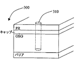
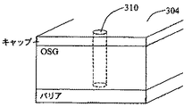
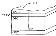
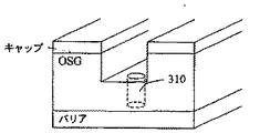
- 第一フォトレジスト層、第二キャップ層、及び第三有機ケイ酸塩ガラス(OSG)層を含むIC構造体でビアファーストエッチングを行う方法であって:
一番目に、前記第二キャップ層と前記第三OSG層の中に、ビアをエッチングすること;そして、
二番目に、前記第一フォトレジスト層を、一酸化二窒素(N2O)ガスで剥脱すること
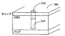
を含んでなる方法。 - 請求項14に記載の方法であって、三番目に、前記第三OSG層の一部を占める前記ビアで有機プラグを発生させることを、さらに含んでなる方法。
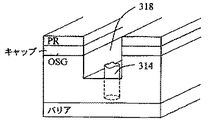
- 請求項15に記載の方法であって、四番目に、前記第二キャップ層及び前記第三OSG層中にトレンチをエッチングすることを、さらに含んでなる方法。
- 請求項15に記載の方法であって、五番目に、前記他の第一フォトレジスト層及び前記有機プラグを、前記N2Oガスで剥脱することを、さらに含んでなる方法。
- 前記フォトレジストが有機フォトレジストである、請求項17に記載の方法。
- 前記フォトレジストを前記剥脱することが、デュアルダマシンプロセス中に行われる多数の工程のうちの1つである、請求項18に記載の方法。
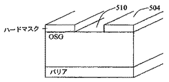
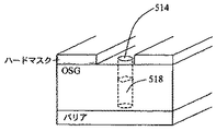
- 第一フォトレジスト層、第二ハードマスク層、および第三有機ケイ酸塩ガラス(OSG)層を含むIC構造体でトレンチファーストエッチングを行う方法であって:
一番目に、前記第二ハードマスク層の中にトレンチをエッチングすること;そして、
二番目に、前記第一フォトレジスト層を、一酸化二窒素(N2O)ガスで剥脱すること
を含んでなる方法。 - 請求項20に記載の方法であって、三番目に、ビアエッチングを行うために別の第一フォトレジスト層を塗布することを、さらに含んでなる方法。
- 請求項21に記載の方法であって、四番目に、前記第二ハードマスク層及び前記第三OSG層中にビアをエッチングすることを、さらに含んでなる方法。
- 請求項22に記載の方法であって、五番目に、前記他の第一フォトレジスト層を、前記N2Oガスで剥脱することを、さらに含んでなる方法。
- 請求項23に記載の方法であって、六番目に、前記第三OSG層の一部を占める前記ビア内に有機プラグを生成させることを、さらに含んでなる方法。
- 請求項24に記載の方法であって、七番目に、前記第三OSG層中に前記トレンチをエッチングすることを、さらに含んでなる方法。
- 請求項25に記載の方法であって、八番目に、前記有機プラグを剥脱するために前記N2Oガスを用いることを、さらに含んでなる方法。
Applications Claiming Priority (2)
| Application Number | Priority Date | Filing Date | Title |
|---|---|---|---|
| US10/680,895 US7202177B2 (en) | 2003-10-08 | 2003-10-08 | Nitrous oxide stripping process for organosilicate glass |
| PCT/US2004/032793 WO2005038892A1 (en) | 2003-10-08 | 2004-10-05 | A nitrous oxide stripping process for organosilicate glass |
Publications (2)
| Publication Number | Publication Date |
|---|---|
| JP2007508698A true JP2007508698A (ja) | 2007-04-05 |
| JP2007508698A5 JP2007508698A5 (ja) | 2007-10-18 |
Family
ID=34422202
Family Applications (1)
| Application Number | Title | Priority Date | Filing Date |
|---|---|---|---|
| JP2006534260A Pending JP2007508698A (ja) | 2003-10-08 | 2004-10-05 | 有機ケイ酸塩ガラスについての一酸化二窒素剥脱方法 |
Country Status (7)
| Country | Link |
|---|---|
| US (1) | US7202177B2 (ja) |
| EP (1) | EP1671363A4 (ja) |
| JP (1) | JP2007508698A (ja) |
| KR (1) | KR101197070B1 (ja) |
| CN (1) | CN100426469C (ja) |
| TW (1) | TW200523689A (ja) |
| WO (1) | WO2005038892A1 (ja) |
Cited By (1)
| Publication number | Priority date | Publication date | Assignee | Title |
|---|---|---|---|---|
| KR20190070859A (ko) * | 2017-12-13 | 2019-06-21 | 도쿄엘렉트론가부시키가이샤 | 반도체 장치의 제조 방법 |
Families Citing this family (9)
| Publication number | Priority date | Publication date | Assignee | Title |
|---|---|---|---|---|
| US20050136681A1 (en) * | 2003-12-23 | 2005-06-23 | Tokyo Electron Limited | Method and apparatus for removing photoresist from a substrate |
| KR100666881B1 (ko) * | 2005-06-10 | 2007-01-10 | 삼성전자주식회사 | 포토레지스트 제거 방법 및 이를 이용한 반도체 소자의제조 방법. |
| CN101310175A (zh) * | 2005-11-17 | 2008-11-19 | Nxp股份有限公司 | 湿度传感器 |
| US7932181B2 (en) * | 2006-06-20 | 2011-04-26 | Lam Research Corporation | Edge gas injection for critical dimension uniformity improvement |
| US8283255B2 (en) * | 2007-05-24 | 2012-10-09 | Lam Research Corporation | In-situ photoresist strip during plasma etching of active hard mask |
| US20100130017A1 (en) * | 2008-11-21 | 2010-05-27 | Axcelis Technologies, Inc. | Front end of line plasma mediated ashing processes and apparatus |
| US20110226280A1 (en) * | 2008-11-21 | 2011-09-22 | Axcelis Technologies, Inc. | Plasma mediated ashing processes |
| CN101996934B (zh) * | 2009-08-20 | 2012-07-18 | 中芯国际集成电路制造(上海)有限公司 | 半导体器件的制作方法 |
| CN115799028A (zh) * | 2021-09-10 | 2023-03-14 | 长鑫存储技术有限公司 | 半导体结构的制备方法及半导体结构 |
Citations (6)
| Publication number | Priority date | Publication date | Assignee | Title |
|---|---|---|---|---|
| JP2000183040A (ja) * | 1998-12-15 | 2000-06-30 | Canon Inc | 有機層間絶縁膜エッチング後のレジストアッシング方法 |
| WO2002003426A2 (en) * | 2000-06-30 | 2002-01-10 | Lam Research Corporation | Process for the post etch stripping of photoresist with hydrogen |
| JP2003045969A (ja) * | 2001-07-12 | 2003-02-14 | Samsung Electronics Co Ltd | デュアルダマシン工程を利用した配線形成方法 |
| JP2003092349A (ja) * | 2001-09-18 | 2003-03-28 | Mitsubishi Electric Corp | 半導体装置およびその製造方法 |
| US6617257B2 (en) * | 2001-03-30 | 2003-09-09 | Lam Research Corporation | Method of plasma etching organic antireflective coating |
| JP2003303880A (ja) * | 2002-04-10 | 2003-10-24 | Nec Corp | 積層層間絶縁膜構造を利用した配線構造およびその製造方法 |
Family Cites Families (18)
| Publication number | Priority date | Publication date | Assignee | Title |
|---|---|---|---|---|
| US111041A (en) * | 1871-01-17 | Improvement in hay-tedders | ||
| US5126231A (en) * | 1990-02-26 | 1992-06-30 | Applied Materials, Inc. | Process for multi-layer photoresist etching with minimal feature undercut and unchanging photoresist load during etch |
| US5910453A (en) * | 1996-01-16 | 1999-06-08 | Advanced Micro Devices, Inc. | Deep UV anti-reflection coating etch |
| US5970376A (en) * | 1997-12-29 | 1999-10-19 | Taiwan Semiconductor Manufacturing Company, Ltd. | Post via etch plasma treatment method for forming with attenuated lateral etching a residue free via through a silsesquioxane spin-on-glass (SOG) dielectric layer |
| JP4221847B2 (ja) * | 1999-10-25 | 2009-02-12 | パナソニック電工株式会社 | プラズマ処理装置及びプラズマ点灯方法 |
| US6323121B1 (en) * | 2000-05-12 | 2001-11-27 | Taiwan Semiconductor Manufacturing Company | Fully dry post-via-etch cleaning method for a damascene process |
| TW495822B (en) * | 2000-06-29 | 2002-07-21 | D M S Co Ltd | Apparatus for irradiating ultraviolet light |
| US6413877B1 (en) | 2000-12-22 | 2002-07-02 | Lam Research Corporation | Method of preventing damage to organo-silicate-glass materials during resist stripping |
| US6514860B1 (en) * | 2001-01-31 | 2003-02-04 | Advanced Micro Devices, Inc. | Integration of organic fill for dual damascene process |
| US6777344B2 (en) | 2001-02-12 | 2004-08-17 | Lam Research Corporation | Post-etch photoresist strip with O2 and NH3 for organosilicate glass low-K dielectric etch applications |
| US6566283B1 (en) * | 2001-02-15 | 2003-05-20 | Advanced Micro Devices, Inc. | Silane treatment of low dielectric constant materials in semiconductor device manufacturing |
| US20020139771A1 (en) * | 2001-02-22 | 2002-10-03 | Ping Jiang | Gas switching during an etch process to modulate the characteristics of the etch |
| US6498112B1 (en) | 2001-07-13 | 2002-12-24 | Advanced Micro Devices, Inc. | Graded oxide caps on low dielectric constant (low K) chemical vapor deposition (CVD) films |
| US6696222B2 (en) * | 2001-07-24 | 2004-02-24 | Silicon Integrated Systems Corp. | Dual damascene process using metal hard mask |
| US7253112B2 (en) * | 2002-06-04 | 2007-08-07 | Taiwan Semiconductor Manufacturing Co., Ltd. | Dual damascene process |
| JP2004079901A (ja) * | 2002-08-21 | 2004-03-11 | Nec Electronics Corp | 半導体装置及びその製造方法 |
| US6720256B1 (en) * | 2002-12-04 | 2004-04-13 | Taiwan Semiconductor Manufacturing Company | Method of dual damascene patterning |
| US6916697B2 (en) * | 2003-10-08 | 2005-07-12 | Lam Research Corporation | Etch back process using nitrous oxide |
-
2003
- 2003-10-08 US US10/680,895 patent/US7202177B2/en not_active Expired - Lifetime
-
2004
- 2004-10-04 TW TW093130026A patent/TW200523689A/zh unknown
- 2004-10-05 EP EP04794216A patent/EP1671363A4/en not_active Withdrawn
- 2004-10-05 JP JP2006534260A patent/JP2007508698A/ja active Pending
- 2004-10-05 KR KR1020067008588A patent/KR101197070B1/ko active IP Right Grant
- 2004-10-05 CN CNB2004800291641A patent/CN100426469C/zh not_active Expired - Fee Related
- 2004-10-05 WO PCT/US2004/032793 patent/WO2005038892A1/en active Application Filing
Patent Citations (6)
| Publication number | Priority date | Publication date | Assignee | Title |
|---|---|---|---|---|
| JP2000183040A (ja) * | 1998-12-15 | 2000-06-30 | Canon Inc | 有機層間絶縁膜エッチング後のレジストアッシング方法 |
| WO2002003426A2 (en) * | 2000-06-30 | 2002-01-10 | Lam Research Corporation | Process for the post etch stripping of photoresist with hydrogen |
| US6617257B2 (en) * | 2001-03-30 | 2003-09-09 | Lam Research Corporation | Method of plasma etching organic antireflective coating |
| JP2003045969A (ja) * | 2001-07-12 | 2003-02-14 | Samsung Electronics Co Ltd | デュアルダマシン工程を利用した配線形成方法 |
| JP2003092349A (ja) * | 2001-09-18 | 2003-03-28 | Mitsubishi Electric Corp | 半導体装置およびその製造方法 |
| JP2003303880A (ja) * | 2002-04-10 | 2003-10-24 | Nec Corp | 積層層間絶縁膜構造を利用した配線構造およびその製造方法 |
Cited By (6)
| Publication number | Priority date | Publication date | Assignee | Title |
|---|---|---|---|---|
| KR20190070859A (ko) * | 2017-12-13 | 2019-06-21 | 도쿄엘렉트론가부시키가이샤 | 반도체 장치의 제조 방법 |
| JP2019106490A (ja) * | 2017-12-13 | 2019-06-27 | 東京エレクトロン株式会社 | 半導体装置の製造方法 |
| CN110034063A (zh) * | 2017-12-13 | 2019-07-19 | 东京毅力科创株式会社 | 半导体装置的制造方法 |
| US11495490B2 (en) | 2017-12-13 | 2022-11-08 | Tokyo Electron Limited | Semiconductor device manufacturing method |
| CN110034063B (zh) * | 2017-12-13 | 2023-10-20 | 东京毅力科创株式会社 | 半导体装置的制造方法 |
| KR102642184B1 (ko) * | 2017-12-13 | 2024-03-04 | 도쿄엘렉트론가부시키가이샤 | 반도체 장치의 제조 방법 |
Also Published As
| Publication number | Publication date |
|---|---|
| KR20060107758A (ko) | 2006-10-16 |
| US20050079710A1 (en) | 2005-04-14 |
| EP1671363A1 (en) | 2006-06-21 |
| TW200523689A (en) | 2005-07-16 |
| CN1864249A (zh) | 2006-11-15 |
| EP1671363A4 (en) | 2010-01-13 |
| KR101197070B1 (ko) | 2012-11-06 |
| US7202177B2 (en) | 2007-04-10 |
| CN100426469C (zh) | 2008-10-15 |
| WO2005038892A1 (en) | 2005-04-28 |
Similar Documents
| Publication | Publication Date | Title |
|---|---|---|
| KR100849707B1 (ko) | 탄소-도우핑된 저유전체들의 선택적 식각 | |
| KR100883291B1 (ko) | 유기 반사 방지막 플라즈마 식각 방법 | |
| US6805139B1 (en) | Systems and methods for photoresist strip and residue treatment in integrated circuit manufacturing | |
| JP6049871B2 (ja) | エッチング及びアッシング中での低誘電率材料の側壁保護 | |
| KR100778260B1 (ko) | 수소로 포토레지스트를 포스트 에칭 박리하기 위한 프로세스 | |
| US6583065B1 (en) | Sidewall polymer forming gas additives for etching processes | |
| US6991739B2 (en) | Method of photoresist removal in the presence of a dielectric layer having a low k-value | |
| US6686293B2 (en) | Method of etching a trench in a silicon-containing dielectric material | |
| US20050022839A1 (en) | Systems and methods for photoresist strip and residue treatment in integrated circuit manufacturing | |
| TWI514516B (zh) | 保護外露式低k表面的方法 | |
| US6849193B2 (en) | Highly selective process for etching oxide over nitride using hexafluorobutadiene | |
| US20070193602A1 (en) | Systems and Methods for Photoresist Strip and Residue Treatment in Integrated Circuit Manufacturing | |
| JP2007537602A (ja) | フルオロカーボン化学エッチングにおけるh2添加物を使用しての炭素ドープ酸化ケイ素エッチング | |
| US7129171B2 (en) | Selective oxygen-free etching process for barrier materials | |
| JP4451934B2 (ja) | 導電層をエッチングする方法及び集積回路 | |
| KR20060123144A (ko) | 포토레지스트 스트립 동안의 배리어 재료의 손실 최소화 | |
| US6647994B1 (en) | Method of resist stripping over low-k dielectric material | |
| KR101197070B1 (ko) | 유기실리케이트 유리용 아산화질소 스트립 프로세스 | |
| KR101276043B1 (ko) | 아산화질소를 사용하는 에치백 프로세스 | |
| US6969685B1 (en) | Etching a dielectric layer in an integrated circuit structure having a metal hard mask layer |
Legal Events
| Date | Code | Title | Description |
|---|---|---|---|
| A521 | Request for written amendment filed |
Free format text: JAPANESE INTERMEDIATE CODE: A523 Effective date: 20070829 |
|
| A621 | Written request for application examination |
Free format text: JAPANESE INTERMEDIATE CODE: A621 Effective date: 20070829 |
|
| A977 | Report on retrieval |
Free format text: JAPANESE INTERMEDIATE CODE: A971007 Effective date: 20100817 |
|
| A131 | Notification of reasons for refusal |
Free format text: JAPANESE INTERMEDIATE CODE: A131 Effective date: 20100819 |
|
| A601 | Written request for extension of time |
Free format text: JAPANESE INTERMEDIATE CODE: A601 Effective date: 20101119 |
|
| A602 | Written permission of extension of time |
Free format text: JAPANESE INTERMEDIATE CODE: A602 Effective date: 20101129 |
|
| A601 | Written request for extension of time |
Free format text: JAPANESE INTERMEDIATE CODE: A601 Effective date: 20101220 |
|
| A602 | Written permission of extension of time |
Free format text: JAPANESE INTERMEDIATE CODE: A602 Effective date: 20101228 |
|
| A601 | Written request for extension of time |
Free format text: JAPANESE INTERMEDIATE CODE: A601 Effective date: 20110119 |
|
| A602 | Written permission of extension of time |
Free format text: JAPANESE INTERMEDIATE CODE: A602 Effective date: 20110126 |
|
| A521 | Request for written amendment filed |
Free format text: JAPANESE INTERMEDIATE CODE: A523 Effective date: 20110221 |
|
| A02 | Decision of refusal |
Free format text: JAPANESE INTERMEDIATE CODE: A02 Effective date: 20110414 |