JP2007227577A - 光起電力装置およびその製造方法 - Google Patents
光起電力装置およびその製造方法 Download PDFInfo
- Publication number
- JP2007227577A JP2007227577A JP2006046083A JP2006046083A JP2007227577A JP 2007227577 A JP2007227577 A JP 2007227577A JP 2006046083 A JP2006046083 A JP 2006046083A JP 2006046083 A JP2006046083 A JP 2006046083A JP 2007227577 A JP2007227577 A JP 2007227577A
- Authority
- JP
- Japan
- Prior art keywords
- electrode
- groove portion
- groove
- photoelectric conversion
- conversion unit
- Prior art date
- Legal status (The legal status is an assumption and is not a legal conclusion. Google has not performed a legal analysis and makes no representation as to the accuracy of the status listed.)
- Granted
Links
- 238000004519 manufacturing process Methods 0.000 title claims description 25
- 238000006243 chemical reaction Methods 0.000 claims abstract description 88
- 239000000758 substrate Substances 0.000 claims abstract description 72
- 230000008018 melting Effects 0.000 claims description 5
- 238000002844 melting Methods 0.000 claims description 5
- 238000000034 method Methods 0.000 claims description 4
- 239000011529 conductive interlayer Substances 0.000 abstract 2
- 239000011229 interlayer Substances 0.000 abstract 2
- 230000000452 restraining effect Effects 0.000 abstract 1
- 229910021417 amorphous silicon Inorganic materials 0.000 description 12
- 230000000052 comparative effect Effects 0.000 description 12
- 229910021424 microcrystalline silicon Inorganic materials 0.000 description 10
- XUIMIQQOPSSXEZ-UHFFFAOYSA-N Silicon Chemical compound [Si] XUIMIQQOPSSXEZ-UHFFFAOYSA-N 0.000 description 9
- 239000004065 semiconductor Substances 0.000 description 9
- 229910052710 silicon Inorganic materials 0.000 description 9
- 239000010703 silicon Substances 0.000 description 9
- BQCADISMDOOEFD-UHFFFAOYSA-N Silver Chemical compound [Ag] BQCADISMDOOEFD-UHFFFAOYSA-N 0.000 description 7
- 229910052709 silver Inorganic materials 0.000 description 7
- 239000004332 silver Substances 0.000 description 7
- 238000007650 screen-printing Methods 0.000 description 5
- 230000010355 oscillation Effects 0.000 description 4
- XLOMVQKBTHCTTD-UHFFFAOYSA-N Zinc monoxide Chemical compound [Zn]=O XLOMVQKBTHCTTD-UHFFFAOYSA-N 0.000 description 3
- 230000000694 effects Effects 0.000 description 3
- 239000003822 epoxy resin Substances 0.000 description 3
- 238000012986 modification Methods 0.000 description 3
- 230000004048 modification Effects 0.000 description 3
- TWNQGVIAIRXVLR-UHFFFAOYSA-N oxo(oxoalumanyloxy)alumane Chemical compound O=[Al]O[Al]=O TWNQGVIAIRXVLR-UHFFFAOYSA-N 0.000 description 3
- 239000002245 particle Substances 0.000 description 3
- 229920000647 polyepoxide Polymers 0.000 description 3
- 238000011109 contamination Methods 0.000 description 2
- 238000002474 experimental method Methods 0.000 description 2
- 238000005259 measurement Methods 0.000 description 2
- 239000007769 metal material Substances 0.000 description 2
- 238000005268 plasma chemical vapour deposition Methods 0.000 description 2
- HBMJWWWQQXIZIP-UHFFFAOYSA-N silicon carbide Chemical compound [Si+]#[C-] HBMJWWWQQXIZIP-UHFFFAOYSA-N 0.000 description 2
- 238000009751 slip forming Methods 0.000 description 2
- 238000004544 sputter deposition Methods 0.000 description 2
- XOLBLPGZBRYERU-UHFFFAOYSA-N tin dioxide Chemical compound O=[Sn]=O XOLBLPGZBRYERU-UHFFFAOYSA-N 0.000 description 2
- 229910001887 tin oxide Inorganic materials 0.000 description 2
- 229910018072 Al 2 O 3 Inorganic materials 0.000 description 1
- 229910006404 SnO 2 Inorganic materials 0.000 description 1
- 238000005229 chemical vapour deposition Methods 0.000 description 1
- 238000012790 confirmation Methods 0.000 description 1
- 230000006866 deterioration Effects 0.000 description 1
- 239000011521 glass Substances 0.000 description 1
- 238000009413 insulation Methods 0.000 description 1
- 239000000203 mixture Substances 0.000 description 1
- 229910010271 silicon carbide Inorganic materials 0.000 description 1
- 238000002230 thermal chemical vapour deposition Methods 0.000 description 1
- 239000011787 zinc oxide Substances 0.000 description 1
Images


Classifications
-
- H—ELECTRICITY
- H01—ELECTRIC ELEMENTS
- H01L—SEMICONDUCTOR DEVICES NOT COVERED BY CLASS H10
- H01L31/00—Semiconductor devices sensitive to infrared radiation, light, electromagnetic radiation of shorter wavelength or corpuscular radiation and specially adapted either for the conversion of the energy of such radiation into electrical energy or for the control of electrical energy by such radiation; Processes or apparatus specially adapted for the manufacture or treatment thereof or of parts thereof; Details thereof
- H01L31/18—Processes or apparatus specially adapted for the manufacture or treatment of these devices or of parts thereof
- H01L31/20—Processes or apparatus specially adapted for the manufacture or treatment of these devices or of parts thereof such devices or parts thereof comprising amorphous semiconductor materials
- H01L31/202—Processes or apparatus specially adapted for the manufacture or treatment of these devices or of parts thereof such devices or parts thereof comprising amorphous semiconductor materials including only elements of Group IV of the Periodic System
-
- H—ELECTRICITY
- H01—ELECTRIC ELEMENTS
- H01L—SEMICONDUCTOR DEVICES NOT COVERED BY CLASS H10
- H01L31/00—Semiconductor devices sensitive to infrared radiation, light, electromagnetic radiation of shorter wavelength or corpuscular radiation and specially adapted either for the conversion of the energy of such radiation into electrical energy or for the control of electrical energy by such radiation; Processes or apparatus specially adapted for the manufacture or treatment thereof or of parts thereof; Details thereof
- H01L31/04—Semiconductor devices sensitive to infrared radiation, light, electromagnetic radiation of shorter wavelength or corpuscular radiation and specially adapted either for the conversion of the energy of such radiation into electrical energy or for the control of electrical energy by such radiation; Processes or apparatus specially adapted for the manufacture or treatment thereof or of parts thereof; Details thereof adapted as photovoltaic [PV] conversion devices
- H01L31/042—PV modules or arrays of single PV cells
- H01L31/0445—PV modules or arrays of single PV cells including thin film solar cells, e.g. single thin film a-Si, CIS or CdTe solar cells
- H01L31/046—PV modules composed of a plurality of thin film solar cells deposited on the same substrate
- H01L31/0463—PV modules composed of a plurality of thin film solar cells deposited on the same substrate characterised by special patterning methods to connect the PV cells in a module, e.g. laser cutting of the conductive or active layers
-
- H—ELECTRICITY
- H01—ELECTRIC ELEMENTS
- H01L—SEMICONDUCTOR DEVICES NOT COVERED BY CLASS H10
- H01L31/00—Semiconductor devices sensitive to infrared radiation, light, electromagnetic radiation of shorter wavelength or corpuscular radiation and specially adapted either for the conversion of the energy of such radiation into electrical energy or for the control of electrical energy by such radiation; Processes or apparatus specially adapted for the manufacture or treatment thereof or of parts thereof; Details thereof
- H01L31/04—Semiconductor devices sensitive to infrared radiation, light, electromagnetic radiation of shorter wavelength or corpuscular radiation and specially adapted either for the conversion of the energy of such radiation into electrical energy or for the control of electrical energy by such radiation; Processes or apparatus specially adapted for the manufacture or treatment thereof or of parts thereof; Details thereof adapted as photovoltaic [PV] conversion devices
- H01L31/042—PV modules or arrays of single PV cells
- H01L31/0445—PV modules or arrays of single PV cells including thin film solar cells, e.g. single thin film a-Si, CIS or CdTe solar cells
- H01L31/046—PV modules composed of a plurality of thin film solar cells deposited on the same substrate
- H01L31/0465—PV modules composed of a plurality of thin film solar cells deposited on the same substrate comprising particular structures for the electrical interconnection of adjacent PV cells in the module
-
- H—ELECTRICITY
- H01—ELECTRIC ELEMENTS
- H01L—SEMICONDUCTOR DEVICES NOT COVERED BY CLASS H10
- H01L31/00—Semiconductor devices sensitive to infrared radiation, light, electromagnetic radiation of shorter wavelength or corpuscular radiation and specially adapted either for the conversion of the energy of such radiation into electrical energy or for the control of electrical energy by such radiation; Processes or apparatus specially adapted for the manufacture or treatment thereof or of parts thereof; Details thereof
- H01L31/04—Semiconductor devices sensitive to infrared radiation, light, electromagnetic radiation of shorter wavelength or corpuscular radiation and specially adapted either for the conversion of the energy of such radiation into electrical energy or for the control of electrical energy by such radiation; Processes or apparatus specially adapted for the manufacture or treatment thereof or of parts thereof; Details thereof adapted as photovoltaic [PV] conversion devices
- H01L31/06—Semiconductor devices sensitive to infrared radiation, light, electromagnetic radiation of shorter wavelength or corpuscular radiation and specially adapted either for the conversion of the energy of such radiation into electrical energy or for the control of electrical energy by such radiation; Processes or apparatus specially adapted for the manufacture or treatment thereof or of parts thereof; Details thereof adapted as photovoltaic [PV] conversion devices characterised by at least one potential-jump barrier or surface barrier
- H01L31/075—Semiconductor devices sensitive to infrared radiation, light, electromagnetic radiation of shorter wavelength or corpuscular radiation and specially adapted either for the conversion of the energy of such radiation into electrical energy or for the control of electrical energy by such radiation; Processes or apparatus specially adapted for the manufacture or treatment thereof or of parts thereof; Details thereof adapted as photovoltaic [PV] conversion devices characterised by at least one potential-jump barrier or surface barrier the potential barriers being only of the PIN type
- H01L31/076—Multiple junction or tandem solar cells
-
- H—ELECTRICITY
- H01—ELECTRIC ELEMENTS
- H01L—SEMICONDUCTOR DEVICES NOT COVERED BY CLASS H10
- H01L31/00—Semiconductor devices sensitive to infrared radiation, light, electromagnetic radiation of shorter wavelength or corpuscular radiation and specially adapted either for the conversion of the energy of such radiation into electrical energy or for the control of electrical energy by such radiation; Processes or apparatus specially adapted for the manufacture or treatment thereof or of parts thereof; Details thereof
- H01L31/18—Processes or apparatus specially adapted for the manufacture or treatment of these devices or of parts thereof
- H01L31/20—Processes or apparatus specially adapted for the manufacture or treatment of these devices or of parts thereof such devices or parts thereof comprising amorphous semiconductor materials
- H01L31/202—Processes or apparatus specially adapted for the manufacture or treatment of these devices or of parts thereof such devices or parts thereof comprising amorphous semiconductor materials including only elements of Group IV of the Periodic System
- H01L31/204—Processes or apparatus specially adapted for the manufacture or treatment of these devices or of parts thereof such devices or parts thereof comprising amorphous semiconductor materials including only elements of Group IV of the Periodic System including AIVBIV alloys, e.g. SiGe, SiC
-
- Y—GENERAL TAGGING OF NEW TECHNOLOGICAL DEVELOPMENTS; GENERAL TAGGING OF CROSS-SECTIONAL TECHNOLOGIES SPANNING OVER SEVERAL SECTIONS OF THE IPC; TECHNICAL SUBJECTS COVERED BY FORMER USPC CROSS-REFERENCE ART COLLECTIONS [XRACs] AND DIGESTS
- Y02—TECHNOLOGIES OR APPLICATIONS FOR MITIGATION OR ADAPTATION AGAINST CLIMATE CHANGE
- Y02E—REDUCTION OF GREENHOUSE GAS [GHG] EMISSIONS, RELATED TO ENERGY GENERATION, TRANSMISSION OR DISTRIBUTION
- Y02E10/00—Energy generation through renewable energy sources
- Y02E10/50—Photovoltaic [PV] energy
- Y02E10/547—Monocrystalline silicon PV cells
-
- Y—GENERAL TAGGING OF NEW TECHNOLOGICAL DEVELOPMENTS; GENERAL TAGGING OF CROSS-SECTIONAL TECHNOLOGIES SPANNING OVER SEVERAL SECTIONS OF THE IPC; TECHNICAL SUBJECTS COVERED BY FORMER USPC CROSS-REFERENCE ART COLLECTIONS [XRACs] AND DIGESTS
- Y02—TECHNOLOGIES OR APPLICATIONS FOR MITIGATION OR ADAPTATION AGAINST CLIMATE CHANGE
- Y02E—REDUCTION OF GREENHOUSE GAS [GHG] EMISSIONS, RELATED TO ENERGY GENERATION, TRANSMISSION OR DISTRIBUTION
- Y02E10/00—Energy generation through renewable energy sources
- Y02E10/50—Photovoltaic [PV] energy
- Y02E10/548—Amorphous silicon PV cells
-
- Y—GENERAL TAGGING OF NEW TECHNOLOGICAL DEVELOPMENTS; GENERAL TAGGING OF CROSS-SECTIONAL TECHNOLOGIES SPANNING OVER SEVERAL SECTIONS OF THE IPC; TECHNICAL SUBJECTS COVERED BY FORMER USPC CROSS-REFERENCE ART COLLECTIONS [XRACs] AND DIGESTS
- Y02—TECHNOLOGIES OR APPLICATIONS FOR MITIGATION OR ADAPTATION AGAINST CLIMATE CHANGE
- Y02P—CLIMATE CHANGE MITIGATION TECHNOLOGIES IN THE PRODUCTION OR PROCESSING OF GOODS
- Y02P70/00—Climate change mitigation technologies in the production process for final industrial or consumer products
- Y02P70/50—Manufacturing or production processes characterised by the final manufactured product
Landscapes
- Engineering & Computer Science (AREA)
- Sustainable Development (AREA)
- Life Sciences & Earth Sciences (AREA)
- Condensed Matter Physics & Semiconductors (AREA)
- Electromagnetism (AREA)
- General Physics & Mathematics (AREA)
- Computer Hardware Design (AREA)
- Microelectronics & Electronic Packaging (AREA)
- Power Engineering (AREA)
- Physics & Mathematics (AREA)
- Sustainable Energy (AREA)
- Manufacturing & Machinery (AREA)
- Photovoltaic Devices (AREA)
Abstract
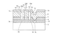
【解決手段】この光起電力装置1は、基板2と、開溝部3cにより分離された基板側電極3aおよび3bと、光電変換ユニット4と、導電性を有する中間層5を介して形成された光電変換ユニット6と、開溝部7dにより分離された背面電極7aおよび7bと、中間層5を切断するように形成された開溝部20bと、開溝部20bに埋め込まれた絶縁部材8と、開溝部20aと開溝部20bとの間の領域に形成された開溝部20cと、開溝部20c内に露出された基板側電極3aの表面に接触するように埋められるとともに、絶縁部材8を跨いで背面電極7bに電気的に接続される接続電極9とを備えている。
【選択図】図1
Description
図1は、本発明の第1実施形態による光起電力装置の構成を示した断面図である。まず、図1を参照して、本発明の第1実施形態による光起電力装置の構成について説明する。

図8は、本発明の第2実施形態による光起電力装置の構成を示した断面図である。図8を参照して、この第2実施形態では、上記第1実施形態とは異なり、基板側電極3aと背面電極7bとがシリコン溶融物22と接続電極23とにより電気的に接続された光起電力装置21について説明する。
2 基板
3 基板側電極
3a 基板側電極(第1基板側電極)
3b 基板側電極(第2基板側電極)
3c 開溝部(第1開溝部)
4 光電変換ユニット(第1光電変換部)
4a、5a、6a、7c、20c 開溝部(第4開溝部)
4b、5b、6b、7d、20a 開溝部(第2開溝部)
4c、5c、6c、7e、20b 開溝部(第3開溝部)
5 中間層
6 光電変換ユニット(第2光電変換部)
7 背面電極
7a 背面電極(第1背面電極)
7b 背面電極(第2背面電極)
8 絶縁部材(第1絶縁部材)
9 接続電極(導電性部材)
10 絶縁部材(第2絶縁部材)
22 シリコン溶融物(溶融部、導電性部材)
23 接続電極(接続部、導電性部材)
Claims (5)
- 絶縁性表面を有する基板と、
前記基板の絶縁性表面上に形成され、第1開溝部により分離された第1基板側電極および第2基板側電極と、
前記第1基板側電極および前記第2基板側電極を覆うように形成された第1光電変換部と、
前記第1光電変換部の表面上に導電性を有する中間層を介して形成された第2光電変換部と、
前記第2光電変換部の表面上に形成され、前記第1基板側電極および前記第2基板側電極にそれぞれ対応する第1背面電極および第2背面電極と、
前記第1背面電極と前記第2背面電極とを電気的に分離するための第2開溝部と、
前記第1開溝部と前記第2開溝部との間の領域において、前記第2背面電極の上面から少なくとも前記中間層を切断するように形成された第3開溝部と、
前記第3開溝部内に、少なくとも前記中間層の切断部を覆うように埋め込まれた第1絶縁部材と、
前記第2開溝部と前記第3開溝部との間の領域において、前記第1基板側電極に電気的に接続されるとともに、前記第3開溝部を跨いで前記第2背面電極に電気的に接続される導電性部材とを備える、光起電力装置。 - 前記第2開溝部と前記第3開溝部との間の領域において、前記第2背面電極、前記第2光電変換部、前記中間層および前記第1光電変換部を貫通するとともに、前記第1基板側電極の表面を露出するように形成された第4開溝部をさらに備え、
前記導電性部材は、前記第4開溝部内に露出された前記第1基板側電極の表面に接触するように前記第4開溝部に埋められるとともに、前記第3開溝部内に埋め込まれた前記第1絶縁部材を跨いで前記第2背面電極に電気的に接続されるように形成されている、請求項1に記載の光起電力装置。 - 前記導電性部材は、前記第2開溝部と前記第3開溝部との間の領域に、前記第2背面電極、前記第2光電変換部、前記中間層および前記第1光電変換部を溶融させることにより得られ、前記第1基板側電極に電気的に接続される導電性を有する溶融部と、前記溶融部と電気的に接続されるとともに、前記第3開溝部内に埋め込まれた前記第1絶縁部材を跨いで前記第2背面電極に電気的に接続されるように形成された接続部とを含む、請求項1に記載の光起電力装置。
- 前記第2開溝部内に埋め込むように形成された第2絶縁部材をさらに備える、請求項1〜3のいずれか1項に記載の光起電力装置。
- 絶縁性表面を有する基板の前記絶縁性表面上に基板側電極を形成する工程と、
前記基板側電極に第1開溝部を形成することによって、前記第1開溝部により分離された第1基板側電極および第2基板側電極を形成する工程と、
前記第1基板側電極および前記第2基板側電極を覆うように第1光電変換部を形成する工程と、
前記第1光電変換部の表面上に導電性を有する中間層を介して第2光電変換部を形成する工程と、
前記第2光電変換部の表面上に背面電極を形成する工程と、
その後、前記背面電極を第1背面電極および第2背面電に分離するための第2開溝部を形成するとともに、前記第1開溝部と前記第2開溝部との間の領域において、前記第2背面電極の上面から少なくとも前記中間層を貫くように第3開溝部を形成する工程と、
前記第3開溝部内に、少なくとも前記中間層の切断部を覆うように第1絶縁部材を形成する工程と、
前記第2開溝部と前記第3開溝部との間の領域において、前記第1基板側電極に電気的に接続されるとともに、前記第3開溝部を跨いで前記第2背面電極に電気的に接続される導電性部材を形成する工程とを備える、光起電力装置の製造方法。
Priority Applications (5)
| Application Number | Priority Date | Filing Date | Title |
|---|---|---|---|
| JP2006046083A JP5081389B2 (ja) | 2006-02-23 | 2006-02-23 | 光起電力装置の製造方法 |
| US11/705,770 US8207441B2 (en) | 2006-02-23 | 2007-02-14 | Photovoltaic apparatus and method of manufacturing the same |
| CN2007100788236A CN101026174B (zh) | 2006-02-23 | 2007-02-15 | 半导体装置及其制造方法 |
| EP07250625A EP1826830A3 (en) | 2006-02-23 | 2007-02-15 | Photovoltaic apparatus and method of manufacturing the same |
| CN2010100033454A CN101794794B (zh) | 2006-02-23 | 2007-02-15 | 光电动势装置 |
Applications Claiming Priority (1)
| Application Number | Priority Date | Filing Date | Title |
|---|---|---|---|
| JP2006046083A JP5081389B2 (ja) | 2006-02-23 | 2006-02-23 | 光起電力装置の製造方法 |
Publications (2)
| Publication Number | Publication Date |
|---|---|
| JP2007227577A true JP2007227577A (ja) | 2007-09-06 |
| JP5081389B2 JP5081389B2 (ja) | 2012-11-28 |
Family
ID=38134845
Family Applications (1)
| Application Number | Title | Priority Date | Filing Date |
|---|---|---|---|
| JP2006046083A Expired - Fee Related JP5081389B2 (ja) | 2006-02-23 | 2006-02-23 | 光起電力装置の製造方法 |
Country Status (4)
| Country | Link |
|---|---|
| US (1) | US8207441B2 (ja) |
| EP (1) | EP1826830A3 (ja) |
| JP (1) | JP5081389B2 (ja) |
| CN (2) | CN101794794B (ja) |
Cited By (7)
| Publication number | Priority date | Publication date | Assignee | Title |
|---|---|---|---|---|
| JP2009158864A (ja) * | 2007-12-27 | 2009-07-16 | Sanyo Electric Co Ltd | 太陽電池モジュール及びその製造方法 |
| JP2010278441A (ja) * | 2009-05-26 | 2010-12-09 | Korea Iron & Steel Co Ltd | 集積型薄膜太陽電池及びその製造方法 |
| KR101173418B1 (ko) | 2011-07-29 | 2012-08-10 | 엘지이노텍 주식회사 | 태양전지 및 이의 제조방법 |
| US8362354B2 (en) | 2007-07-09 | 2013-01-29 | Sanyo Electric Co., Ltd. | Photovoltaic apparatus and method of manufacturing the same |
| WO2013058524A1 (en) * | 2011-10-18 | 2013-04-25 | Lg Innotek Co., Ltd. | Solar cell apparatus and method of fabricating the same |
| WO2013108623A1 (ja) * | 2012-01-18 | 2013-07-25 | 富士フイルム株式会社 | 集積化太陽電池の製造方法 |
| WO2014003442A1 (en) * | 2012-06-28 | 2014-01-03 | Lg Innotek Co., Ltd. | Solar cell and method of fabricating the same |
Families Citing this family (9)
| Publication number | Priority date | Publication date | Assignee | Title |
|---|---|---|---|---|
| KR101120269B1 (ko) * | 2007-08-14 | 2012-03-06 | 미츠비시 쥬고교 가부시키가이샤 | 광전 변환 장치 및 그 제조 방법 |
| CN101803038B (zh) * | 2007-09-18 | 2012-02-29 | 三菱电机株式会社 | 薄膜太阳能电池元件及其制造方法 |
| DE102008006166A1 (de) * | 2008-01-26 | 2009-07-30 | Schott Solar Gmbh | Verfahren zur Herstellung eines photovoltaischen Moduls |
| KR101119235B1 (ko) * | 2008-07-04 | 2012-03-21 | 가부시키가이샤 아루박 | 태양 전지 셀의 제조 방법 및 태양 전지 셀 |
| DE102009022318A1 (de) * | 2009-05-22 | 2010-12-23 | Schott Solar Ag | Verfahren zur Herstellung eines photovoltaischen Moduls |
| KR101166456B1 (ko) * | 2011-05-23 | 2012-07-19 | 김병국 | 태양전지 및 그 제조방법 |
| US20130229777A1 (en) * | 2012-03-01 | 2013-09-05 | Infineon Technologies Ag | Chip arrangements and methods for forming a chip arrangement |
| TWM545367U (zh) * | 2017-02-24 | 2017-07-11 | Nano Bit Tech Co Ltd | 光伏電池裝置、光伏電池及其光伏模組 |
| JP7186785B2 (ja) * | 2019-03-19 | 2022-12-09 | 株式会社東芝 | 光電変換素子および光電変換素子の製造方法 |
Citations (10)
| Publication number | Priority date | Publication date | Assignee | Title |
|---|---|---|---|---|
| JPS63157482A (ja) * | 1986-12-22 | 1988-06-30 | Kanegafuchi Chem Ind Co Ltd | 半導体装置及びその製法 |
| JPH07335924A (ja) * | 1994-06-10 | 1995-12-22 | Siemens Ag | ソーラモジュールの製造方法 |
| JPH0982998A (ja) * | 1995-09-11 | 1997-03-28 | Canon Inc | 光起電力素子アレー及びその製造方法 |
| JPH09129906A (ja) * | 1995-10-30 | 1997-05-16 | Kanegafuchi Chem Ind Co Ltd | 集積化薄膜タンデム太陽電池とその製造方法 |
| JP2000058886A (ja) * | 1998-08-14 | 2000-02-25 | Mitsubishi Heavy Ind Ltd | 太陽電池モジュール及びその製造方法 |
| JP2001274447A (ja) * | 2000-03-23 | 2001-10-05 | Kanegafuchi Chem Ind Co Ltd | 集積型薄膜太陽電池の製造方法 |
| JP2003273383A (ja) * | 2002-03-15 | 2003-09-26 | Sharp Corp | 太陽電池素子およびその製造方法 |
| JP2005038907A (ja) * | 2003-07-15 | 2005-02-10 | Kyocera Corp | 集積型光電変換装置 |
| JP2005093939A (ja) * | 2003-09-19 | 2005-04-07 | Mitsubishi Heavy Ind Ltd | 集積型タンデム接合太陽電池及び集積型タンデム接合太陽電池の製造方法 |
| JP2005101384A (ja) * | 2003-09-26 | 2005-04-14 | Sanyo Electric Co Ltd | 光起電力装置及びその製造方法 |
Family Cites Families (13)
| Publication number | Priority date | Publication date | Assignee | Title |
|---|---|---|---|---|
| US4110122A (en) * | 1976-05-26 | 1978-08-29 | Massachusetts Institute Of Technology | High-intensity, solid-state-solar cell device |
| JPS59201471A (ja) * | 1983-04-29 | 1984-11-15 | Semiconductor Energy Lab Co Ltd | 光電変換半導体装置 |
| JPS61214483A (ja) | 1985-03-19 | 1986-09-24 | Teijin Ltd | 集積型太陽電池の製造方法 |
| US4697041A (en) | 1985-02-15 | 1987-09-29 | Teijin Limited | Integrated solar cells |
| US4675467A (en) * | 1986-04-05 | 1987-06-23 | Chronar Corp. | Directed energy conversion of semiconductor materials |
| US6265652B1 (en) | 1995-06-15 | 2001-07-24 | Kanegafuchi Kagaku Kogyo Kabushiki Kabushiki Kaisha | Integrated thin-film solar battery and method of manufacturing the same |
| JP2002118273A (ja) | 2000-10-05 | 2002-04-19 | Kanegafuchi Chem Ind Co Ltd | 集積型ハイブリッド薄膜光電変換装置 |
| US6632993B2 (en) * | 2000-10-05 | 2003-10-14 | Kaneka Corporation | Photovoltaic module |
| JP2002261308A (ja) | 2001-03-01 | 2002-09-13 | Kanegafuchi Chem Ind Co Ltd | 薄膜光電変換モジュール |
| JP4201241B2 (ja) | 2001-05-17 | 2008-12-24 | 株式会社カネカ | 集積型薄膜光電変換モジュールの作製方法 |
| JP2004095661A (ja) | 2002-08-29 | 2004-03-25 | Sanyo Electric Co Ltd | 光電変換装置およびその製造方法 |
| JP2006013403A (ja) | 2004-06-29 | 2006-01-12 | Sanyo Electric Co Ltd | 太陽電池、太陽電池モジュール、その製造方法およびその修復方法 |
| US7235736B1 (en) | 2006-03-18 | 2007-06-26 | Solyndra, Inc. | Monolithic integration of cylindrical solar cells |
-
2006
- 2006-02-23 JP JP2006046083A patent/JP5081389B2/ja not_active Expired - Fee Related
-
2007
- 2007-02-14 US US11/705,770 patent/US8207441B2/en not_active Expired - Fee Related
- 2007-02-15 CN CN2010100033454A patent/CN101794794B/zh not_active Expired - Fee Related
- 2007-02-15 CN CN2007100788236A patent/CN101026174B/zh not_active Expired - Fee Related
- 2007-02-15 EP EP07250625A patent/EP1826830A3/en not_active Withdrawn
Patent Citations (10)
| Publication number | Priority date | Publication date | Assignee | Title |
|---|---|---|---|---|
| JPS63157482A (ja) * | 1986-12-22 | 1988-06-30 | Kanegafuchi Chem Ind Co Ltd | 半導体装置及びその製法 |
| JPH07335924A (ja) * | 1994-06-10 | 1995-12-22 | Siemens Ag | ソーラモジュールの製造方法 |
| JPH0982998A (ja) * | 1995-09-11 | 1997-03-28 | Canon Inc | 光起電力素子アレー及びその製造方法 |
| JPH09129906A (ja) * | 1995-10-30 | 1997-05-16 | Kanegafuchi Chem Ind Co Ltd | 集積化薄膜タンデム太陽電池とその製造方法 |
| JP2000058886A (ja) * | 1998-08-14 | 2000-02-25 | Mitsubishi Heavy Ind Ltd | 太陽電池モジュール及びその製造方法 |
| JP2001274447A (ja) * | 2000-03-23 | 2001-10-05 | Kanegafuchi Chem Ind Co Ltd | 集積型薄膜太陽電池の製造方法 |
| JP2003273383A (ja) * | 2002-03-15 | 2003-09-26 | Sharp Corp | 太陽電池素子およびその製造方法 |
| JP2005038907A (ja) * | 2003-07-15 | 2005-02-10 | Kyocera Corp | 集積型光電変換装置 |
| JP2005093939A (ja) * | 2003-09-19 | 2005-04-07 | Mitsubishi Heavy Ind Ltd | 集積型タンデム接合太陽電池及び集積型タンデム接合太陽電池の製造方法 |
| JP2005101384A (ja) * | 2003-09-26 | 2005-04-14 | Sanyo Electric Co Ltd | 光起電力装置及びその製造方法 |
Cited By (11)
| Publication number | Priority date | Publication date | Assignee | Title |
|---|---|---|---|---|
| US8362354B2 (en) | 2007-07-09 | 2013-01-29 | Sanyo Electric Co., Ltd. | Photovoltaic apparatus and method of manufacturing the same |
| JP2009158864A (ja) * | 2007-12-27 | 2009-07-16 | Sanyo Electric Co Ltd | 太陽電池モジュール及びその製造方法 |
| JP2010278441A (ja) * | 2009-05-26 | 2010-12-09 | Korea Iron & Steel Co Ltd | 集積型薄膜太陽電池及びその製造方法 |
| KR101173418B1 (ko) | 2011-07-29 | 2012-08-10 | 엘지이노텍 주식회사 | 태양전지 및 이의 제조방법 |
| WO2013019028A3 (en) * | 2011-07-29 | 2013-05-02 | Lg Innotek Co., Ltd. | Solar cell and method of fabricating the same |
| US9818892B2 (en) | 2011-07-29 | 2017-11-14 | Lg Innotek Co., Ltd. | Solar cell and method of fabricating the same |
| WO2013058524A1 (en) * | 2011-10-18 | 2013-04-25 | Lg Innotek Co., Ltd. | Solar cell apparatus and method of fabricating the same |
| KR101283072B1 (ko) * | 2011-10-18 | 2013-07-05 | 엘지이노텍 주식회사 | 태양광 발전장치 및 이의 제조방법 |
| US9559223B2 (en) | 2011-10-18 | 2017-01-31 | Lg Innotek Co., Ltd. | Solar cell apparatus and method of fabricating the same |
| WO2013108623A1 (ja) * | 2012-01-18 | 2013-07-25 | 富士フイルム株式会社 | 集積化太陽電池の製造方法 |
| WO2014003442A1 (en) * | 2012-06-28 | 2014-01-03 | Lg Innotek Co., Ltd. | Solar cell and method of fabricating the same |
Also Published As
| Publication number | Publication date |
|---|---|
| EP1826830A3 (en) | 2010-02-24 |
| CN101794794B (zh) | 2011-12-28 |
| US20070193619A1 (en) | 2007-08-23 |
| JP5081389B2 (ja) | 2012-11-28 |
| US8207441B2 (en) | 2012-06-26 |
| CN101026174A (zh) | 2007-08-29 |
| EP1826830A2 (en) | 2007-08-29 |
| CN101026174B (zh) | 2010-05-26 |
| CN101794794A (zh) | 2010-08-04 |
Similar Documents
| Publication | Publication Date | Title |
|---|---|---|
| JP5081389B2 (ja) | 光起電力装置の製造方法 | |
| JP4703433B2 (ja) | 光起電力装置 | |
| JP4425296B2 (ja) | 光起電力装置 | |
| JP4439492B2 (ja) | カルコパイライト型太陽電池およびその製造方法 | |
| JP4730740B2 (ja) | 太陽電池およびその製造方法 | |
| JP4925724B2 (ja) | 太陽電池およびその製造方法 | |
| EP2439786A2 (en) | Solar photovoltaic device and a production method for the same | |
| JP5220134B2 (ja) | 光電変換セルおよび光電変換モジュール | |
| JP2007317879A (ja) | カルコパイライト型太陽電池およびその製造方法 | |
| JP2007317868A (ja) | カルコパイライト型太陽電池およびその製造方法 | |
| JPWO2010087333A1 (ja) | 光電変換セル、光電変換モジュールおよび光電変換セルの製造方法 | |
| WO2009080640A2 (en) | Method for providing a series connection in a solar cell system | |
| JP4889779B2 (ja) | 光電変換モジュール | |
| JP2009302274A (ja) | 光発電素子、cis系光発電素子の製造方法 | |
| JP2009283982A (ja) | 薄膜太陽電池モジュールの製造方法 | |
| JP2010093308A (ja) | 薄膜太陽電池モジュールの製造方法 | |
| JP2010093309A (ja) | 薄膜太陽電池モジュールの製造方法 | |
| EP2528106A1 (en) | Photovoltaic power generation device and manufacturing method thereof | |
| JPH077840B2 (ja) | 光電変換半導体装置の作製方法 | |
| JP2001111079A (ja) | 光電変換装置の製造方法 | |
| JP2013012670A (ja) | 光電変換モジュールおよびその製造方法 |
Legal Events
| Date | Code | Title | Description |
|---|---|---|---|
| A621 | Written request for application examination |
Free format text: JAPANESE INTERMEDIATE CODE: A621 Effective date: 20080522 |
|
| A977 | Report on retrieval |
Free format text: JAPANESE INTERMEDIATE CODE: A971007 Effective date: 20100915 |
|
| A131 | Notification of reasons for refusal |
Free format text: JAPANESE INTERMEDIATE CODE: A131 Effective date: 20100921 |
|
| A521 | Request for written amendment filed |
Free format text: JAPANESE INTERMEDIATE CODE: A523 Effective date: 20101118 |
|
| A131 | Notification of reasons for refusal |
Free format text: JAPANESE INTERMEDIATE CODE: A131 Effective date: 20110719 |
|
| A521 | Request for written amendment filed |
Free format text: JAPANESE INTERMEDIATE CODE: A523 Effective date: 20110915 |
|
| TRDD | Decision of grant or rejection written | ||
| A01 | Written decision to grant a patent or to grant a registration (utility model) |
Free format text: JAPANESE INTERMEDIATE CODE: A01 Effective date: 20120807 |
|
| A01 | Written decision to grant a patent or to grant a registration (utility model) |
Free format text: JAPANESE INTERMEDIATE CODE: A01 |
|
| A61 | First payment of annual fees (during grant procedure) |
Free format text: JAPANESE INTERMEDIATE CODE: A61 Effective date: 20120903 |
|
| FPAY | Renewal fee payment (event date is renewal date of database) |
Free format text: PAYMENT UNTIL: 20150907 Year of fee payment: 3 |
|
| FPAY | Renewal fee payment (event date is renewal date of database) |
Free format text: PAYMENT UNTIL: 20150907 Year of fee payment: 3 |
|
| LAPS | Cancellation because of no payment of annual fees |