JP2007194511A - 不揮発性半導体記憶装置およびその製造方法 - Google Patents
不揮発性半導体記憶装置およびその製造方法 Download PDFInfo
- Publication number
- JP2007194511A JP2007194511A JP2006013276A JP2006013276A JP2007194511A JP 2007194511 A JP2007194511 A JP 2007194511A JP 2006013276 A JP2006013276 A JP 2006013276A JP 2006013276 A JP2006013276 A JP 2006013276A JP 2007194511 A JP2007194511 A JP 2007194511A
- Authority
- JP
- Japan
- Prior art keywords
- film
- charge retention
- memory device
- charge
- semiconductor memory
- Prior art date
- Legal status (The legal status is an assumption and is not a legal conclusion. Google has not performed a legal analysis and makes no representation as to the accuracy of the status listed.)
- Pending
Links
- 239000004065 semiconductor Substances 0.000 title claims abstract description 75
- 238000000034 method Methods 0.000 title claims description 73
- 238000004519 manufacturing process Methods 0.000 title claims description 24
- 230000014759 maintenance of location Effects 0.000 claims abstract description 108
- 239000000758 substrate Substances 0.000 claims abstract description 63
- 229910052710 silicon Inorganic materials 0.000 claims abstract description 23
- 239000010703 silicon Substances 0.000 claims abstract description 21
- 239000002784 hot electron Substances 0.000 claims abstract description 14
- QGZKDVFQNNGYKY-UHFFFAOYSA-N Ammonia Chemical compound N QGZKDVFQNNGYKY-UHFFFAOYSA-N 0.000 claims description 80
- 239000000203 mixture Substances 0.000 claims description 61
- 238000002347 injection Methods 0.000 claims description 54
- 239000007924 injection Substances 0.000 claims description 54
- 150000004767 nitrides Chemical class 0.000 claims description 53
- 229910021529 ammonia Inorganic materials 0.000 claims description 40
- 238000005036 potential barrier Methods 0.000 claims description 34
- 239000010410 layer Substances 0.000 claims description 29
- BLRPTPMANUNPDV-UHFFFAOYSA-N Silane Chemical compound [SiH4] BLRPTPMANUNPDV-UHFFFAOYSA-N 0.000 claims description 20
- 239000004020 conductor Substances 0.000 claims description 17
- 239000002356 single layer Substances 0.000 claims description 16
- 238000005229 chemical vapour deposition Methods 0.000 claims description 15
- MROCJMGDEKINLD-UHFFFAOYSA-N dichlorosilane Chemical compound Cl[SiH2]Cl MROCJMGDEKINLD-UHFFFAOYSA-N 0.000 claims description 15
- 229910000077 silane Inorganic materials 0.000 claims description 14
- 239000002994 raw material Substances 0.000 claims description 8
- 238000000059 patterning Methods 0.000 claims description 6
- 238000003860 storage Methods 0.000 claims description 6
- 230000004888 barrier function Effects 0.000 claims description 3
- 229910017464 nitrogen compound Inorganic materials 0.000 claims description 3
- 150000002830 nitrogen compounds Chemical class 0.000 claims description 3
- 150000003377 silicon compounds Chemical class 0.000 claims description 3
- 230000015654 memory Effects 0.000 abstract description 157
- 238000002955 isolation Methods 0.000 abstract description 14
- XUIMIQQOPSSXEZ-UHFFFAOYSA-N Silicon Chemical compound [Si] XUIMIQQOPSSXEZ-UHFFFAOYSA-N 0.000 abstract description 10
- VYPSYNLAJGMNEJ-UHFFFAOYSA-N Silicium dioxide Chemical compound O=[Si]=O VYPSYNLAJGMNEJ-UHFFFAOYSA-N 0.000 abstract description 4
- 229910052814 silicon oxide Inorganic materials 0.000 abstract description 3
- 229910052581 Si3N4 Inorganic materials 0.000 abstract description 2
- HQVNEWCFYHHQES-UHFFFAOYSA-N silicon nitride Chemical compound N12[Si]34N5[Si]62N3[Si]51N64 HQVNEWCFYHHQES-UHFFFAOYSA-N 0.000 abstract 1
- 239000010408 film Substances 0.000 description 599
- 239000007789 gas Substances 0.000 description 47
- 238000010586 diagram Methods 0.000 description 20
- 230000004807 localization Effects 0.000 description 18
- 230000006866 deterioration Effects 0.000 description 16
- 230000005684 electric field Effects 0.000 description 16
- 238000009826 distribution Methods 0.000 description 15
- 238000002230 thermal chemical vapour deposition Methods 0.000 description 15
- 239000003990 capacitor Substances 0.000 description 13
- 230000015572 biosynthetic process Effects 0.000 description 11
- 230000003647 oxidation Effects 0.000 description 11
- 238000007254 oxidation reaction Methods 0.000 description 11
- 229910021420 polycrystalline silicon Inorganic materials 0.000 description 9
- 239000000969 carrier Substances 0.000 description 8
- 230000015556 catabolic process Effects 0.000 description 7
- BUMGIEFFCMBQDG-UHFFFAOYSA-N dichlorosilicon Chemical compound Cl[Si]Cl BUMGIEFFCMBQDG-UHFFFAOYSA-N 0.000 description 7
- 238000000206 photolithography Methods 0.000 description 7
- 238000010926 purge Methods 0.000 description 7
- 230000006798 recombination Effects 0.000 description 7
- 238000005215 recombination Methods 0.000 description 7
- GQPLMRYTRLFLPF-UHFFFAOYSA-N Nitrous Oxide Chemical compound [O-][N+]#N GQPLMRYTRLFLPF-UHFFFAOYSA-N 0.000 description 6
- 230000007423 decrease Effects 0.000 description 6
- 238000006731 degradation reaction Methods 0.000 description 6
- 238000009792 diffusion process Methods 0.000 description 6
- 235000012431 wafers Nutrition 0.000 description 6
- IJGRMHOSHXDMSA-UHFFFAOYSA-N Atomic nitrogen Chemical compound N#N IJGRMHOSHXDMSA-UHFFFAOYSA-N 0.000 description 5
- 238000005259 measurement Methods 0.000 description 5
- 239000012528 membrane Substances 0.000 description 5
- 230000001590 oxidative effect Effects 0.000 description 5
- MWUXSHHQAYIFBG-UHFFFAOYSA-N Nitric oxide Chemical compound O=[N] MWUXSHHQAYIFBG-UHFFFAOYSA-N 0.000 description 4
- 238000005530 etching Methods 0.000 description 4
- 230000008901 benefit Effects 0.000 description 3
- 150000001875 compounds Chemical class 0.000 description 3
- 238000000151 deposition Methods 0.000 description 3
- 230000009977 dual effect Effects 0.000 description 3
- 230000000694 effects Effects 0.000 description 3
- 238000000572 ellipsometry Methods 0.000 description 3
- 239000012535 impurity Substances 0.000 description 3
- 238000005468 ion implantation Methods 0.000 description 3
- 238000004518 low pressure chemical vapour deposition Methods 0.000 description 3
- 239000001272 nitrous oxide Substances 0.000 description 3
- 238000005240 physical vapour deposition Methods 0.000 description 3
- 230000005641 tunneling Effects 0.000 description 3
- XKRFYHLGVUSROY-UHFFFAOYSA-N Argon Chemical compound [Ar] XKRFYHLGVUSROY-UHFFFAOYSA-N 0.000 description 2
- ZOXJGFHDIHLPTG-UHFFFAOYSA-N Boron Chemical compound [B] ZOXJGFHDIHLPTG-UHFFFAOYSA-N 0.000 description 2
- OAKJQQAXSVQMHS-UHFFFAOYSA-N Hydrazine Chemical compound NN OAKJQQAXSVQMHS-UHFFFAOYSA-N 0.000 description 2
- 229910008045 Si-Si Inorganic materials 0.000 description 2
- 229910006411 Si—Si Inorganic materials 0.000 description 2
- 230000001133 acceleration Effects 0.000 description 2
- 229910052796 boron Inorganic materials 0.000 description 2
- 230000008030 elimination Effects 0.000 description 2
- 238000003379 elimination reaction Methods 0.000 description 2
- 230000006870 function Effects 0.000 description 2
- 238000002513 implantation Methods 0.000 description 2
- 239000011229 interlayer Substances 0.000 description 2
- 238000012986 modification Methods 0.000 description 2
- 230000004048 modification Effects 0.000 description 2
- 238000005121 nitriding Methods 0.000 description 2
- 229910052757 nitrogen Inorganic materials 0.000 description 2
- 238000005498 polishing Methods 0.000 description 2
- 238000004544 sputter deposition Methods 0.000 description 2
- 239000000126 substance Substances 0.000 description 2
- VXEGSRKPIUDPQT-UHFFFAOYSA-N 4-[4-(4-methoxyphenyl)piperazin-1-yl]aniline Chemical compound C1=CC(OC)=CC=C1N1CCN(C=2C=CC(N)=CC=2)CC1 VXEGSRKPIUDPQT-UHFFFAOYSA-N 0.000 description 1
- UFHFLCQGNIYNRP-UHFFFAOYSA-N Hydrogen Chemical compound [H][H] UFHFLCQGNIYNRP-UHFFFAOYSA-N 0.000 description 1
- WYQGNUUOBJVAKM-UHFFFAOYSA-N N.Cl[SiH2]Cl Chemical compound N.Cl[SiH2]Cl WYQGNUUOBJVAKM-UHFFFAOYSA-N 0.000 description 1
- CBENFWSGALASAD-UHFFFAOYSA-N Ozone Chemical compound [O-][O+]=O CBENFWSGALASAD-UHFFFAOYSA-N 0.000 description 1
- 229910003902 SiCl 4 Inorganic materials 0.000 description 1
- 229910052786 argon Inorganic materials 0.000 description 1
- QVGXLLKOCUKJST-UHFFFAOYSA-N atomic oxygen Chemical compound [O] QVGXLLKOCUKJST-UHFFFAOYSA-N 0.000 description 1
- 230000006399 behavior Effects 0.000 description 1
- 239000000470 constituent Substances 0.000 description 1
- 229910021419 crystalline silicon Inorganic materials 0.000 description 1
- 230000003247 decreasing effect Effects 0.000 description 1
- 230000007547 defect Effects 0.000 description 1
- 230000008021 deposition Effects 0.000 description 1
- 230000002542 deteriorative effect Effects 0.000 description 1
- PZPGRFITIJYNEJ-UHFFFAOYSA-N disilane Chemical compound [SiH3][SiH3] PZPGRFITIJYNEJ-UHFFFAOYSA-N 0.000 description 1
- 230000005669 field effect Effects 0.000 description 1
- 229910052736 halogen Inorganic materials 0.000 description 1
- 150000002367 halogens Chemical class 0.000 description 1
- 238000004050 hot filament vapor deposition Methods 0.000 description 1
- 239000001257 hydrogen Substances 0.000 description 1
- 229910052739 hydrogen Inorganic materials 0.000 description 1
- 239000012212 insulator Substances 0.000 description 1
- 239000002184 metal Substances 0.000 description 1
- 239000001301 oxygen Substances 0.000 description 1
- 229910052760 oxygen Inorganic materials 0.000 description 1
- 238000005268 plasma chemical vapour deposition Methods 0.000 description 1
- 230000008569 process Effects 0.000 description 1
- 239000005049 silicon tetrachloride Substances 0.000 description 1
- 239000000243 solution Substances 0.000 description 1
- 239000010409 thin film Substances 0.000 description 1
- 238000003949 trap density measurement Methods 0.000 description 1
- XLYOFNOQVPJJNP-UHFFFAOYSA-N water Chemical compound O XLYOFNOQVPJJNP-UHFFFAOYSA-N 0.000 description 1
Images


Classifications
-
- H—ELECTRICITY
- H01—ELECTRIC ELEMENTS
- H01L—SEMICONDUCTOR DEVICES NOT COVERED BY CLASS H10
- H01L29/00—Semiconductor devices adapted for rectifying, amplifying, oscillating or switching, or capacitors or resistors with at least one potential-jump barrier or surface barrier, e.g. PN junction depletion layer or carrier concentration layer; Details of semiconductor bodies or of electrodes thereof ; Multistep manufacturing processes therefor
- H01L29/40—Electrodes ; Multistep manufacturing processes therefor
- H01L29/41—Electrodes ; Multistep manufacturing processes therefor characterised by their shape, relative sizes or dispositions
- H01L29/423—Electrodes ; Multistep manufacturing processes therefor characterised by their shape, relative sizes or dispositions not carrying the current to be rectified, amplified or switched
- H01L29/42312—Gate electrodes for field effect devices
- H01L29/42316—Gate electrodes for field effect devices for field-effect transistors
- H01L29/4232—Gate electrodes for field effect devices for field-effect transistors with insulated gate
- H01L29/4234—Gate electrodes for transistors with charge trapping gate insulator
- H01L29/42344—Gate electrodes for transistors with charge trapping gate insulator with at least one additional gate, e.g. program gate, erase gate or select gate
-
- H—ELECTRICITY
- H01—ELECTRIC ELEMENTS
- H01L—SEMICONDUCTOR DEVICES NOT COVERED BY CLASS H10
- H01L29/00—Semiconductor devices adapted for rectifying, amplifying, oscillating or switching, or capacitors or resistors with at least one potential-jump barrier or surface barrier, e.g. PN junction depletion layer or carrier concentration layer; Details of semiconductor bodies or of electrodes thereof ; Multistep manufacturing processes therefor
- H01L29/40—Electrodes ; Multistep manufacturing processes therefor
- H01L29/43—Electrodes ; Multistep manufacturing processes therefor characterised by the materials of which they are formed
- H01L29/49—Metal-insulator-semiconductor electrodes, e.g. gates of MOSFET
- H01L29/51—Insulating materials associated therewith
- H01L29/511—Insulating materials associated therewith with a compositional variation, e.g. multilayer structures
- H01L29/512—Insulating materials associated therewith with a compositional variation, e.g. multilayer structures the variation being parallel to the channel plane
-
- H—ELECTRICITY
- H01—ELECTRIC ELEMENTS
- H01L—SEMICONDUCTOR DEVICES NOT COVERED BY CLASS H10
- H01L29/00—Semiconductor devices adapted for rectifying, amplifying, oscillating or switching, or capacitors or resistors with at least one potential-jump barrier or surface barrier, e.g. PN junction depletion layer or carrier concentration layer; Details of semiconductor bodies or of electrodes thereof ; Multistep manufacturing processes therefor
- H01L29/40—Electrodes ; Multistep manufacturing processes therefor
- H01L29/43—Electrodes ; Multistep manufacturing processes therefor characterised by the materials of which they are formed
- H01L29/49—Metal-insulator-semiconductor electrodes, e.g. gates of MOSFET
- H01L29/51—Insulating materials associated therewith
- H01L29/511—Insulating materials associated therewith with a compositional variation, e.g. multilayer structures
- H01L29/513—Insulating materials associated therewith with a compositional variation, e.g. multilayer structures the variation being perpendicular to the channel plane
-
- H—ELECTRICITY
- H01—ELECTRIC ELEMENTS
- H01L—SEMICONDUCTOR DEVICES NOT COVERED BY CLASS H10
- H01L29/00—Semiconductor devices adapted for rectifying, amplifying, oscillating or switching, or capacitors or resistors with at least one potential-jump barrier or surface barrier, e.g. PN junction depletion layer or carrier concentration layer; Details of semiconductor bodies or of electrodes thereof ; Multistep manufacturing processes therefor
- H01L29/66—Types of semiconductor device ; Multistep manufacturing processes therefor
- H01L29/68—Types of semiconductor device ; Multistep manufacturing processes therefor controllable by only the electric current supplied, or only the electric potential applied, to an electrode which does not carry the current to be rectified, amplified or switched
- H01L29/76—Unipolar devices, e.g. field effect transistors
- H01L29/772—Field effect transistors
- H01L29/78—Field effect transistors with field effect produced by an insulated gate
- H01L29/792—Field effect transistors with field effect produced by an insulated gate with charge trapping gate insulator, e.g. MNOS-memory transistors
-
- Y—GENERAL TAGGING OF NEW TECHNOLOGICAL DEVELOPMENTS; GENERAL TAGGING OF CROSS-SECTIONAL TECHNOLOGIES SPANNING OVER SEVERAL SECTIONS OF THE IPC; TECHNICAL SUBJECTS COVERED BY FORMER USPC CROSS-REFERENCE ART COLLECTIONS [XRACs] AND DIGESTS
- Y10—TECHNICAL SUBJECTS COVERED BY FORMER USPC
- Y10S—TECHNICAL SUBJECTS COVERED BY FORMER USPC CROSS-REFERENCE ART COLLECTIONS [XRACs] AND DIGESTS
- Y10S438/00—Semiconductor device manufacturing: process
- Y10S438/954—Making oxide-nitride-oxide device
Abstract
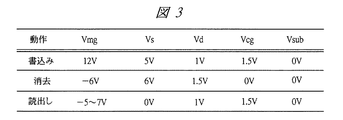
【解決手段】電子により書込み動作を行ない、正孔による消去動作を行なう不揮発性メモリセルは、Si基板上に設けたp型ウェル領域101、素子分離領域102、ソース領域109、ドレイン領域110を有している。ソース領域109とドレイン領域110の間には、ゲート絶縁膜103を介してコントロールゲート電極104が形成されている。コントロールゲート電極104の左側の側壁には、ボトムSi酸化膜105、電荷保持膜106、トップSi酸化膜107およびメモリゲート電極108が形成されている。ここで、化学量論的にシリコンを過剰に含むSi窒化膜から電荷保持膜106を形成する。
【選択図】図1
Description
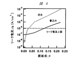
図1〜図14を用いて本発明の実施の形態1を詳細に説明する。図1は、本発明の実施の形態1である不揮発性メモリセルの断面図を示す図である。実際には図の上層に配線が存在するが本図では省略する。図2は、本実施の形態1で作成した試料を示す。本実施の形態1では、図2に示すように電荷保持膜に化学量論比のSi3N4膜を用いた試料Aと、化学量論的にシリコン原子(Si)が過剰に導入されているSRN膜を用いた試料B、Cを作製した例を挙げる。試料Bと試料Cは、SRN膜の組成が異なっており、試料Cの方がSiをより過剰に含んだSRN膜である。本実施の形態1では、電荷保持膜以外の膜構成および試料A〜Cの製造プロセスは全て同じとしている。すなわち、試料A〜Cに対応する不揮発性メモリセルはすべて図1のような構成をしており、電荷保持膜の組成だけが異なっている。図2を見てわかるように、化学量論的なSi3N4膜(試料A)の屈折率は、約2であり、化学量論的にシリコンを過剰に含む割合が多くなるほど(xが大きくなるほど)屈折率が大きくなっていることがわかる。したがって、電荷保持膜の組成を特定するには、屈折率を測定すればよいことがわかる。屈折率の測定方法は、例えばエリプソメトリ法を使用することで測定できる。図2に示す屈折率は、エリプソメトリ法を使用して測定したものであり、He−Neレーザ(波長633nm)を用いている。このように屈折率を測定することにより、電荷保持膜の組成xを特定することができる。組成xについては発明を実施するための最良の形態の項の始めで説明した定義に基づいている。
また、本実施の形態1では、電荷保持膜106であるSRN膜の形成方法として、モノシラン(SiH4)とアンモニア(NH3)を原料ガスとする熱CVD法の例を示したが、本実施の形態1は原料ガスの種類で限定されるものではなく、Siの供給源(Si化合物)としてモノシラン(SiH4)、ジシラン(Si2H2)、ジクロルシラン(SiH2Cl2)等の水素Si化合物、四塩化シリコン(SiCl4)や六塩化シリコン等のハロゲンSi化合物を使用することができる。また、窒素の供給源として、アンモニア(NH3)の他にヒドラジン(N2H2)などを用いることも無論可能である。その成膜方法としては、プラズマCVD法や触媒CVD法等の他のCVD法を用いても良い。また、スパッタリング(PVD法)を用いてSRN膜を形成してもよい。例えば、Siをターゲットとし窒化性の雰囲気中でスパッタリングを行い、SRN膜を形成する方法などが使用できる。
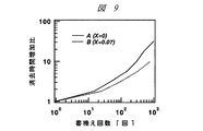
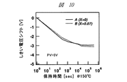
図15〜24を用いて本発明の実施の形態2を詳細に説明する。本発明の実施の形態2である不揮発性メモリセルは、前記実施の形態1の図1に示した構造と基本的には同じであり、電荷保持膜106の構成とSRN膜の組成だけが異なっている。
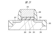
次に、図25〜27を用いて本発明の実施の形態3を説明する。本発明の実施の形態3である不揮発性メモリセルは、図25に示したようにメモリトランジスタ1つで構成された不揮発性メモリであるが、基本的には前記実施の形態1で示したスプリットゲート型不揮発性メモリセルの、メモリトランジスタ領域とほぼ同じ構造である。実際には図25の上層には配線が存在するが本図でも省略している。
102 素子分離領域
103 ゲート絶縁膜
104 コントロールゲート電極
105 ボトムSi酸化膜
106 電荷保持膜
106a SRN膜
106b Si3N4膜
107 トップSi酸化膜
108 メモリゲート電極
109 ソース領域
110 ドレイン領域
111 サイドウォール
201 p型ウェル領域
202 素子分離領域
203 ボトムSi酸化膜
204 電荷保持膜
205 トップSi酸化膜
206 ゲート電極
207 ドレイン領域
208 ソース領域
209 サイドウォール
301 Si基板
302 素子分離領域
303 ゲート絶縁膜
304 コントロールゲート電極
305 Si酸化膜
306 Si窒化膜
307 Si酸化膜
308 メモリゲート電極
309 ソース領域
310 ドレイン領域
Claims (18)
- (a)半導体基板中に形成された第1および第2半導体領域と、
(b)前記第1および第2半導体領域間上の前記半導体基板の上部に形成された第1導電体および第2導電体と、
(c)前記第1導電体と前記半導体基板との間に形成された第1絶縁膜と、
(d)前記第2導電体と前記半導体基板との間に形成された第2絶縁膜とを備え、
(e)前記第2絶縁膜は、前記半導体基板上に形成された第1の電位障壁膜と、前記第1の電位障壁膜の上部に形成された電荷保持膜と、前記電荷保持膜の上部に形成された第2の電位障壁膜よりなり、
前記電荷保持膜に電子を注入することで情報の書込みを行い、正孔を注入することで情報の消去を行う不揮発性半導体記憶装置であって、
前記電荷保持膜は、化学量論的にシリコンを過剰に含むSi窒化膜を有することを特徴とする不揮発性半導体記憶装置。 - 前記電荷保持膜は、化学量論的にシリコンを過剰に含むSi窒化膜よりなる単層膜であることを特徴とする請求項1記載の不揮発性半導体記憶装置。
- 前記電荷保持膜は、化学量論的にシリコンを過剰に含むSi窒化膜と、化学量論的な組成のSi窒化膜との積層膜であることを特徴とする請求項1記載の不揮発性半導体記憶装置。
- 前記電荷保持膜は、化学量論的な組成のSi3N4膜よりもシリコンを過剰に含むSi窒化膜を有することを特徴とする請求項1記載の不揮発性半導体記憶装置。
- (a)半導体基板中に形成された第1および第2半導体領域と、
(b)前記第1および第2半導体領域間上の前記半導体基板の上部に形成された導電体と、
(c)前記導電体と前記半導体基板との間に形成された絶縁膜とを備え、
(d)前記絶縁膜は、前記半導体基板上に形成された第1の電位障壁膜と、前記第1の電位障壁膜の上部に形成された電荷保持膜と、前記電荷保持膜の上部に形成された第2の電位障壁膜よりなり、
前記電荷保持膜に電子を注入することで情報の書込みを行い、正孔を注入することで情報の消去を行う不揮発性半導体記憶装置であって、
前記電荷保持膜は、化学量論的にSiを過剰に含むSi窒化膜を有することを特徴とする不揮発性半導体記憶装置。 - 前記電荷保持膜は、化学量論的にシリコンを過剰に含むSi窒化膜よりなる単層膜であることを特徴とする請求項5記載の不揮発性半導体記憶装置。
- 前記電荷保持膜は、化学量論的にシリコンを過剰に含むSi窒化膜と、化学量論的な組成のSi窒化膜との積層膜であることを特徴とする請求項5記載の不揮発性半導体記憶装置。
- 前記電荷保持膜は、化学量論的な組成のSi3N4膜よりもシリコンを過剰に含むSi窒化膜を有することを特徴とする請求項5記載の不揮発性半導体記憶装置。
- 前記電荷保持膜への電子および正孔の注入に、前記半導体基板中で発生し、前記第1の電位障壁膜の障壁ポテンシャルを超えるエネルギーを有するホットエレクトロンおよびホットホールを用いることを特徴とする請求項1記載の不揮発性半導体記憶装置。
- 前記電荷保持膜は、化学量論的な組成であるSi窒化膜の組成ばらつきを超えた範囲でシリコンを過剰に含んでいることを特徴とする請求項1記載の不揮発性半導体記憶装置。
- 前記電荷保持膜は、化学量論的にシリコンを過剰に含むSi窒化膜と、化学量論的な組成のSi窒化膜との2層膜あるいは3層膜であることを特徴とする請求項3記載の不揮発性半導体記憶装置。
- 前記電荷保持膜は、堆積膜であることを特徴とする請求項1記載の不揮発性半導体記憶装置。
- 電荷を保持する電荷保持膜に電子を注入することで情報の書込みを行い、正孔を注入することで情報の消去を行う不揮発性半導体記憶装置の製造方法であって、
(a)半導体基板上に第1の電位障壁膜を形成する工程と、
(b)前記第1の電位障壁膜上に電荷保持膜を形成する工程と、
(c)前記電荷保持膜上に第2の電位障壁膜を形成する工程と、
(d)前記第2の電位障壁膜上に導電体膜を形成する工程と、
(e)前記第1の電位障壁膜、前記電荷保持膜、前記第2の電位障壁膜および前記導電体膜をパターニングする工程と、
(f)前記半導体基板中に第1および第2半導体領域を形成する工程とを備え、
前記電荷保持膜は、化学量論的にシリコンを過剰に含むSi窒化膜を有することを特徴とする不揮発性半導体記憶装置の製造方法。 - 前記電荷保持膜は、化学量論的にシリコンを過剰に含むSi窒化膜よりなる単層膜であることを特徴とする請求項13記載の不揮発性半導体記憶装置の製造方法。
- 前記電荷保持膜は、化学量論的にシリコンを過剰に含むSi窒化膜と、化学量論的な組成のSi窒化膜との積層膜であることを特徴とする請求項13記載の不揮発性半導体記憶装置の製造方法。
- 前記電荷保持膜は、シリコン化合物と窒素化合物を原料とする化学気相成長法で形成することを特徴とする請求項13記載の不揮発性半導体記憶装置の製造方法。
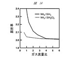
- 前記電荷保持膜は、ジクロルシランとアンモニアを原料とする化学気相成長法で形成し、前記ジクロルシランに対する前記アンモニアの流量比が1以下である条件で形成することを特徴とする請求項16記載の不揮発性半導体記憶装置の製造方法。
- 前記電荷保持膜は、シランとアンモニアを原料とする化学気相成長法で形成し、前記シランに対する前記アンモニアの流量比が4以下である条件で形成することを特徴とする請求項16記載の不揮発性半導体記憶装置の製造方法。
Priority Applications (2)
| Application Number | Priority Date | Filing Date | Title |
|---|---|---|---|
| JP2006013276A JP2007194511A (ja) | 2006-01-23 | 2006-01-23 | 不揮発性半導体記憶装置およびその製造方法 |
| US11/639,134 US8125012B2 (en) | 2006-01-23 | 2006-12-15 | Non-volatile memory device with a silicon nitride charge holding film having an excess of silicon |
Applications Claiming Priority (1)
| Application Number | Priority Date | Filing Date | Title |
|---|---|---|---|
| JP2006013276A JP2007194511A (ja) | 2006-01-23 | 2006-01-23 | 不揮発性半導体記憶装置およびその製造方法 |
Publications (1)
| Publication Number | Publication Date |
|---|---|
| JP2007194511A true JP2007194511A (ja) | 2007-08-02 |
Family
ID=38284690
Family Applications (1)
| Application Number | Title | Priority Date | Filing Date |
|---|---|---|---|
| JP2006013276A Pending JP2007194511A (ja) | 2006-01-23 | 2006-01-23 | 不揮発性半導体記憶装置およびその製造方法 |
Country Status (2)
| Country | Link |
|---|---|
| US (1) | US8125012B2 (ja) |
| JP (1) | JP2007194511A (ja) |
Cited By (1)
| Publication number | Priority date | Publication date | Assignee | Title |
|---|---|---|---|---|
| WO2012014992A1 (ja) * | 2010-07-30 | 2012-02-02 | 学校法人東海大学 | 不揮発性半導体メモリ装置及びその製造方法、並びに電荷蓄積膜 |
Families Citing this family (16)
| Publication number | Priority date | Publication date | Assignee | Title |
|---|---|---|---|---|
| US8320191B2 (en) | 2007-08-30 | 2012-11-27 | Infineon Technologies Ag | Memory cell arrangement, method for controlling a memory cell, memory array and electronic device |
| US7602067B2 (en) * | 2007-12-17 | 2009-10-13 | Spansion Llc | Hetero-structure variable silicon rich nitride for multiple level memory flash memory device |
| JP2009224425A (ja) * | 2008-03-14 | 2009-10-01 | Renesas Technology Corp | 不揮発性半導体記憶装置の製造方法および不揮発性半導体記憶装置 |
| CN103066074A (zh) * | 2011-10-21 | 2013-04-24 | 华东师范大学 | 一种具有双层电介质电荷捕获层的dc-sonos存储器及其制备方法 |
| US9966477B2 (en) | 2012-12-14 | 2018-05-08 | Cypress Semiconductor Corporation | Charge trapping split gate device and method of fabricating same |
| US8836006B2 (en) | 2012-12-14 | 2014-09-16 | Spansion Llc | Integrated circuits with non-volatile memory and methods for manufacture |
| US8822289B2 (en) | 2012-12-14 | 2014-09-02 | Spansion Llc | High voltage gate formation |
| US10014380B2 (en) | 2012-12-14 | 2018-07-03 | Cypress Semiconductor Corporation | Memory first process flow and device |
| US20140167142A1 (en) | 2012-12-14 | 2014-06-19 | Spansion Llc | Use Disposable Gate Cap to Form Transistors, and Split Gate Charge Trapping Memory Cells |
| US20140167220A1 (en) | 2012-12-14 | 2014-06-19 | Spansion Llc | Three dimensional capacitor |
| US9368606B2 (en) | 2012-12-14 | 2016-06-14 | Cypress Semiconductor Corporation | Memory first process flow and device |
| US9209197B2 (en) | 2012-12-14 | 2015-12-08 | Cypress Semiconductor Corporation | Memory gate landing pad made from dummy features |
| US8816438B2 (en) | 2012-12-14 | 2014-08-26 | Spansion Llc | Process charging protection for split gate charge trapping flash |
| US20140167141A1 (en) | 2012-12-14 | 2014-06-19 | Spansion Llc | Charge Trapping Split Gate Embedded Flash Memory and Associated Methods |
| US20140210012A1 (en) | 2013-01-31 | 2014-07-31 | Spansion Llc | Manufacturing of FET Devices Having Lightly Doped Drain and Source Regions |
| KR20140121614A (ko) | 2013-04-08 | 2014-10-16 | 에스케이하이닉스 주식회사 | 비휘발성 메모리 장치 |
Citations (6)
| Publication number | Priority date | Publication date | Assignee | Title |
|---|---|---|---|---|
| JPS5834978A (ja) * | 1981-08-26 | 1983-03-01 | Matsushita Electronics Corp | 半導体記憶装置 |
| JPS6486562A (en) * | 1987-07-31 | 1989-03-31 | Agency Ind Science Techn | Nonvolatile semiconductor memory |
| JPH05145078A (ja) * | 1991-11-22 | 1993-06-11 | Kawasaki Steel Corp | 半導体不揮発性記憶素子とその製造方法 |
| JP2004186452A (ja) * | 2002-12-04 | 2004-07-02 | Renesas Technology Corp | 不揮発性半導体記憶装置およびその製造方法 |
| JP2004363513A (ja) * | 2003-06-09 | 2004-12-24 | Seiko Epson Corp | 半導体記憶装置およびその製造方法 |
| JP2005039138A (ja) * | 2003-07-18 | 2005-02-10 | Nippon Telegr & Teleph Corp <Ntt> | 不揮発性半導体記憶装置 |
Family Cites Families (12)
| Publication number | Priority date | Publication date | Assignee | Title |
|---|---|---|---|---|
| JPH05110114A (ja) | 1991-10-17 | 1993-04-30 | Rohm Co Ltd | 不揮発性半導体記憶素子 |
| JPH05343694A (ja) | 1992-06-05 | 1993-12-24 | Citizen Watch Co Ltd | 半導体不揮発性記憶素子の製造方法 |
| US5969383A (en) * | 1997-06-16 | 1999-10-19 | Motorola, Inc. | Split-gate memory device and method for accessing the same |
| US6368919B2 (en) * | 1999-01-19 | 2002-04-09 | Micron Technology, Inc. | Method and composite for decreasing charge leakage |
| US6465306B1 (en) * | 2000-11-28 | 2002-10-15 | Advanced Micro Devices, Inc. | Simultaneous formation of charge storage and bitline to wordline isolation |
| US6642573B1 (en) * | 2002-03-13 | 2003-11-04 | Advanced Micro Devices, Inc. | Use of high-K dielectric material in modified ONO structure for semiconductor devices |
| US7012299B2 (en) * | 2003-09-23 | 2006-03-14 | Matrix Semiconductors, Inc. | Storage layer optimization of a nonvolatile memory device |
| JP4546117B2 (ja) * | 2004-03-10 | 2010-09-15 | ルネサスエレクトロニクス株式会社 | 不揮発性半導体記憶装置 |
| JP4928773B2 (ja) * | 2004-12-10 | 2012-05-09 | 株式会社東芝 | 半導体装置 |
| US7612403B2 (en) * | 2005-05-17 | 2009-11-03 | Micron Technology, Inc. | Low power non-volatile memory and gate stack |
| KR100672829B1 (ko) * | 2005-08-31 | 2007-01-22 | 삼성전자주식회사 | 전하 트랩 절연체의 제조 방법 및 소노스 타입의 비휘발성메모리 장치의 제조방법 |
| US7531411B2 (en) * | 2005-10-12 | 2009-05-12 | Macronix International Co., Ltd. | Apparatus and method for a non-volatile memory structure comprising a multi-layer silicon-rich, silicon nitride trapping layer |
-
2006
- 2006-01-23 JP JP2006013276A patent/JP2007194511A/ja active Pending
- 2006-12-15 US US11/639,134 patent/US8125012B2/en active Active
Patent Citations (6)
| Publication number | Priority date | Publication date | Assignee | Title |
|---|---|---|---|---|
| JPS5834978A (ja) * | 1981-08-26 | 1983-03-01 | Matsushita Electronics Corp | 半導体記憶装置 |
| JPS6486562A (en) * | 1987-07-31 | 1989-03-31 | Agency Ind Science Techn | Nonvolatile semiconductor memory |
| JPH05145078A (ja) * | 1991-11-22 | 1993-06-11 | Kawasaki Steel Corp | 半導体不揮発性記憶素子とその製造方法 |
| JP2004186452A (ja) * | 2002-12-04 | 2004-07-02 | Renesas Technology Corp | 不揮発性半導体記憶装置およびその製造方法 |
| JP2004363513A (ja) * | 2003-06-09 | 2004-12-24 | Seiko Epson Corp | 半導体記憶装置およびその製造方法 |
| JP2005039138A (ja) * | 2003-07-18 | 2005-02-10 | Nippon Telegr & Teleph Corp <Ntt> | 不揮発性半導体記憶装置 |
Cited By (2)
| Publication number | Priority date | Publication date | Assignee | Title |
|---|---|---|---|---|
| WO2012014992A1 (ja) * | 2010-07-30 | 2012-02-02 | 学校法人東海大学 | 不揮発性半導体メモリ装置及びその製造方法、並びに電荷蓄積膜 |
| JPWO2012014992A1 (ja) * | 2010-07-30 | 2013-09-12 | 学校法人東海大学 | 不揮発性半導体メモリ装置及びその製造方法、並びに電荷蓄積膜 |
Also Published As
| Publication number | Publication date |
|---|---|
| US20070170495A1 (en) | 2007-07-26 |
| US8125012B2 (en) | 2012-02-28 |
Similar Documents
| Publication | Publication Date | Title |
|---|---|---|
| JP2007194511A (ja) | 不揮発性半導体記憶装置およびその製造方法 | |
| KR100890040B1 (ko) | 전하트랩층을 갖는 불휘발성 메모리소자 및 그 제조방법 | |
| US8343840B2 (en) | Blocking dielectric engineered charge trapping memory cell with high speed erase | |
| CN107408558B (zh) | 具有高k电荷俘获层的存储器单元 | |
| US8254175B2 (en) | Semiconductor device and method of manufacturing the same | |
| US10229922B2 (en) | Methods of forming memory devices with isolation structures | |
| US8193577B2 (en) | Nonvolatile semiconductor memory device | |
| JP5336872B2 (ja) | 不揮発性半導体記憶装置及びその製造方法 | |
| CN107408498B (zh) | 形成具有高k电荷俘获层的方法 | |
| JP2007043147A (ja) | 原子層蒸着工程を用いたシリコンリッチナノクリスタル構造物の形成方法及びこれを用いた不揮発性半導体装置の製造方法 | |
| KR101033221B1 (ko) | 전하트랩층을 갖는 불휘발성 메모리소자 및 그 제조방법 | |
| JP2008277530A (ja) | 不揮発性半導体記憶装置 | |
| US20070269972A1 (en) | Method of manufacturing a semiconductor device | |
| US20080093646A1 (en) | Non-volatile memory device and method for fabricating the same | |
| KR100819003B1 (ko) | 비휘발성 메모리 소자 제조 방법 | |
| US20150349143A1 (en) | Semiconductor device and method of manufacturing the same | |
| KR100695820B1 (ko) | 비휘발성 반도체 장치 및 그 제조 방법 | |
| CN106024889A (zh) | 半导体器件及其制造方法 | |
| JP2002261175A (ja) | 不揮発性半導体記憶装置およびその製造方法 | |
| JP2002289708A (ja) | 不揮発性半導体記憶装置およびその製造方法 | |
| TW200924172A (en) | Nonvolatile semiconductor storage device and manufacturing method thereof | |
| JP2006196643A (ja) | 不揮発性半導体記憶装置 | |
| KR100695140B1 (ko) | 실리콘 리치 산화막을 포함하는 메모리 소자의 제조 방법 | |
| US8723248B2 (en) | Nonvolatile semiconductor storage device | |
| KR100722776B1 (ko) | 원자층 증착 공정을 이용한 실리콘 리치 나노-크리스탈구조물의 형성 방법 및 이를 이용한 불휘발성 반도체장치의 제조 방법 |
Legal Events
| Date | Code | Title | Description |
|---|---|---|---|
| A621 | Written request for application examination |
Free format text: JAPANESE INTERMEDIATE CODE: A621 Effective date: 20080624 |
|
| A977 | Report on retrieval |
Free format text: JAPANESE INTERMEDIATE CODE: A971007 Effective date: 20100412 |
|
| A711 | Notification of change in applicant |
Free format text: JAPANESE INTERMEDIATE CODE: A712 Effective date: 20100528 |
|
| A131 | Notification of reasons for refusal |
Free format text: JAPANESE INTERMEDIATE CODE: A131 Effective date: 20111122 |
|
| A02 | Decision of refusal |
Free format text: JAPANESE INTERMEDIATE CODE: A02 Effective date: 20120410 |