JP2007194511A - Non-volatile semiconductor memory device and method for manufacturing the same - Google Patents
Non-volatile semiconductor memory device and method for manufacturing the same Download PDFInfo
- Publication number
- JP2007194511A JP2007194511A JP2006013276A JP2006013276A JP2007194511A JP 2007194511 A JP2007194511 A JP 2007194511A JP 2006013276 A JP2006013276 A JP 2006013276A JP 2006013276 A JP2006013276 A JP 2006013276A JP 2007194511 A JP2007194511 A JP 2007194511A
- Authority
- JP
- Japan
- Prior art keywords
- film
- charge retention
- memory device
- charge
- semiconductor memory
- Prior art date
- Legal status (The legal status is an assumption and is not a legal conclusion. Google has not performed a legal analysis and makes no representation as to the accuracy of the status listed.)
- Pending
Links
- 239000004065 semiconductor Substances 0.000 title claims abstract description 75
- 238000000034 method Methods 0.000 title claims description 73
- 238000004519 manufacturing process Methods 0.000 title claims description 24
- 230000014759 maintenance of location Effects 0.000 claims abstract description 108
- 239000000758 substrate Substances 0.000 claims abstract description 63
- 229910052710 silicon Inorganic materials 0.000 claims abstract description 23
- 239000010703 silicon Substances 0.000 claims abstract description 21
- 239000002784 hot electron Substances 0.000 claims abstract description 14
- QGZKDVFQNNGYKY-UHFFFAOYSA-N Ammonia Chemical compound N QGZKDVFQNNGYKY-UHFFFAOYSA-N 0.000 claims description 80
- 239000000203 mixture Substances 0.000 claims description 61
- 238000002347 injection Methods 0.000 claims description 54
- 239000007924 injection Substances 0.000 claims description 54
- 150000004767 nitrides Chemical class 0.000 claims description 53
- 229910021529 ammonia Inorganic materials 0.000 claims description 40
- 238000005036 potential barrier Methods 0.000 claims description 34
- 239000010410 layer Substances 0.000 claims description 29
- BLRPTPMANUNPDV-UHFFFAOYSA-N Silane Chemical compound [SiH4] BLRPTPMANUNPDV-UHFFFAOYSA-N 0.000 claims description 20
- 239000004020 conductor Substances 0.000 claims description 17
- 239000002356 single layer Substances 0.000 claims description 16
- 238000005229 chemical vapour deposition Methods 0.000 claims description 15
- MROCJMGDEKINLD-UHFFFAOYSA-N dichlorosilane Chemical compound Cl[SiH2]Cl MROCJMGDEKINLD-UHFFFAOYSA-N 0.000 claims description 15
- 229910000077 silane Inorganic materials 0.000 claims description 14
- 239000002994 raw material Substances 0.000 claims description 8
- 238000000059 patterning Methods 0.000 claims description 6
- 238000003860 storage Methods 0.000 claims description 6
- 230000004888 barrier function Effects 0.000 claims description 3
- 229910017464 nitrogen compound Inorganic materials 0.000 claims description 3
- 150000002830 nitrogen compounds Chemical class 0.000 claims description 3
- 150000003377 silicon compounds Chemical class 0.000 claims description 3
- 230000015654 memory Effects 0.000 abstract description 157
- 238000002955 isolation Methods 0.000 abstract description 14
- XUIMIQQOPSSXEZ-UHFFFAOYSA-N Silicon Chemical compound [Si] XUIMIQQOPSSXEZ-UHFFFAOYSA-N 0.000 abstract description 10
- VYPSYNLAJGMNEJ-UHFFFAOYSA-N Silicium dioxide Chemical compound O=[Si]=O VYPSYNLAJGMNEJ-UHFFFAOYSA-N 0.000 abstract description 4
- 229910052814 silicon oxide Inorganic materials 0.000 abstract description 3
- 229910052581 Si3N4 Inorganic materials 0.000 abstract description 2
- HQVNEWCFYHHQES-UHFFFAOYSA-N silicon nitride Chemical compound N12[Si]34N5[Si]62N3[Si]51N64 HQVNEWCFYHHQES-UHFFFAOYSA-N 0.000 abstract 1
- 239000010408 film Substances 0.000 description 599
- 239000007789 gas Substances 0.000 description 47
- 238000010586 diagram Methods 0.000 description 20
- 230000004807 localization Effects 0.000 description 18
- 230000006866 deterioration Effects 0.000 description 16
- 230000005684 electric field Effects 0.000 description 16
- 238000009826 distribution Methods 0.000 description 15
- 238000002230 thermal chemical vapour deposition Methods 0.000 description 15
- 239000003990 capacitor Substances 0.000 description 13
- 230000015572 biosynthetic process Effects 0.000 description 11
- 230000003647 oxidation Effects 0.000 description 11
- 238000007254 oxidation reaction Methods 0.000 description 11
- 229910021420 polycrystalline silicon Inorganic materials 0.000 description 9
- 239000000969 carrier Substances 0.000 description 8
- 230000015556 catabolic process Effects 0.000 description 7
- BUMGIEFFCMBQDG-UHFFFAOYSA-N dichlorosilicon Chemical compound Cl[Si]Cl BUMGIEFFCMBQDG-UHFFFAOYSA-N 0.000 description 7
- 238000000206 photolithography Methods 0.000 description 7
- 238000010926 purge Methods 0.000 description 7
- 230000006798 recombination Effects 0.000 description 7
- 238000005215 recombination Methods 0.000 description 7
- GQPLMRYTRLFLPF-UHFFFAOYSA-N Nitrous Oxide Chemical compound [O-][N+]#N GQPLMRYTRLFLPF-UHFFFAOYSA-N 0.000 description 6
- 230000007423 decrease Effects 0.000 description 6
- 238000006731 degradation reaction Methods 0.000 description 6
- 238000009792 diffusion process Methods 0.000 description 6
- 235000012431 wafers Nutrition 0.000 description 6
- IJGRMHOSHXDMSA-UHFFFAOYSA-N Atomic nitrogen Chemical compound N#N IJGRMHOSHXDMSA-UHFFFAOYSA-N 0.000 description 5
- 238000005259 measurement Methods 0.000 description 5
- 239000012528 membrane Substances 0.000 description 5
- 230000001590 oxidative effect Effects 0.000 description 5
- MWUXSHHQAYIFBG-UHFFFAOYSA-N Nitric oxide Chemical compound O=[N] MWUXSHHQAYIFBG-UHFFFAOYSA-N 0.000 description 4
- 238000005530 etching Methods 0.000 description 4
- 230000008901 benefit Effects 0.000 description 3
- 150000001875 compounds Chemical class 0.000 description 3
- 238000000151 deposition Methods 0.000 description 3
- 230000009977 dual effect Effects 0.000 description 3
- 230000000694 effects Effects 0.000 description 3
- 238000000572 ellipsometry Methods 0.000 description 3
- 239000012535 impurity Substances 0.000 description 3
- 238000005468 ion implantation Methods 0.000 description 3
- 238000004518 low pressure chemical vapour deposition Methods 0.000 description 3
- 239000001272 nitrous oxide Substances 0.000 description 3
- 238000005240 physical vapour deposition Methods 0.000 description 3
- 230000005641 tunneling Effects 0.000 description 3
- XKRFYHLGVUSROY-UHFFFAOYSA-N Argon Chemical compound [Ar] XKRFYHLGVUSROY-UHFFFAOYSA-N 0.000 description 2
- ZOXJGFHDIHLPTG-UHFFFAOYSA-N Boron Chemical compound [B] ZOXJGFHDIHLPTG-UHFFFAOYSA-N 0.000 description 2
- OAKJQQAXSVQMHS-UHFFFAOYSA-N Hydrazine Chemical compound NN OAKJQQAXSVQMHS-UHFFFAOYSA-N 0.000 description 2
- 229910008045 Si-Si Inorganic materials 0.000 description 2
- 229910006411 Si—Si Inorganic materials 0.000 description 2
- 230000001133 acceleration Effects 0.000 description 2
- 229910052796 boron Inorganic materials 0.000 description 2
- 230000008030 elimination Effects 0.000 description 2
- 238000003379 elimination reaction Methods 0.000 description 2
- 230000006870 function Effects 0.000 description 2
- 238000002513 implantation Methods 0.000 description 2
- 239000011229 interlayer Substances 0.000 description 2
- 238000012986 modification Methods 0.000 description 2
- 230000004048 modification Effects 0.000 description 2
- 238000005121 nitriding Methods 0.000 description 2
- 229910052757 nitrogen Inorganic materials 0.000 description 2
- 238000005498 polishing Methods 0.000 description 2
- 238000004544 sputter deposition Methods 0.000 description 2
- 239000000126 substance Substances 0.000 description 2
- VXEGSRKPIUDPQT-UHFFFAOYSA-N 4-[4-(4-methoxyphenyl)piperazin-1-yl]aniline Chemical compound C1=CC(OC)=CC=C1N1CCN(C=2C=CC(N)=CC=2)CC1 VXEGSRKPIUDPQT-UHFFFAOYSA-N 0.000 description 1
- UFHFLCQGNIYNRP-UHFFFAOYSA-N Hydrogen Chemical compound [H][H] UFHFLCQGNIYNRP-UHFFFAOYSA-N 0.000 description 1
- WYQGNUUOBJVAKM-UHFFFAOYSA-N N.Cl[SiH2]Cl Chemical compound N.Cl[SiH2]Cl WYQGNUUOBJVAKM-UHFFFAOYSA-N 0.000 description 1
- CBENFWSGALASAD-UHFFFAOYSA-N Ozone Chemical compound [O-][O+]=O CBENFWSGALASAD-UHFFFAOYSA-N 0.000 description 1
- 229910003902 SiCl 4 Inorganic materials 0.000 description 1
- 229910052786 argon Inorganic materials 0.000 description 1
- QVGXLLKOCUKJST-UHFFFAOYSA-N atomic oxygen Chemical compound [O] QVGXLLKOCUKJST-UHFFFAOYSA-N 0.000 description 1
- 230000006399 behavior Effects 0.000 description 1
- 239000000470 constituent Substances 0.000 description 1
- 229910021419 crystalline silicon Inorganic materials 0.000 description 1
- 230000003247 decreasing effect Effects 0.000 description 1
- 230000007547 defect Effects 0.000 description 1
- 230000008021 deposition Effects 0.000 description 1
- 230000002542 deteriorative effect Effects 0.000 description 1
- PZPGRFITIJYNEJ-UHFFFAOYSA-N disilane Chemical compound [SiH3][SiH3] PZPGRFITIJYNEJ-UHFFFAOYSA-N 0.000 description 1
- 230000005669 field effect Effects 0.000 description 1
- 229910052736 halogen Inorganic materials 0.000 description 1
- 150000002367 halogens Chemical class 0.000 description 1
- 238000004050 hot filament vapor deposition Methods 0.000 description 1
- 239000001257 hydrogen Substances 0.000 description 1
- 229910052739 hydrogen Inorganic materials 0.000 description 1
- 239000012212 insulator Substances 0.000 description 1
- 239000002184 metal Substances 0.000 description 1
- 239000001301 oxygen Substances 0.000 description 1
- 229910052760 oxygen Inorganic materials 0.000 description 1
- 238000005268 plasma chemical vapour deposition Methods 0.000 description 1
- 230000008569 process Effects 0.000 description 1
- 239000005049 silicon tetrachloride Substances 0.000 description 1
- 239000000243 solution Substances 0.000 description 1
- 239000010409 thin film Substances 0.000 description 1
- 238000003949 trap density measurement Methods 0.000 description 1
- XLYOFNOQVPJJNP-UHFFFAOYSA-N water Chemical compound O XLYOFNOQVPJJNP-UHFFFAOYSA-N 0.000 description 1
Images


Classifications
-
- H—ELECTRICITY
- H01—ELECTRIC ELEMENTS
- H01L—SEMICONDUCTOR DEVICES NOT COVERED BY CLASS H10
- H01L29/00—Semiconductor devices adapted for rectifying, amplifying, oscillating or switching, or capacitors or resistors with at least one potential-jump barrier or surface barrier, e.g. PN junction depletion layer or carrier concentration layer; Details of semiconductor bodies or of electrodes thereof ; Multistep manufacturing processes therefor
- H01L29/40—Electrodes ; Multistep manufacturing processes therefor
- H01L29/41—Electrodes ; Multistep manufacturing processes therefor characterised by their shape, relative sizes or dispositions
- H01L29/423—Electrodes ; Multistep manufacturing processes therefor characterised by their shape, relative sizes or dispositions not carrying the current to be rectified, amplified or switched
- H01L29/42312—Gate electrodes for field effect devices
- H01L29/42316—Gate electrodes for field effect devices for field-effect transistors
- H01L29/4232—Gate electrodes for field effect devices for field-effect transistors with insulated gate
- H01L29/4234—Gate electrodes for transistors with charge trapping gate insulator
- H01L29/42344—Gate electrodes for transistors with charge trapping gate insulator with at least one additional gate, e.g. program gate, erase gate or select gate
-
- H—ELECTRICITY
- H01—ELECTRIC ELEMENTS
- H01L—SEMICONDUCTOR DEVICES NOT COVERED BY CLASS H10
- H01L29/00—Semiconductor devices adapted for rectifying, amplifying, oscillating or switching, or capacitors or resistors with at least one potential-jump barrier or surface barrier, e.g. PN junction depletion layer or carrier concentration layer; Details of semiconductor bodies or of electrodes thereof ; Multistep manufacturing processes therefor
- H01L29/40—Electrodes ; Multistep manufacturing processes therefor
- H01L29/43—Electrodes ; Multistep manufacturing processes therefor characterised by the materials of which they are formed
- H01L29/49—Metal-insulator-semiconductor electrodes, e.g. gates of MOSFET
- H01L29/51—Insulating materials associated therewith
- H01L29/511—Insulating materials associated therewith with a compositional variation, e.g. multilayer structures
- H01L29/512—Insulating materials associated therewith with a compositional variation, e.g. multilayer structures the variation being parallel to the channel plane
-
- H—ELECTRICITY
- H01—ELECTRIC ELEMENTS
- H01L—SEMICONDUCTOR DEVICES NOT COVERED BY CLASS H10
- H01L29/00—Semiconductor devices adapted for rectifying, amplifying, oscillating or switching, or capacitors or resistors with at least one potential-jump barrier or surface barrier, e.g. PN junction depletion layer or carrier concentration layer; Details of semiconductor bodies or of electrodes thereof ; Multistep manufacturing processes therefor
- H01L29/40—Electrodes ; Multistep manufacturing processes therefor
- H01L29/43—Electrodes ; Multistep manufacturing processes therefor characterised by the materials of which they are formed
- H01L29/49—Metal-insulator-semiconductor electrodes, e.g. gates of MOSFET
- H01L29/51—Insulating materials associated therewith
- H01L29/511—Insulating materials associated therewith with a compositional variation, e.g. multilayer structures
- H01L29/513—Insulating materials associated therewith with a compositional variation, e.g. multilayer structures the variation being perpendicular to the channel plane
-
- H—ELECTRICITY
- H01—ELECTRIC ELEMENTS
- H01L—SEMICONDUCTOR DEVICES NOT COVERED BY CLASS H10
- H01L29/00—Semiconductor devices adapted for rectifying, amplifying, oscillating or switching, or capacitors or resistors with at least one potential-jump barrier or surface barrier, e.g. PN junction depletion layer or carrier concentration layer; Details of semiconductor bodies or of electrodes thereof ; Multistep manufacturing processes therefor
- H01L29/66—Types of semiconductor device ; Multistep manufacturing processes therefor
- H01L29/68—Types of semiconductor device ; Multistep manufacturing processes therefor controllable by only the electric current supplied, or only the electric potential applied, to an electrode which does not carry the current to be rectified, amplified or switched
- H01L29/76—Unipolar devices, e.g. field effect transistors
- H01L29/772—Field effect transistors
- H01L29/78—Field effect transistors with field effect produced by an insulated gate
- H01L29/792—Field effect transistors with field effect produced by an insulated gate with charge trapping gate insulator, e.g. MNOS-memory transistors
-
- Y—GENERAL TAGGING OF NEW TECHNOLOGICAL DEVELOPMENTS; GENERAL TAGGING OF CROSS-SECTIONAL TECHNOLOGIES SPANNING OVER SEVERAL SECTIONS OF THE IPC; TECHNICAL SUBJECTS COVERED BY FORMER USPC CROSS-REFERENCE ART COLLECTIONS [XRACs] AND DIGESTS
- Y10—TECHNICAL SUBJECTS COVERED BY FORMER USPC
- Y10S—TECHNICAL SUBJECTS COVERED BY FORMER USPC CROSS-REFERENCE ART COLLECTIONS [XRACs] AND DIGESTS
- Y10S438/00—Semiconductor device manufacturing: process
- Y10S438/954—Making oxide-nitride-oxide device
Landscapes
- Engineering & Computer Science (AREA)
- Microelectronics & Electronic Packaging (AREA)
- Power Engineering (AREA)
- Physics & Mathematics (AREA)
- Ceramic Engineering (AREA)
- Condensed Matter Physics & Semiconductors (AREA)
- General Physics & Mathematics (AREA)
- Computer Hardware Design (AREA)
- Non-Volatile Memory (AREA)
- Semiconductor Memories (AREA)
Abstract
Description
本発明は不揮発性半導体記憶装置およびその製造技術に関し、特に低電圧、高速プログラミングが可能な高信頼性の不揮発性半導体記憶装置およびその製造技術に関する。 The present invention relates to a nonvolatile semiconductor memory device and a manufacturing technique thereof, and more particularly to a highly reliable nonvolatile semiconductor memory device capable of low voltage and high-speed programming and a manufacturing technique thereof.
絶縁膜を記憶ノードとする不揮発性メモリ(不揮発性半導体記憶装置)の代表的な例として、MONOS(Metal-Oxide-Nitride-Oxide-Semiconductor)メモリが挙げられる。MONOSメモリは、導電性ゲート電極(M)、Si酸化膜(O)、Si窒化膜(N)、Si酸化膜(O)および半導体基板(S)の積層構造からなり、電荷保持機能を有するSi窒化膜にキャリア(電荷)を注入、放出することで情報を記憶する。 A typical example of a non-volatile memory (non-volatile semiconductor memory device) having an insulating film as a storage node is a MONOS (Metal-Oxide-Nitride-Oxide-Semiconductor) memory. The MONOS memory has a stacked structure of a conductive gate electrode (M), a Si oxide film (O), a Si nitride film (N), a Si oxide film (O), and a semiconductor substrate (S), and has a charge holding function. Information is stored by injecting and releasing carriers (charges) in the nitride film.
上記不揮発性メモリのプログラム方式は、用途によって使い分けられている。例えば、電荷保持膜であるSi窒化膜の下層に位置する非常に薄いSi酸化膜(トンネル酸化膜)を介して、シリコン基板(半導体基板)(以下、Si基板という)から上記Si窒化膜中に電子をFN(Fowler Nordheim)トンネル注入(書込み)する一方、上記Si窒化膜からSi基板へFNトンネル放出(消去)する方式が最も一般的である。 The non-volatile memory programming method is properly used depending on the application. For example, a silicon substrate (semiconductor substrate) (hereinafter referred to as a Si substrate) is inserted into the Si nitride film through a very thin Si oxide film (tunnel oxide film) located under the Si nitride film as a charge holding film. The most common method is to FN (Fowler Nordheim) tunnel injection (writing) of electrons while FN tunnel emission (erasing) from the Si nitride film to the Si substrate.
上記トンネル酸化膜(約2nm)を介した電子のFN書込み/FN消去方式としては、特開平5−343694号公報(特許文献1)に開示されており、電荷保持膜のトラップ密度を大きくするために、化学量論的にSiを過剰に含むSi窒化膜を用いた例が挙げられている。 An electron FN writing / FN erasing method through the tunnel oxide film (about 2 nm) is disclosed in Japanese Patent Laid-Open No. 5-343694 (Patent Document 1) in order to increase the trap density of the charge holding film. An example using a Si nitride film containing a stoichiometrically excessive amount of Si is given.
一方、最近では低電圧かつ高速書換えが可能なホットエレクトロン書込み(注入)、ホットホール消去方式のMONOSメモリの需要が大きくなっている。ホットエレクトロン注入、ホットホール消去を用いるMONOSメモリのセル構造は、情報を記憶するメモリMONOSトランジスタとセルを選択する選択MOSトランジスタを分けない構造と分ける構造の2つに大別される。例えば、前者の方式としては特開平5−110114号公報(特許文献2)に、後者の方式としては特開2004−186452号公報(特許文献3)に開示されているものがある。 On the other hand, recently, there is an increasing demand for MONOS memory of a hot electron writing (injection) and hot hole erasing method capable of rewriting at a low voltage and at a high speed. The cell structure of the MONOS memory using hot electron injection and hot hole erasing is roughly divided into two structures: a memory MONOS transistor that stores information and a structure that does not separate selection MOS transistors that select cells. For example, the former method is disclosed in Japanese Patent Application Laid-Open No. 5-110114 (Patent Document 2), and the latter method is disclosed in Japanese Patent Application Laid-Open No. 2004-186252 (Patent Document 3).
ここでは、特許文献3(特開2004−186452号公報)に開示されている不揮発性メモリセルの構造と動作を、図28を用いて簡単に説明する。 Here, the structure and operation of the nonvolatile memory cell disclosed in Patent Document 3 (Japanese Patent Laid-Open No. 2004-186252) will be briefly described with reference to FIG.
この不揮発性メモリセルは、記憶部を構成するメモリMONOSトランジスタと、その記憶部を選択して情報を読み出すための選択MOSトランジスタとの、2つのMOSトランジスタから構成されている。いわゆる、スプリットゲート型のMONOSメモリであり、一般的には両トランジスタ共に、N型のトランジスタを用いる。以下、メモリMONOSトランジスタおよび選択MOSトランジスタを、それぞれメモリトランジスタ、選択トランジスタと記述する。 This nonvolatile memory cell is composed of two MOS transistors, a memory MONOS transistor that constitutes a storage unit, and a selection MOS transistor for selecting the storage unit and reading information. This is a so-called split gate type MONOS memory. In general, both transistors use N-type transistors. Hereinafter, the memory MONOS transistor and the selection MOS transistor are described as a memory transistor and a selection transistor, respectively.
メモリトランジスタおよび選択トランジスタは、Si基板301に形成された素子分離領域302で分離される活性領域に形成される。選択トランジスタは、Si基板301上に形成されたゲート絶縁膜303を介して、コントロールゲート電極304を有している。このコントロールゲート電極304の図中左側の側壁には、メモリトランジスタが形成され、図中右側の側壁にはサイドウォール311が形成されている。
The memory transistor and the selection transistor are formed in an active region that is isolated by an
選択トランジスタのドレイン領域(拡散層)310はビット線に、コントロールゲート電極304は制御ゲート配線に接続されている。一方、メモリトランジスタのソース領域(拡散層)309は共通線に、メモリゲート電極308はワード線に接続されている。なお、上記ソース領域309、ドレイン領域310の名称は、読み出し動作時の電圧関係により異なるので、逆の名称が呼ばれることもある。
The drain region (diffusion layer) 310 of the selection transistor is connected to the bit line, and the
ここでは、ゲート電極が2つあるため選択トランジスタのゲート電極をコントロールゲート電極、メモリトランジスタのゲート電極をメモリゲート電極と記載する。 Here, since there are two gate electrodes, the gate electrode of the selection transistor is referred to as a control gate electrode, and the gate electrode of the memory transistor is referred to as a memory gate electrode.
メモリトランジスタの容量絶縁膜は3層膜で構成されている。Si基板301表面側から、Si酸化膜(第1層膜)305、Si窒化膜(第2層膜)306およびSi酸化膜(第3層膜)307で構成されている。第1層膜〜第3層膜の膜厚は、それぞれ、6nm〜7nm程度、8nm〜9nm程度および7nm〜8nm程度である。上記メモリトランジスタにおいては、第2層膜であるSi窒化膜306がキャリア保持機能を有する電荷保持絶縁膜であり、Si窒化膜の伝導帯もしくは価電子帯から約1.4eV〜1.6eVの深さに存在するトラップ準位にキャリア(電荷)を捕獲する。第1層膜のSi酸化膜305と第3層膜のSi酸化膜307が電位障壁膜であり、Si窒化膜306から外部へのキャリアの漏れや外部からのキャリアの流入を防止している。
The capacitor insulating film of the memory transistor is composed of a three-layer film. An Si oxide film (first layer film) 305, an Si nitride film (second layer film) 306, and an Si oxide film (third layer film) 307 are formed from the surface side of the
一般的に、第1層膜のSi酸化膜305の形成には、Si基板301を酸化性雰囲気中で熱処理して得られるシリコン酸化膜が用いられる。第2層膜のSi窒化膜306の形成には、ジクロルシラン(SiH2Cl2)とアンモニア(NH3)を原料ガスとする化学気相成長法(CVD法:Chemical Vapor Deposition)が用いられ、ジクロルシランの流量に対し5倍以上のアンモニアを導入している。第3層膜のSi酸化膜307の形成は、熱酸化法とCVD法があり、熱酸化法は酸化性雰囲気中でSi窒化膜306を酸化してSi酸化膜307を形成する。一方、CVD法はジクロルシランと亜酸化窒素(N2O)を原料ガスとして、Si窒化膜306上にSi酸化膜307を堆積している。以下、第1層膜であるSi酸化膜305をボトムSi酸化膜、第3層膜であるSi酸化膜307をトップSi酸化膜と記述する。また、一般には、上記3層膜は、ONO膜と呼称しているので、ここでも3層膜を示す場合はONO膜と記述する。
In general, the
次に、上記メモリセル構造の代表的なオペレーションを説明する。ここでは、ソース領域309の電位をVs、ドレイン領域310の電位をVd、選択トランジスタのコントロールゲート電極304の電位をVcg、メモリトランジスタのメモリゲート電極308の電位をVmgと記述する。
Next, a typical operation of the memory cell structure will be described. Here, the potential of the
書込み動作は、例えば、Vs=5V、Vmg=10V、Vcg=0.4V、Vd=0Vとし、この電位を例えば、1マイクロ秒間パルスとして印加する。選択トランジスタとメモリトランジスタを電気的に絶縁している極めて狭い領域直下のSi基板301表面には、非常に大きな電界がかかる。この電界で加速されたチャネル電子はホットエレクトロンとなり、その一部はメモリゲート電極308の大きい電界によりメモリゲート電極308側に引き込まれSi窒化膜306に注入される。
In the write operation, for example, Vs = 5V, Vmg = 10V, Vcg = 0.4V, Vd = 0V, and this potential is applied as a pulse for 1 microsecond, for example. A very large electric field is applied to the surface of the
消去動作は、例えば、Vs=8V、Vmg=−6V、Vcg=0V、Vd=0Vとし、この電位を例えば、100マイクロ秒間パルスとして印加する。ソース領域309端部では、非常に大きい電界によりバンド間トンネリングが起こり、ホットホールが発生する。ホットホールの一部はメモリゲート電極308の大きい電界によりメモリゲート電極308側へ引き込まれSi窒化膜306に注入される。
In the erase operation, for example, Vs = 8V, Vmg = −6V, Vcg = 0V, Vd = 0V, and this potential is applied as a pulse for 100 microseconds, for example. At the end of the
読出し動作は、例えば、Vs=0V、Vmg=1.5V、Vcg=1.5V、Vd=1.5Vとする。すなわち、選択トランジスタをオン状態にし、メモリトランジスタのメモリゲート電極308に、書込み状態のしきい値と消去状態のしきい値との間の電位を印加する。これにより電子を注入したメモリセルはオフ状態を保つが、正孔を注入したメモリセルはオン状態となり、2値の情報を読み出すことが出来る。
The read operation is, for example, Vs = 0V, Vmg = 1.5V, Vcg = 1.5V, Vd = 1.5V. That is, the selection transistor is turned on, and a potential between the threshold value in the write state and the threshold value in the erase state is applied to the
このように、両電荷型のキャリアを用いるMONOSメモリは、ボトムSi酸化膜を厚くしてもFN注入/FN消去方式では実現不可能な、低電圧かつ高速プログラミングが可能となる。
ホットエレクトロンによる電子書込み、ホットホールによる正孔消去は低電圧かつ高速プログラミングを可能にする反面、書換え回数を増加させることが困難である。これは、ホットホールによる正孔消去がボトムSi酸化膜の膜質を劣化させ、その膜質劣化がデータ保持特性の著しい低下を招くためである。データ保持特性の劣化は、放置時間に伴い書込み側のしきい電圧(Vth)が低下する劣化モード(高温で劣化が最大)と、消去側のVthが上昇する劣化モード(室温近傍で劣化が最大)があるが、特に消去側のVthの上昇が、書換え回数の増加を困難にしている。従って、ホットエレクトロンおよびホットホールをプログラミングに用いるMONOSメモリにおいては、両電荷の注入量を如何に少なくしてボトムSi酸化膜の膜質の劣化を防止するかが、書換え耐性を向上させる鍵となる。 Electron writing by hot electrons and hole erasure by hot holes enable low voltage and high speed programming, but it is difficult to increase the number of rewrites. This is because hole erasure due to hot holes deteriorates the film quality of the bottom Si oxide film, and the film quality deterioration causes a significant decrease in data retention characteristics. Degradation of data retention characteristics includes a degradation mode in which the threshold voltage (Vth) on the write side decreases with the standing time (maximum degradation at high temperature) and a degradation mode in which the Vth on the erase side increases (maximum degradation near room temperature). However, an increase in Vth on the erase side makes it difficult to increase the number of rewrites. Therefore, in the MONOS memory using hot electrons and hot holes for programming, how to reduce the injection amount of both charges to prevent the deterioration of the film quality of the bottom Si oxide film is the key to improving the rewrite resistance.
本発明者らは詳細な検討を行った結果、電荷保持膜中に両電荷が局在する現象が、書換えに伴う電荷注入量を増加させる原因であることを見出した。具体的には、電子と正孔は、エネルギー的にも空間的にも電荷保持膜中への注入位置が異なるため、消去動作を行っても両電荷が完全に消滅しないで局所的に存在(局在)する。この現象は、両電荷型のMONOSメモリ特有の現象であり、単一電荷型(電子のみ)を用いるMONOSメモリでは発生しない。 As a result of detailed studies, the present inventors have found that a phenomenon in which both charges are localized in the charge holding film is a cause of increasing the amount of charge injection accompanying rewriting. Specifically, electrons and holes have different injection positions into the charge retention film, both energetically and spatially, so that both charges do not disappear completely even if erase operation is performed ( Localize). This phenomenon is peculiar to the dual charge type MONOS memory, and does not occur in the MONOS memory using the single charge type (only electrons).
まず、両電荷のエネルギー的な注入位置の違いに起因する問題点を、図29を用いて説明する。図29はメモリトランジスタのフラットバンド状態のバンドダイアグラムを模式的に示した図である。電子、正孔ともにSi基板側からボトムSi酸化膜を介して電荷保持膜中に注入される。注入された電子の大部分は電荷保持膜の伝導帯に近いトラップ準位に捕獲されるのに対し、正孔は価電子帯に近いトラップ準位に捕獲される。両トラップ準位の電位差は、1.2eV〜1.6eV程度である。消去動作により電荷保持膜に注入された正孔の大部分は、捕獲されている電子と再結合し消滅するが、再結合できない一部の両電荷は電荷保持膜中に残ってしまう。但し、両電荷の電気力線は打ち消し合うため、Si基板にかかる電界は電荷が存在していない状態と、ほぼ同じになる。電子と正孔の再結合の際、トラップ準位のエネルギー差に相当するエネルギーが放出され、このエネルギーがONO膜中の結合を切るため、ONO膜の膜質の劣化を引き起こす。 First, problems caused by the difference in the energy injection positions of both charges will be described with reference to FIG. FIG. 29 is a diagram schematically showing a band diagram of a memory transistor in a flat band state. Both electrons and holes are injected from the Si substrate side through the bottom Si oxide film into the charge holding film. Most of the injected electrons are trapped in trap levels near the conduction band of the charge retention film, whereas holes are trapped in trap levels near the valence band. The potential difference between both trap levels is about 1.2 eV to 1.6 eV. Most of the holes injected into the charge holding film by the erasing operation recombine with the trapped electrons and disappear, but a part of both charges that cannot be recombined remains in the charge holding film. However, since the electric lines of force of both charges cancel each other, the electric field applied to the Si substrate is almost the same as a state where no charge exists. When electrons and holes are recombined, energy corresponding to the energy difference between trap levels is released, and this energy breaks the bond in the ONO film, which causes deterioration of the quality of the ONO film.
次に空間的な注入位置の違いによる問題点を、図30を用いて説明する。図30はスプリットゲート型のMONOSメモリの断面模式図である。書込み時に選択トランジスタを介してドレイン領域310側から電荷保持膜(Si窒化膜306)に注入される電子の大部分は、選択トランジスタに近い領域(図中右側)に注入される。これに対し、消去時にソース領域309の端部から電荷保持膜に注入される正孔の大部分は、ソース領域309に近い領域(図中左側)に注入される。
Next, problems due to differences in spatial injection positions will be described with reference to FIG. FIG. 30 is a schematic sectional view of a split gate type MONOS memory. Most of the electrons injected from the
図31に電子、正孔注入後の電荷保持膜中の電荷密度分布を示す。図31の横軸は、図30に示したメモリトランジスタのソース領域309の端部からの距離であり、縦軸は捕獲された電荷の電荷密度の絶対値である。理想的には、電子と正孔の電荷密度分布は同じ分布であることが好ましいが、スプリットゲート型のMONOSメモリでは両電荷の注入位置が空間的に異なるため、電荷注入後の電子と正孔の電荷保持膜中の捕獲分布のピーク位置は図31に示すように大きく異なる。
FIG. 31 shows the charge density distribution in the charge retention film after the injection of electrons and holes. 31 is the distance from the end of the
図32に多数回書換え後の電荷保持膜中の電荷分布を示す。図31で示した電子と正孔の電荷密度分布が重なる領域およびその近傍は、両電荷の再結合確率が大きいため、殆どの電子と正孔は消滅する。しかし、再結合確率の小さい電荷保持膜の両端部分には電子と正孔が局所的に残る。先にも述べたように、両電荷型のMONOSメモリの場合、電子が残っていても、その電界を打ち消すだけの正孔が存在していれば、電子が残っていない状況と見かけ上は同じになる。 FIG. 32 shows the charge distribution in the charge holding film after many rewrites. In the region where the charge density distributions of electrons and holes overlap as shown in FIG. 31 and in the vicinity thereof, the recombination probability of both charges is large, so most of the electrons and holes disappear. However, electrons and holes remain locally at both ends of the charge retention film having a low recombination probability. As described above, in the case of the dual charge type MONOS memory, even if electrons remain, if there are holes that can cancel the electric field, it is apparently the same as the situation where no electrons remain. become.
この結果、書換えに伴う両電荷の注入量は、膜中に残っている相手側の電荷の電界を打ち消すだけ注入しなければならず、必然的にその注入量は書換え回数と共に増加する。更に、書換えに伴う電荷注入量の増加は、メモリトランジスタの特性劣化によって更に加速される。 As a result, the injection amount of both charges accompanying rewriting must be injected only to cancel the electric field of the other charge remaining in the film, and the injection amount inevitably increases with the number of rewrites. Furthermore, the increase in the charge injection amount accompanying rewriting is further accelerated by the deterioration of the characteristics of the memory transistor.
以下に、メモリトランジスタの特性劣化によって書換えに伴う電荷注入量が増加することについて説明する。 In the following, the increase in the amount of charge injection accompanying rewriting due to the deterioration of the characteristics of the memory transistor will be described.
図33に書込み時のメモリトランジスタのメモリゲート電圧(Vmg)とドレイン電流(Id)との関係を書換え初期の場合と多数回書換え後の場合で比較して示す(ドレイン電流は対数表示)。実線は書換え初期、破線は多数回書き換え後の特性を示している。多数回書換えを行ったメモリトランジスタのメモリゲート電圧とドレイン電流の関係は、サブスレッショルド係数(S値)が大きくなるため、書換え初期と同等の電子を注入しても、所定のしきい電圧まで書き上げることが出来なくなる。これは、図33の書込み判定電流で比較した場合、メモリゲート電圧が左側にシフトしている結果を表している。つまり、書換えに伴うメモリトランジスタのS値の劣化が、電子注入量の増加をより加速させる結果となる。これは、以下の理由による。 FIG. 33 shows the relationship between the memory gate voltage (Vmg) and the drain current (Id) of the memory transistor at the time of writing in comparison between the case of the initial rewriting and the case after the large number of rewritings (the drain current is expressed in logarithm). The solid line indicates the characteristic after rewriting, and the broken line indicates the characteristic after many rewritings. The relationship between the memory gate voltage and the drain current of the memory transistor that has been rewritten many times has a large subthreshold coefficient (S value), so even if electrons equivalent to those in the initial stage of rewriting are injected, it is written up to a predetermined threshold voltage. Can not do. This represents the result that the memory gate voltage is shifted to the left when compared with the write determination current of FIG. That is, the deterioration of the S value of the memory transistor accompanying rewriting results in the acceleration of the increase in the amount of electron injection. This is due to the following reason.
書換え初期のメモリトランジスタの等価図を右上に、多数回書換え後の等価図を右下に示す。書換え初期は、電荷保持膜中の両電荷の局在量が小さいため、しきい電圧(Vth)の大きいトランジスタが1つあると考えることが出来る。これに対し、両電荷の局在が顕著になると、正孔が局在するVthの小さいトランジスタと、電子が局在するVthの大きいトランジスタが直列に配置された2つのトランジスタと考えることが出来る。正孔局在によるVthの小さいトランジスタがON状態になると、メモリトランジスタのメモリゲート電極とドレイン電流との関係は、実効チャネル長が小さく、Vthの大きい電子局在のトランジスタの特性で決定されるため、S値が大きくなる。したがって、多数回書換え後のメモリトランジスタでは、書換えに伴う電荷注入量が増加する。つまり、書換えに伴う電荷注入量の増加は、空間的に局在する電荷に起因する。 The equivalent diagram of the memory transistor at the beginning of rewriting is shown in the upper right, and the equivalent diagram after many rewrites is shown in the lower right. In the initial stage of rewriting, since the localized amount of both charges in the charge holding film is small, it can be considered that there is one transistor having a large threshold voltage (Vth). On the other hand, when the localization of both charges becomes remarkable, it can be considered that the transistor having a small Vth in which holes are localized and the transistor having a large Vth in which electrons are localized are arranged in series. When a transistor with a small Vth due to hole localization is turned on, the relationship between the memory gate electrode of the memory transistor and the drain current is determined by the characteristics of the transistor with an electron localization with a large effective channel length and a small Vth. , S value increases. Therefore, in the memory transistor after many rewrites, the amount of charge injection accompanying the rewrite increases. That is, the increase in the charge injection amount accompanying rewriting is due to the spatially localized charges.
両電荷の空間的な局在現象は、両電荷の注入温度に強く依存し、高温での注入ほど局在を抑制することが出来る。これは、高温での注入ほど電荷分布が空間的に拡がり、再結合効率が大きくなるためである。しかし、この効果が現れるのは100℃以上の高温状態であり、現実的な解決方法ではない。 The spatial localization phenomenon of both charges strongly depends on the injection temperature of both charges, and the localization can be suppressed as the injection is performed at a higher temperature. This is because the charge distribution is spatially expanded and the recombination efficiency is increased as the injection is performed at a higher temperature. However, this effect appears in a high temperature state of 100 ° C. or higher, which is not a practical solution.
以上示したように、両電荷の空間的、エネルギー的局在現象が書換え動作に伴う電荷注入量(時間)の増加を招くため、ボトムSi酸化膜の膜質劣化を加速する。最終的には、ボトムSi酸化膜の膜質劣化がデータ保持特性(リテンション特性)を著しく低下させるため、MONOSメモリの書換え回数が制限されてしまう。 As described above, the spatial and energy localization phenomenon of both charges leads to an increase in charge injection amount (time) accompanying the rewrite operation, so that the film quality deterioration of the bottom Si oxide film is accelerated. Eventually, the film quality deterioration of the bottom Si oxide film significantly reduces the data retention characteristics (retention characteristics), so that the number of rewrites of the MONOS memory is limited.
本発明の目的は、ホットエレクトロンによる電子書込み、ホットホールによる正孔消去を行う不揮発性半導体記憶装置の性能向上を図ることにある。特に、書換えに伴う両電荷注入量の増加を抑制することで書換え耐性を向上させることにある。また、サブスレッショルド係数の劣化を抑制することで書換え耐性を向上させることにある。また、データ保持特性の向上を図ることにある。 An object of the present invention is to improve the performance of a nonvolatile semiconductor memory device that performs electronic writing by hot electrons and hole erasure by hot holes. In particular, the rewriting resistance is improved by suppressing an increase in both charge injection amounts accompanying rewriting. Another object is to improve the rewrite resistance by suppressing the deterioration of the subthreshold coefficient. Another object is to improve data retention characteristics.
本発明の前記ならびにその他の目的と新規な特徴は、本明細書の記述および添付図面から明らかになるであろう。 The above and other objects and novel features of the present invention will be apparent from the description of this specification and the accompanying drawings.
本願において開示される発明のうち、代表的なものの概要を簡単に説明すれば、次のとおりである。 Of the inventions disclosed in the present application, the outline of typical ones will be briefly described as follows.
本発明による不揮発性半導体記憶装置は、(a)半導体基板中に形成された第1および第2半導体領域(ソース領域、ドレイン領域)と、(b)前記第1および第2半導体領域間上の前記半導体基板の上部に形成された第1導電体(コントロールゲート電極)および第2導電体(メモリゲート電極)と、(c)前記第1導電体と前記半導体基板との間に形成された第1絶縁膜(ゲート絶縁膜)と、(d)前記第2導電体と前記半導体基板との間に形成された第2絶縁膜(ONO膜)とを備え、(e)前記第2絶縁膜は、前記半導体基板上に形成された第1の電位障壁膜と、前記第1の電位障壁膜の上部に形成された電荷保持膜と、前記電荷保持膜の上部に形成された第2の電位障壁膜よりなり、前記電荷保持膜に電子を注入することで情報の書込みを行い、正孔を注入することで情報の消去を行う不揮発性半導体記憶装置であって、前記電荷保持膜は、化学量論的にシリコンを過剰に含むSi窒化膜(以下、SRN(Si Rich Nitride)膜と記す)を有することを特徴とするものである。 A nonvolatile semiconductor memory device according to the present invention includes: (a) first and second semiconductor regions (source region and drain region) formed in a semiconductor substrate; and (b) between the first and second semiconductor regions. A first conductor (control gate electrode) and a second conductor (memory gate electrode) formed on the semiconductor substrate; and (c) a first conductor formed between the first conductor and the semiconductor substrate. An insulating film (gate insulating film); and (d) a second insulating film (ONO film) formed between the second conductor and the semiconductor substrate, and (e) the second insulating film includes: A first potential barrier film formed on the semiconductor substrate, a charge holding film formed on the first potential barrier film, and a second potential barrier formed on the charge holding film. It consists of a film, and information is written by injecting electrons into the charge retention film. The charge retaining film is a Si nitride film (hereinafter referred to as SRN (Si Rich Nitride)).
また、本発明による不揮発性半導体記憶装置の製造方法は、電荷を保持する電荷保持膜に電子を注入することで情報の書込みを行い、正孔を注入することで情報の消去を行う不揮発性半導体記憶装置の製造方法であって、(a)半導体基板上に第1の電位障壁膜を形成する工程と、(b)前記第1の電位障壁膜上に電荷保持膜を形成する工程と、(c)前記電荷保持膜上に第2の電位障壁膜を形成する工程と、(d)前記第2の電位障壁膜上に導電体膜を形成する工程と、(e)前記第1の電位障壁膜、前記電荷保持膜、前記第2の電位障壁膜および前記導電体膜をパターニングする工程と、(f)前記半導体基板中に第1および第2半導体領域を形成する工程とを備え、前記電荷保持膜は、化学量論的にシリコンを過剰に含むSi窒化膜(SRN膜)を有することを特徴とするものである。 In addition, a method for manufacturing a nonvolatile semiconductor memory device according to the present invention includes a nonvolatile semiconductor in which information is written by injecting electrons into a charge retention film that retains charges, and information is erased by injecting holes. A method of manufacturing a memory device, comprising: (a) a step of forming a first potential barrier film on a semiconductor substrate; (b) a step of forming a charge holding film on the first potential barrier film; c) forming a second potential barrier film on the charge retention film; (d) forming a conductor film on the second potential barrier film; and (e) the first potential barrier. Patterning the film, the charge retention film, the second potential barrier film, and the conductor film; and (f) forming first and second semiconductor regions in the semiconductor substrate, The holding film is a Si nitride film containing stoichiometrically excessive silicon ( It is characterized in that it has a RN membrane).
化学量論的にシリコン(Si)を過剰に含むSi窒化膜(SRN膜)の望ましい形態としては、物理蒸着法(PVD法)もしくは化学気相成長法(CVD法)で形成するSi3N4膜の組成ばらつきを超える範囲でSiを過剰に含んだSi窒化膜である。 As a desirable form of a Si nitride film (SRN film) that contains a stoichiometrically excessive amount of silicon (Si), Si 3 N 4 formed by physical vapor deposition (PVD) or chemical vapor deposition (CVD). It is a Si nitride film containing excessive Si within a range exceeding the composition variation of the film.
SRN膜の1つの具体的な形態としては、原料ガスにジクロルシラン(SiH2Cl2)とアンモニア(NH3)を用いた熱CVD法により形成したSi3N4膜の組成ばらつきを超える範囲でSiを過剰に含んだSi窒化膜である。 As one specific form of the SRN film, Si is within a range exceeding the composition variation of the Si 3 N 4 film formed by the thermal CVD method using dichlorosilane (SiH 2 Cl 2 ) and ammonia (NH 3 ) as the source gas. This is a Si nitride film containing excessive amounts of Si.
SRN膜の別の具体的な形態としては、原料ガスにモノシラン(SiH4)とアンモニア(NH3)を用いた熱CVD法により形成したSi3N4膜の組成ばらつきを超える範囲でSiを過剰に含んだSi窒化膜である。 As another specific form of the SRN film, Si is excessive in the range exceeding the composition variation of the Si 3 N 4 film formed by the thermal CVD method using monosilane (SiH 4 ) and ammonia (NH 3 ) as the source gas. Si nitride film contained in
本願において開示される発明のうち、代表的なものによって得られる効果を簡単に説明すれば以下のとおりである。 Among the inventions disclosed in the present application, effects obtained by typical ones will be briefly described as follows.
ホットエレクトロンによる電子書込み、ホットホールによる正孔消去を行う不揮発性半導体記憶装置の性能向上を図ることができる。特に、書換えに伴う両電荷注入量の増加を抑制することで書換え耐性を向上させることができる。言い換えれば、サブスレッショルド係数の劣化を抑制することで書換え耐性を向上させることができ、さらにはデータ保持特性の向上を図ることができる。 The performance of a nonvolatile semiconductor memory device that performs electronic writing by hot electrons and hole erasure by hot holes can be improved. In particular, the resistance to rewriting can be improved by suppressing an increase in both charge injection amounts associated with rewriting. In other words, the rewrite tolerance can be improved by suppressing the deterioration of the subthreshold coefficient, and further the data retention characteristic can be improved.
本発明の具体的な実施の形態を説明する前に、本発明の基本概念について記述する。本発明の基本概念は、電荷保持膜に注入される電子と正孔の再結合確率を大きくして、両電荷の局在を抑制することにある。すなわち、両電荷のエネルギー的な注入位置、空間的な注入位置の違いによる問題を解消する電荷保持膜を提供することにある。具体的には、電荷保持膜の少なくとも一部にSRN膜を適用することで、上記問題点を解決することが可能となる。 Before describing specific embodiments of the present invention, the basic concept of the present invention will be described. The basic concept of the present invention is to increase the recombination probability of electrons and holes injected into the charge holding film and suppress the localization of both charges. That is, an object of the present invention is to provide a charge holding film that solves the problem caused by the difference between the energy injection position and the spatial injection position of both charges. Specifically, the above problem can be solved by applying an SRN film to at least a part of the charge retention film.
但し、上述したように、SRN膜を用いる場合の利点は、両電荷注入型のMONOSメモリに限られる。以下、その理由について説明する。 However, as described above, the advantage of using the SRN film is limited to the double charge injection type MONOS memory. The reason will be described below.
図34に、p型Si基板上に形成したSRN膜を絶縁膜とするMIS(Metal Insulator Semiconductor)キャパシタの電界(Eg)―電流密度(Jg)特性を示す。また、図34の電流密度:Jg=1μA/cm2で定義した絶縁耐圧とSRN膜組成の関係を図35に示す。両図は、絶縁膜であるSRN膜の組成をパラメータとして比較している。ここでは、SRN膜の組成xを下記のように定義している。 FIG. 34 shows the electric field (Eg) -current density (Jg) characteristics of a MIS (Metal Insulator Semiconductor) capacitor using an SRN film formed on a p-type Si substrate as an insulating film. FIG. 35 shows the relationship between the withstand voltage defined by the current density of FIG. 34: Jg = 1 μA / cm 2 and the SRN film composition. Both figures compare the composition of the SRN film, which is an insulating film, as a parameter. Here, the composition x of the SRN film is defined as follows.
SRN膜をSiとSi3N4膜の混合膜からなると仮定し、組成x=Si/(Si+Si3N4)で表す。すなわち、x=0が化学量論的なSi3N4膜であり、x=1がSi膜に対応する。また、xが0より大きい場合は、化学量論的にSiを過剰に含むSi3N4膜であることを示すことになる。 Assuming that the SRN film is a mixed film of Si and Si 3 N 4 film, the composition x = Si / (Si + Si 3 N 4 ) is used. That is, x = 0 corresponds to the stoichiometric Si 3 N 4 film, and x = 1 corresponds to the Si film. In addition, when x is larger than 0, it indicates that the Si 3 N 4 film stoichiometrically contains excessive Si.
両図から明らかなように、SRN膜は組成xを僅かに大きくするだけでSi3N4膜に比べ著しくリーク電流が増加する。これは、SRN膜中にSi−Si結合が増加し、Si3N4膜に比べキャリアの移動度が非常に大きくなっていることを示唆している。言い換えれば、SRN膜はSi3N4膜に比べSi−Si結合に起因するキャリアのトラップ準位は増加するが、電荷保持能力は低下することになる。このため、非常に薄いトンネルSi酸化膜(約2nm)を電位障壁膜として用いる単一電荷型(FN注入/FN消去方式)のMONOSメモリに適用すると、データ保持特性が著しく劣化する。トンネルSi酸化膜を4nm以上まで厚膜化すればデータ保持特性の劣化は抑制できるが、FN注入/FN消去方式では書込み/消去速度が著しく低下するため、現実的には適用困難である。 As is clear from both figures, the leakage current of the SRN film significantly increases as compared with the Si 3 N 4 film only by slightly increasing the composition x. This suggests that Si-Si bonds increase in the SRN film, and the mobility of carriers is much higher than that of the Si 3 N 4 film. In other words, in the SRN film, the carrier trap level due to the Si—Si bond is increased as compared with the Si 3 N 4 film, but the charge retention capability is decreased. For this reason, when it is applied to a single charge type (FN injection / FN erasing method) MONOS memory using a very thin tunnel Si oxide film (about 2 nm) as a potential barrier film, the data retention characteristics are remarkably deteriorated. If the thickness of the tunnel Si oxide film is increased to 4 nm or more, deterioration of data retention characteristics can be suppressed. However, in the FN implantation / FN erasing method, the writing / erasing speed is remarkably lowered, so that it is difficult to apply in practice.
一方、両電荷注入型のMONOSメモリは、エネルギーの大きなキャリアを注入するため、電荷保持膜の下層に位置するボトムSi酸化膜を厚膜化しても高速書換えが可能である。このためSRN膜を適正な条件範囲で用いれば、データ保持特性の劣化を招くことなく、両電荷の局在を抑制できる。以下、両電荷の局在が抑制できる理由を記述する。 On the other hand, since the double charge injection type MONOS memory injects a carrier having a large energy, it can be rewritten at high speed even if the bottom Si oxide film located under the charge holding film is thickened. For this reason, if the SRN film is used in an appropriate range of conditions, the localization of both charges can be suppressed without deteriorating data retention characteristics. Hereinafter, the reason why the localization of both charges can be suppressed will be described.
両電荷注入型のMONOSメモリでは、電荷保持膜の局所的な領域に注入された電子、正孔は自己電界が発生するため、注入された分布より僅かにその空間的分布が拡がる。電荷の空間的分布の拡がりは、電荷保持膜中の電荷の移動度に大きく依存する。上述したようにSRN膜は、Si3N4膜に比べ膜中の電荷の移動度が大きくなる。このため、図36に示したように、書込み/消去時の電荷捕獲分布はSi3N4膜に比べ大きくなり、電子と正孔の再結合確率が大きくなる(図31を比較参照)。この再結合確率の増加により、両電荷の局在が抑制される。 In the double charge injection type MONOS memory, electrons and holes injected into a local region of the charge holding film generate a self-electric field, so that their spatial distribution is slightly wider than the injected distribution. The spread of the spatial distribution of charges greatly depends on the mobility of charges in the charge holding film. As described above, the SRN film has higher charge mobility in the film than the Si 3 N 4 film. For this reason, as shown in FIG. 36, the charge trap distribution at the time of writing / erasing is larger than that of the Si 3 N 4 film, and the recombination probability of electrons and holes is increased (see FIG. 31 for comparison). Due to this increase in recombination probability, localization of both charges is suppressed.
但し、両電荷注入型のMONOSメモリでも、SRN膜の組成をSi過剰にし過ぎると、SRN膜の絶縁耐圧が著しく劣化(リーク電流の著しい増加)するため別の問題が発生する。 However, even in the double charge injection type MONOS memory, if the composition of the SRN film is excessively Si, another problem arises because the withstand voltage of the SRN film is significantly deteriorated (leakage current is significantly increased).
具体的な問題の1つが、Si基板側から注入したホットエレクトロンが書込み動作中にメモリゲート電極側へリークする現象およびホットホール注入中(消去動作中)にメモリゲート電極側から電子が流れ込む現象である。このため、書込み/消去動作を行っても、所定のしきい電圧まで書込み/消去が出来ない問題が発生する。この問題は、ボトムSi酸化膜やトップSi酸化膜を厚膜化することで、ある程度は回避することが可能であるが、メモリトランジスタの容量絶縁膜が厚くなるので、読出し速度の低下、書込み/消去時間の増加等、MONOSメモリとしての性能劣化を伴う。 One of the specific problems is the phenomenon that hot electrons injected from the Si substrate side leak to the memory gate electrode side during the write operation and the phenomenon that electrons flow from the memory gate electrode side during hot hole injection (during the erase operation). is there. For this reason, even if the write / erase operation is performed, there arises a problem that the write / erase cannot be performed up to a predetermined threshold voltage. This problem can be avoided to some extent by increasing the thickness of the bottom Si oxide film or the top Si oxide film. However, since the capacity insulating film of the memory transistor becomes thicker, the reading speed decreases, the write / This is accompanied by performance degradation as a MONOS memory, such as an increase in erase time.
もう1つの具体的な問題の1つが、データ保持特性の劣化である。SRN膜の組成をSi過剰にしていくとキャリアがある程度SRN膜内を自由に移動できるようになり、ボトムSi酸化膜もしくはトップSi酸化膜のピンホール部分からキャリアがリークする不良が顕在化する。本発明者らの検討では、図35からも明らかなように、SRN膜の組成xが0.25を超えると、SRN膜の電気的な振る舞いはSi膜と同等となり、データ保持特性が著しく劣化する。したがって、データ保持特性を確保する上では、SRN膜の組成xは0.25を超えない範囲で使用することが望ましい。 Another specific problem is deterioration of data retention characteristics. When the composition of the SRN film is made to be Si-excess, carriers can move freely in the SRN film to some extent, and a defect in which carriers leak from the bottom Si oxide film or the pinhole portion of the top Si oxide film becomes obvious. In the study by the present inventors, as is clear from FIG. 35, when the composition x of the SRN film exceeds 0.25, the electrical behavior of the SRN film is equivalent to that of the Si film, and the data retention characteristics are significantly deteriorated. To do. Therefore, in order to ensure data retention characteristics, it is desirable that the composition x of the SRN film is used within a range not exceeding 0.25.
次に、具体的な実施例について説明する。以下の実施の形態においては便宜上その必要があるときは、複数のセクションまたは実施の形態に分割して説明するが、特に明示した場合を除き、それらはお互いに無関係なものではなく、一方は他方の一部または全部の変形例、詳細、補足説明等の関係にある。 Next, specific examples will be described. In the following embodiments, when it is necessary for the sake of convenience, the description will be divided into a plurality of sections or embodiments. However, unless otherwise specified, they are not irrelevant to each other. There are some or all of the modifications, details, supplementary explanations, and the like.
また、以下の実施の形態において、要素の数等(個数、数値、量、範囲等を含む)に言及する場合、特に明示した場合および原理的に明らかに特定の数に限定される場合等を除き、その特定の数に限定されるものではなく、特定の数以上でも以下でもよい。 Further, in the following embodiments, when referring to the number of elements (including the number, numerical value, quantity, range, etc.), especially when clearly indicated and when clearly limited to a specific number in principle, etc. Except, it is not limited to the specific number, and may be more or less than the specific number.
さらに、以下の実施の形態において、その構成要素(要素ステップ等も含む)は、特に明示した場合および原理的に明らかに必須であると考えられる場合等を除き、必ずしも必須のものではないことは言うまでもない。 Further, in the following embodiments, the constituent elements (including element steps and the like) are not necessarily indispensable unless otherwise specified and apparently essential in principle. Needless to say.
同様に、以下の実施の形態において、構成要素等の形状、位置関係等に言及するときは、特に明示した場合および原理的に明らかにそうではないと考えられる場合等を除き、実質的にその形状等に近似または類似するもの等を含むものとする。このことは、上記数値および範囲についても同様である。 Similarly, in the following embodiments, when referring to the shape, positional relationship, etc., of components, etc., unless otherwise specified, and in principle, it is considered that this is not clearly the case, it is substantially the same. Including those that are approximate or similar to the shape. The same applies to the above numerical values and ranges.
また、実施の形態を説明するための全図において、同一の部材には原則として同一の符号を付し、その繰り返しの説明は省略する。 In all the drawings for explaining the embodiments, the same members are denoted by the same reference symbols in principle, and the repeated explanation thereof is omitted.
(実施の形態1)
図1〜図14を用いて本発明の実施の形態1を詳細に説明する。図1は、本発明の実施の形態1である不揮発性メモリセルの断面図を示す図である。実際には図の上層に配線が存在するが本図では省略する。図2は、本実施の形態1で作成した試料を示す。本実施の形態1では、図2に示すように電荷保持膜に化学量論比のSi3N4膜を用いた試料Aと、化学量論的にシリコン原子(Si)が過剰に導入されているSRN膜を用いた試料B、Cを作製した例を挙げる。試料Bと試料Cは、SRN膜の組成が異なっており、試料Cの方がSiをより過剰に含んだSRN膜である。本実施の形態1では、電荷保持膜以外の膜構成および試料A〜Cの製造プロセスは全て同じとしている。すなわち、試料A〜Cに対応する不揮発性メモリセルはすべて図1のような構成をしており、電荷保持膜の組成だけが異なっている。図2を見てわかるように、化学量論的なSi3N4膜(試料A)の屈折率は、約2であり、化学量論的にシリコンを過剰に含む割合が多くなるほど(xが大きくなるほど)屈折率が大きくなっていることがわかる。したがって、電荷保持膜の組成を特定するには、屈折率を測定すればよいことがわかる。屈折率の測定方法は、例えばエリプソメトリ法を使用することで測定できる。図2に示す屈折率は、エリプソメトリ法を使用して測定したものであり、He−Neレーザ(波長633nm)を用いている。このように屈折率を測定することにより、電荷保持膜の組成xを特定することができる。組成xについては発明を実施するための最良の形態の項の始めで説明した定義に基づいている。
(Embodiment 1)
The first embodiment of the present invention will be described in detail with reference to FIGS. FIG. 1 is a diagram showing a cross-sectional view of a nonvolatile memory cell according to
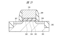
不揮発性メモリセルは、Si基板(半導体基板)上に設けたp型ウェル領域101、素子分離領域102、ソース領域109となるn型拡散層(n型半導体領域)、ドレイン領域110となるn型拡散層(n型半導体領域)を有する2つの電界効果トランジスタから構成されている。なお、本実施の形態1におけるソース領域、ドレイン領域の名称は、読み出し動作時の電圧関係を示しており、逆の名称でも問題はない。
The nonvolatile memory cell includes a p-
選択トランジスタは、ゲート絶縁膜103となるSi酸化膜、コントロールゲート電極(第1導電体)104となるn型多結晶Si膜から構成されている。メモリトランジスタのメモリゲート電極108は、選択トランジスタのコントロールゲート電極104の左側側壁部に自己整合的に形成されている。一方、コントロールゲート電極104の右側側壁部には、サイドウォール111が形成されている。本実施の形態1では、例えば選択トランジスタのゲート長は約150nm、メモリトランジスタのゲート長は約55nmとしている。
The selection transistor is composed of a Si oxide film to be the
メモリトランジスタはp型ウェル領域101との下層電位障壁膜(第1の電位障壁膜)となるボトムSi酸化膜105、電荷保持膜106、上層電位障壁膜(第2の電位障壁膜)となるトップSi酸化膜107およびn型多結晶Si膜から構成されているメモリゲート電極(第2導電体)108よりなる。上述したボトムSi酸化膜105、電荷保持膜106、トップSi酸化膜107がメモリトランジスタの容量絶縁膜であり、かつコントロールゲート電極104とメモリゲート電極108を電気的に分離する側壁絶縁膜も兼ねている。
The memory transistor includes a bottom
選択トランジスタおよびメモリトランジスタの初期のしきい電圧(Vth)は、チャネルが形成されるp型ウェル101表面領域に不純物注入を行うことで、それぞれ約1V、約0Vになるように調整されている。 The initial threshold voltage (Vth) of the selection transistor and the memory transistor is adjusted to about 1 V and about 0 V, respectively, by performing impurity implantation in the surface region of the p-type well 101 where the channel is formed.
選択トランジスタのゲート絶縁膜103およびメモリトランジスタのボトムSi酸化膜105は、例えば、p型ウェル領域101を酸化性雰囲気中で熱酸化して形成したSi酸化膜であり、例えば膜厚はそれぞれ3nmおよび4nmである。本実施の形態1では、選択トランジスタのゲート絶縁膜103やメモリトランジスタのボトムSi酸化膜105として熱酸化を用いた例を示しているが、熱酸化膜を一酸化窒素(NO)や亜酸化窒素(N2O)雰囲気等の窒化性雰囲気中で処理(窒化処理)したSi酸窒化膜を用いることも可能である。
The
電荷保持膜106であるSi3N4膜(試料A)およびSRN膜(試料B、C)は、例えばモノシラン(SiH4)とアンモニア(NH3)を原料ガスとする減圧化学気相成長(LP-CVD:Low Pressure-Chemical Vapor Deposition)法で形成する堆積膜とすることができる。例えば、形成温度は700℃、全圧は100Pa、膜厚は14nmである。ここでは、電荷保持膜106の形成に枚葉式のCVD装置を用い、ガス流量比(NH3/SiH4)を制御することで組成xを調整している。なお、電荷保持膜106の形成にモノシラン(SiH4)とアンモニア(NH3)を原料とするCVD法を使用しているが、これに限らず、例えばジクロルシラン(SiH2Cl2)とアンモニア(NH3)を原料とするCVD法で形成することもできる。
The Si 3 N 4 film (sample A) and the SRN film (samples B and C), which are the
メモリトランジスタのトップSi酸化膜107は、例えば電荷保持膜106を水蒸気酸化したSi酸化膜であり、例えば膜厚は約6nmである。このトップSi酸化膜107の形成工程で、電荷保持膜106の表面は酸化され、その膜厚は減少して約10nmとなっている。ここでは、トップSi酸化膜107の形成に水蒸気酸化を用いた例を示したが、オゾンを用いた酸化やラジカルを用いた酸化を用いることも可能である。また、原料ガスにジクロルシラン(SiH2Cl2)と亜酸化窒素(N2O)を用いた減圧CVD法により、Si酸化膜を堆積してもよい。但し、トップSi酸化膜107をCVD法で形成する場合は、電荷保持膜106の膜厚減少が発生しないので、電荷保持膜106を予め薄めに設定する必要がある。なお、本実施の形態1で示す素子寸法や薄膜の膜厚の絶対値は一例であり、この数値をもって本発明が限定されるわけではない。
また、本実施の形態1では、電荷保持膜106であるSRN膜の形成方法として、モノシラン(SiH4)とアンモニア(NH3)を原料ガスとする熱CVD法の例を示したが、本実施の形態1は原料ガスの種類で限定されるものではなく、Siの供給源(Si化合物)としてモノシラン(SiH4)、ジシラン(Si2H2)、ジクロルシラン(SiH2Cl2)等の水素Si化合物、四塩化シリコン(SiCl4)や六塩化シリコン等のハロゲンSi化合物を使用することができる。また、窒素の供給源として、アンモニア(NH3)の他にヒドラジン(N2H2)などを用いることも無論可能である。その成膜方法としては、プラズマCVD法や触媒CVD法等の他のCVD法を用いても良い。また、スパッタリング(PVD法)を用いてSRN膜を形成してもよい。例えば、Siをターゲットとし窒化性の雰囲気中でスパッタリングを行い、SRN膜を形成する方法などが使用できる。
The top
In the first embodiment, an example of the thermal CVD method using monosilane (SiH 4 ) and ammonia (NH 3 ) as source gases is shown as a method for forming the SRN film that is the
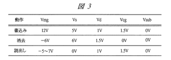
図3に、図1に示す不揮発性メモリセルの動作と電圧の印加電圧の一例を示す。ここでは、電荷保持膜106への電子注入を書込み(Write)、正孔注入を消去(Erase)と定義する。書込みは、選択トランジスタ側からのホットエレクトロン注入であり、消去は、ソース領域端部のバンド間トンネリング(BTBT)により発生したホットホール注入である。
FIG. 3 shows an example of the operation and voltage application voltage of the nonvolatile memory cell shown in FIG. Here, electron injection into the
図3の記号はそれぞれの電極への印加電圧を示しており、Vmgはメモリトランジスタのメモリゲート電極108に印加される電圧を示している。また、Vsはソース領域109に印加される電圧を示しており、Vdはドレイン領域110に印加される電圧を示している。さらに、Vcgは選択トランジスタのコントロールゲート電極104に印加される電圧を示しており、Vsubはp型ウェル領域101に印加される電圧を示している。
The symbol in FIG. 3 indicates the voltage applied to each electrode, and Vmg indicates the voltage applied to the
書込み動作は、例えば、Vmg=12V、Vs=5V、Vd=1V、Vcg=1.5V、Vsub=0Vとし、この電位を例えば、1マイクロ秒間パルスとして印加する。選択トランジスタとメモリトランジスタを電気的に絶縁している極めて狭い領域直下のp型ウェル101表面には、非常に大きな電界がかかる。この電界で加速されたチャネル電子はボトムSi酸化膜105の障壁ポテンシャルよりも大きいエネルギーを持つホットエレクトロンとなり、その一部はメモリゲート電極308の大きい電界により、ボトムSi酸化膜を超えてメモリゲート電極108側に引き込まれ電荷保持膜106に注入される。このようにして、書き込み動作が行なわれる。
In the write operation, for example, Vmg = 12V, Vs = 5V, Vd = 1V, Vcg = 1.5V, Vsub = 0V, and this potential is applied as a pulse for 1 microsecond, for example. A very large electric field is applied to the surface of the p-type well 101 immediately under a very narrow region that electrically isolates the selection transistor and the memory transistor. The channel electrons accelerated by this electric field become hot electrons having energy larger than the barrier potential of the bottom
消去動作は、例えば、Vmg=−6V、Vs=6V、Vd=1.5V、Vcg=0V、Vsub=0Vとし、この電位を例えば、100マイクロ秒間パルスとして印加する。ソース領域109端部では、非常に大きい電界によりバンド間トンネリングが起こり、ボトムSi酸化膜105の障壁ポテンシャルよりも大きいエネルギーを持つホットホールが発生する。ホットホールの一部はメモリゲート電極108の大きい電界により、ボトムSi酸化膜を超えてメモリゲート電極108側へ引き込まれ電荷保持膜106に注入される。このようにして消去動作が行なわれる。
In the erasing operation, for example, Vmg = −6V, Vs = 6V, Vd = 1.5V, Vcg = 0V, Vsub = 0V, and this potential is applied as a pulse, for example, for 100 microseconds. At the end of the
読出し動作は、例えば、Vmg=−5V〜7V、Vs=0V、Vd=1V、Vcg=1.5V、Vsub=0Vとする。すなわち、選択トランジスタをオン状態にし、メモリトランジスタのメモリゲート電極108に、書込み状態のしきい値と消去状態のしきい値との間の電位を印加する。これにより電子を注入したメモリセルはオフ状態を保つが、正孔を注入したメモリセルはオン状態となり、2値の情報を読み出すことができる。
The read operation is, for example, Vmg = −5V to 7V, Vs = 0V, Vd = 1V, Vcg = 1.5V, and Vsub = 0V. That is, the selection transistor is turned on, and a potential between the threshold value in the write state and the threshold value in the erase state is applied to the
なお、図3に示した電圧条件は一例であり、この数値をもって本発明が限定されるわけではない。 Note that the voltage conditions shown in FIG. 3 are merely examples, and the present invention is not limited by these numerical values.
次に、電荷保持膜106が化学量論的なSi3N4膜よりなる試料Aと、電荷保持膜106が化学量論的にSiを過剰に含む試料B、Cについて書込み特性および消去特性を比較した結果を説明する。
Next, the writing characteristics and erasing characteristics of the sample A in which the
図4は書込み特性の比較を行なったグラフであり、図5は消去特性の比較を行なったグラフである。図4において、横軸は書込み時間(sec)を示しており、縦軸はしきい値電圧を示している。図4に示すように、書込み時間が経過するとともに電荷保持膜106に電子が注入されるので、不揮発性メモリのしきい値電圧が上昇していることがわかる。一方、図5において、横軸は消去時間(sec)を示しており、縦軸はしきい値電圧を示している。図5に示すように、消去時間が経過するとともに電荷保持膜106に正孔が注入されるので、不揮発性メモリのしきい値電圧が下降していることがわかる。
FIG. 4 is a graph comparing the write characteristics, and FIG. 5 is a graph comparing the erase characteristics. In FIG. 4, the horizontal axis indicates the write time (sec), and the vertical axis indicates the threshold voltage. As shown in FIG. 4, since electrons are injected into the
両特性の測定は、書換えを行っていない試料に、10回のベリファイ書換えを行ってから実施している。ベリファイ書換えのしきい電圧(Vth)は、書込み側のしきい値電圧を5V(Vth=5V)、消去側のしきい値電圧を−2V(Vth=−2V)としている。つまり、書込み特性は、初期のVth=−2Vからの書込み特性であり、消去特性は、初期のVth=5Vからの消去特性である。以下、書込み側の初期のVth(書き込み深さ)をPV、消去側の初期のVth(消去深さ)をEVと記述する。 The measurement of both characteristics is carried out after 10 verify rewrites are performed on a sample that has not been rewritten. The threshold voltage (Vth) for verify rewriting is set such that the threshold voltage on the write side is 5V (Vth = 5V) and the threshold voltage on the erase side is −2V (Vth = −2V). That is, the write characteristic is the write characteristic from the initial Vth = -2V, and the erase characteristic is the erase characteristic from the initial Vth = 5V. Hereinafter, the initial Vth (writing depth) on the writing side is described as PV, and the initial Vth (erasing depth) on the erasing side is described as EV.
図4に示すように、書込み特性を比較した場合、試料AのSi3N4膜と試料Bの組成x=0.07のSRN膜は、同等の書込み特性を示すが、試料Cの組成x=0.14のSRN膜は、しきい電圧が約4.5V程度から書込み速度の低下が確認される。一方、図5に示すように、消去特性を比較すると、Si3N4膜(試料A)が最も深いレベルまで消去できSRN膜の組成xが大きくなるに伴って消去レベルが低下していることがわかる。これは以下の理由による。 As shown in FIG. 4, when the writing characteristics are compared, the Si 3 N 4 film of sample A and the SRN film of composition B of sample B show equivalent writing characteristics, but the composition x of sample C = 0.14 SRN film, it is confirmed that the writing speed is lowered from the threshold voltage of about 4.5V. On the other hand, as shown in FIG. 5, when comparing the erasing characteristics, the Si 3 N 4 film (sample A) can be erased to the deepest level, and the erasing level decreases as the composition x of the SRN film increases. I understand. This is due to the following reason.
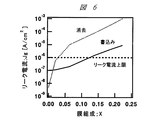
図6はp型Si基板上に作製したMONOSキャパシタのリーク電流と電荷保持膜の組成xとの関係を示す図である。図6において、横軸は電荷保持膜の組成xを示しており、縦軸はリーク電流を示している。キャパシタ絶縁膜(ONO膜)は、ボトムSi酸化膜(4nm)/電荷保持膜(10nm)/トップSi酸化膜(6nm)である。実線は書込み電圧印加時におけるリーク電流密度、破線は消去電圧印加時のリーク電流密度であり、電圧印加後100マイクロ秒経過時のリーク電流を示している。図6から明らかなように、電荷保持膜の組成、すなわちSRN膜の組成xを大きくすると(Si過剰にする)、リーク電流が増加する。特に、消去動作時のリーク電流が大きくなることがわかる。それぞれの膜組成で書込み/消去特性を詳細に調べた結果、ONO膜のリーク電流密度が、約1μA/cm2を境に、書込みレベルの飽和現象や消去レベルが浅くなる現象が観測される。この現象についての原因を、図7を用いて説明する。 FIG. 6 is a diagram showing the relationship between the leakage current of a MONOS capacitor fabricated on a p-type Si substrate and the composition x of the charge retention film. In FIG. 6, the horizontal axis represents the composition x of the charge retention film, and the vertical axis represents the leakage current. The capacitor insulating film (ONO film) is bottom Si oxide film (4 nm) / charge holding film (10 nm) / top Si oxide film (6 nm). The solid line indicates the leak current density when the write voltage is applied, and the broken line indicates the leak current density when the erase voltage is applied, and indicates the leak current when 100 microseconds have elapsed after the voltage application. As is clear from FIG. 6, when the composition of the charge holding film, that is, the composition x of the SRN film is increased (Si is excessive), the leakage current increases. In particular, it can be seen that the leakage current during the erase operation increases. As a result of examining the write / erase characteristics in detail for each film composition, the saturation phenomenon of the write level and the phenomenon that the erase level becomes shallow are observed when the leakage current density of the ONO film is about 1 μA / cm 2 . The cause of this phenomenon will be described with reference to FIG.
図7は消去動作後、一定時間が経過した時のバンドダイアグラムの模式図である。消去開始時は電荷保持膜であるSRN膜内に電子が捕獲されているためメモリゲート電極側からの電子の注入が起こりにくいが(SRN膜領域が上に凸型のバンド構造)、正孔注入で電子が消去されるとトップSi酸化膜にかかる電界は大きくなり、メモリゲート電極側から注入される電子量が増大する。この電子が、Si基板側から注入される正孔と再結合するために、SRN膜に捕獲されている電子が十分に消滅せず、消去時のしきい電圧が浅くなる現象を引き起こす。ここでは、消去時の説明を行ったが、書込み時の現象も同様で、電子を書込んでいると同時に、トップSi酸化膜側に電子がリークすることにより、書込み電圧の飽和現象が発生する。 FIG. 7 is a schematic diagram of a band diagram when a predetermined time has elapsed after the erasing operation. At the start of erasure, electrons are trapped in the SRN film, which is a charge retention film, so that electrons do not easily inject from the memory gate electrode side (the SRN film region has a convex band structure), but hole injection When electrons are erased, the electric field applied to the top Si oxide film increases, and the amount of electrons injected from the memory gate electrode side increases. Since these electrons recombine with holes injected from the Si substrate side, the electrons trapped in the SRN film are not sufficiently eliminated, causing a phenomenon that the threshold voltage during erasure becomes shallow. Although the description at the time of erasing has been made here, the phenomenon at the time of writing is also the same, and at the same time as electrons are written, the electrons leak to the top Si oxide film side, thereby causing a saturation phenomenon of the writing voltage. .
したがって、SRN膜を電荷保持膜として用いる場合は、書込み、消去動作でリーク電流が増大しない範囲で組成を選択することが好ましい。さらに、トップSi酸化膜を少し厚めに設定し、電子のFNリークを抑制することで、SRN膜の使用できる組成範囲を広くすることができる。 Therefore, when the SRN film is used as the charge retention film, it is preferable to select the composition within a range in which the leakage current does not increase in the write and erase operations. Furthermore, the composition range in which the SRN film can be used can be widened by setting the top Si oxide film a little thicker and suppressing FN leakage of electrons.
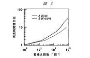
次に、本発明で最も特徴的である書換え耐性に関する説明を行なう。図8は書換え回数に対するサブスレッショルド係数(S値)の変動の比較を示す図であり、図9は消去時間の増加比を示す図である。ここでは、書込み/消去が正常に行える試料A(Si3N4膜)と試料B(SRN膜、x=0.07)の比較を行っている。なお、書換えはPV=5V、EV=−1Vでベリファイ書換えとする。図9の消去時間増加比は、1回目の消去時間とn回目の消去時間との比で示している。両図から明らかなように、SRN膜を用いた試料Bは、Si3N4膜を用いた試料Aに比べ、S値の変動量が小さく、消去時間増加比も小さくなる。これは、Si3N4膜に比べ、SRN膜では書換えに伴う電子と正孔の局在が抑制されていると考えることができる。つまり、不揮発性メモリの電荷保持膜に、化学量論的なSi3N4膜に代えて化学量論的にシリコンを過剰に含むSRN膜を使用することで、電荷保持膜中の電子および正孔の移動度が増加するので、電子および正孔の局在現象を緩和できるのである。電子および正孔の局在現象を緩和できると、電子および正孔の再結合確率を増加させることができ、書換えを多数回行なっても、電荷保持膜中に残存する電荷量を低減できる。したがって、例えば消去動作時、電荷保持膜中に残存する電子の量は少ないので、残存する電子と再結合させる正孔の注入量も減少できる。このため、書換えを多数回行なっても消去時間の増大を抑制することができるのである。また、電荷保持膜中に局在して残存する電荷量を減らすことができるので、S値の劣化も防止できる。 Next, a description will be given of the rewrite endurance characteristic of the present invention. FIG. 8 is a diagram showing a comparison of changes in the subthreshold coefficient (S value) with respect to the number of rewrites, and FIG. Here, a comparison is made between sample A (Si 3 N 4 film) and sample B (SRN film, x = 0.07) that can be normally written / erased. Note that the rewrite is a verify rewrite with PV = 5V and EV = −1V. The erase time increase ratio in FIG. 9 is shown as a ratio between the first erase time and the nth erase time. As is clear from both figures, sample B using the SRN film has a smaller amount of variation in S value and a smaller erase time increase ratio than sample A using the Si 3 N 4 film. This can be considered that localization of electrons and holes associated with rewriting is suppressed in the SRN film as compared with the Si 3 N 4 film. That is, by using an SRN film containing a stoichiometrically excessive amount of silicon instead of the stoichiometric Si 3 N 4 film as the charge holding film of the nonvolatile memory, the electrons and positive charge in the charge holding film can be obtained. Since the hole mobility increases, the localization phenomenon of electrons and holes can be alleviated. If the localization phenomenon of electrons and holes can be alleviated, the recombination probability of electrons and holes can be increased, and the amount of charge remaining in the charge holding film can be reduced even if rewriting is performed many times. Therefore, for example, during the erase operation, the amount of electrons remaining in the charge retention film is small, so that the injection amount of holes recombined with the remaining electrons can also be reduced. For this reason, an increase in the erase time can be suppressed even if rewriting is performed many times. In addition, since the amount of charge remaining localized in the charge holding film can be reduced, the deterioration of the S value can also be prevented.
続いて、データ保持特性に関する説明を行なう。 Next, data retention characteristics will be described.
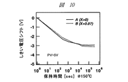
図10と図11にデータ保持特性の比較を示す。図10は書込み側(PV=5V)のデータ保持特性、図11は消去側(EV=−1V)のデータ保持特性で、両者とも初期からの電圧変動量でプロットしている。図10の書込み側のデータ保持特性は無電圧、150℃の結果を、図11の消去側のデータ保持特性は、Vmg=1.5V印加(バイアス加速リテンション)、25℃の結果を示している。 10 and 11 show comparison of data retention characteristics. FIG. 10 shows data holding characteristics on the writing side (PV = 5V), and FIG. 11 shows data holding characteristics on the erasing side (EV = −1V), both of which are plotted with voltage fluctuation amounts from the beginning. The data retention characteristic on the write side in FIG. 10 shows the result at no voltage and 150 ° C., and the data retention characteristic on the erase side in FIG. 11 shows the result at 25 ° C. with Vmg = 1.5 V applied (bias acceleration retention). .
図10に示すように、書込み動作を行なってから時間が経過すると、メモリトランジスタのしきい値電圧が所定値から減少していくが、書込み側の特性は、Si3N4膜とSRN膜に有意差は無い。一方、図11に示すように、消去動作を行なってから時間が経過すると、メモリトランジスタのしきい値電圧が所定値から上昇するが、消去側の特性は、SRN膜の方が良好な特性を示す。消去側のしきい値電圧の上昇は、強反転しているメモリトランジスタのSi基板側から、ボトムSi酸化膜を介して電荷保持膜に電子が流入するために発生する。これは、書換えにより生成されたボトムSi酸化膜中のトラップ準位を介した電子の注入が主原因と考えられる。そこで、SRN膜を用いることで消去に必要な正孔注入量の増加を抑制できる結果、ボトムSi酸化膜の劣化が起こりにくくなる。つまり、SRN膜を用いることで消去に必要な正孔注入量の増加を抑制できるため、正孔がボトムSi酸化膜を通過する際に生じるトラップ準位の生成も低減することができ、電荷保持膜への電子の注入を抑制できる。すなわち、消去側保持特性が改善する。 As shown in FIG. 10, the threshold voltage of the memory transistor decreases from a predetermined value as time elapses after the write operation is performed, but the characteristics on the write side are similar to those of the Si 3 N 4 film and the SRN film. There is no significant difference. On the other hand, as shown in FIG. 11, the threshold voltage of the memory transistor increases from a predetermined value as time elapses after the erase operation is performed, but the characteristics on the erase side are better for the SRN film. Show. The increase in the threshold voltage on the erase side occurs because electrons flow from the Si substrate side of the strongly inverted memory transistor into the charge holding film through the bottom Si oxide film. The main reason for this is considered to be injection of electrons through trap levels in the bottom Si oxide film generated by rewriting. Therefore, by using the SRN film, it is possible to suppress an increase in the amount of hole injection necessary for erasing, so that the bottom Si oxide film is hardly deteriorated. In other words, the use of the SRN film can suppress the increase in the amount of hole injection necessary for erasure, so that the generation of trap levels generated when holes pass through the bottom Si oxide film can be reduced, and charge retention is achieved. Electron injection into the film can be suppressed. That is, the erase side retention characteristics are improved.
以上のように、書込み、消去動作でリーク電流が増大しない範囲で化学量論的にSi組成の大きいSRN膜を電荷保持膜として用いることにより、書換え耐性に優れた両電荷注入型のMONOSメモリを実現することができる。つまり、本実施の形態1によれば、ホットエレクトロンによる電子書込み、ホットホールによる正孔消去を行う不揮発性半導体記憶装置の性能向上を図ることができる。特に、書換えに伴う両電荷注入量の増加を抑制することで書換え耐性を向上させることができる。言い換えれば、サブスレッショルド係数の劣化を抑制することで書換え耐性を向上させることができ、さらにはデータ保持特性の向上を図ることができる。 As described above, by using an SRN film having a stoichiometrically large Si composition as a charge holding film within a range in which a leakage current does not increase in writing and erasing operations, a double charge injection type MONOS memory excellent in rewriting resistance can be obtained. Can be realized. That is, according to the first embodiment, it is possible to improve the performance of a nonvolatile semiconductor memory device that performs electronic writing using hot electrons and hole erasing using hot holes. In particular, the resistance to rewriting can be improved by suppressing an increase in both charge injection amounts associated with rewriting. In other words, the rewrite tolerance can be improved by suppressing the deterioration of the subthreshold coefficient, and further the data retention characteristic can be improved.
次に、本実施の形態1における不揮発性メモリの製造方法について説明する。図12は、本実施の形態1における不揮発性メモリの製造工程を示したフローチャートである。このフローチャートに基づいて製造工程を説明する。 Next, a method for manufacturing the nonvolatile memory according to the first embodiment will be described. FIG. 12 is a flowchart showing a manufacturing process of the nonvolatile memory according to the first embodiment. A manufacturing process is demonstrated based on this flowchart.
まず、Si基板(半導体基板)に素子を分離するための素子分離領域を形成する(S101)。この素子分離領域は、例えば、Si基板に溝を形成し、この溝内を含むSi基板上にSi酸化膜を形成した後、化学的機械的研磨法(CMP:Chemical Mechanical Polishing)法を用いて溝内にだけSi酸化膜を残すSTI(Shallow Trench Isolation)法で形成することができる。 First, an element isolation region for isolating elements is formed on a Si substrate (semiconductor substrate) (S101). The element isolation region is formed by, for example, forming a groove in the Si substrate, forming an Si oxide film on the Si substrate including the inside of the groove, and then using a chemical mechanical polishing (CMP) method. It can be formed by an STI (Shallow Trench Isolation) method that leaves a Si oxide film only in the trench.
続いて、フォトリソグラフィ技術およびイオン注入法を用いて、素子分離領域の間の活性領域にp型ウェルを形成する(S102)。p型ウェルは、例えばホウ素などのp型不純物をSi基板に導入することにより形成される。 Subsequently, a p-type well is formed in the active region between the element isolation regions by using a photolithography technique and an ion implantation method (S102). The p-type well is formed by introducing a p-type impurity such as boron into the Si substrate.
次に、Si基板上にゲート絶縁膜を形成する(S103)。ゲート絶縁膜は、例えば、Si酸化膜からなり、例えば熱酸化法により形成することができる。そして、ゲート絶縁膜上に、例えば多結晶Si膜を堆積した後、フォトリソグラフィ技術およびエッチング技術を使用してパターニングすることにより、多結晶Si膜よりなるコントロールゲート電極を形成する(S104)。 Next, a gate insulating film is formed on the Si substrate (S103). The gate insulating film is made of, for example, a Si oxide film, and can be formed by, for example, a thermal oxidation method. Then, after depositing, for example, a polycrystalline Si film on the gate insulating film, patterning is performed using a photolithography technique and an etching technique, thereby forming a control gate electrode made of the polycrystalline Si film (S104).
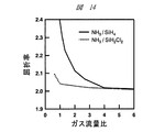
次に、コントロールゲート電極を形成したSi基板上に、ボトムSi酸化膜(第1の電位障壁膜)を形成する(S105)。このボトムSi酸化膜は、例えばSi酸化膜からなり、例えば酸化性雰囲気による熱酸化法を使用して形成することができる。そして、ボトムSi酸化膜上に、電荷保持膜を形成する(S106)。電荷保持膜は、化学量論的にSiを過剰に含むSi窒化膜であるSRN膜から形成される。このSRN膜の形成には、例えば熱CVD法が使用される。この熱CVD法において、原料ガスは、シリコン化合物と窒素化合物が用いられる。具体的に、原料ガスとしてシランとアンモニアあるいはジクロルシランとアンモニアが使用される。この原料ガスは、化学量論的なSi窒化膜であるSi3N4膜を形成する場合と同様であるが、それぞれのガスの流量比を変えることによってSRN膜を形成している。具体的には、後述するが、化学量論的なSi3N4膜を形成する場合は、シランに対するアンモニアの流量比を5以上にして行なわれる。ジクロルシランとアンモニアを使用する場合も同様に、ジクロルシランに対するアンモニアの流量比を5以上にして行なわれる。これに対し、化学量論的にSiを過剰に含むSi窒化膜であるSRN膜を形成する場合、シランに対するアンモニアの流量比を4以下、あるいはジクロルシランに対するアンモニアの流量比を1以下にして行なわれる。ここでのSRN膜は、化学量論的なSi3N4膜を形成する場合の組成ばらつきを超える範囲でSiを過剰に含んでいる。 Next, a bottom Si oxide film (first potential barrier film) is formed on the Si substrate on which the control gate electrode is formed (S105). The bottom Si oxide film is made of, for example, a Si oxide film, and can be formed using, for example, a thermal oxidation method in an oxidizing atmosphere. Then, a charge holding film is formed on the bottom Si oxide film (S106). The charge retention film is formed from an SRN film that is a Si nitride film stoichiometrically containing excessive Si. For example, a thermal CVD method is used to form the SRN film. In this thermal CVD method, a silicon compound and a nitrogen compound are used as the source gas. Specifically, silane and ammonia or dichlorosilane and ammonia are used as source gases. This source gas is the same as in the case of forming a Si 3 N 4 film that is a stoichiometric Si nitride film, but the SRN film is formed by changing the flow rate ratio of each gas. Specifically, as will be described later, when a stoichiometric Si 3 N 4 film is formed, the flow ratio of ammonia to silane is set to 5 or more. Similarly, when dichlorosilane and ammonia are used, the flow rate ratio of ammonia to dichlorosilane is set to 5 or more. On the other hand, when forming an SRN film which is a Si nitride film stoichiometrically containing excessive Si, the flow rate ratio of ammonia to silane is 4 or less, or the flow ratio of ammonia to dichlorosilane is 1 or less. . The SRN film here contains excessive Si in a range that exceeds the composition variation when forming a stoichiometric Si 3 N 4 film.
続いて、電荷保持膜上にトップSi酸化膜(第2の電位障壁膜)を形成する(S107)。このトップSi酸化膜もボトムSi酸化膜と同様に、例えばSi酸化膜から形成され、例えば熱酸化法を用いて形成される。 Subsequently, a top Si oxide film (second potential barrier film) is formed on the charge retention film (S107). Similarly to the bottom Si oxide film, this top Si oxide film is formed of, for example, a Si oxide film, and is formed using, for example, a thermal oxidation method.
その後、トップSi酸化膜上に多結晶Si膜を形成し、フォトリソグラフィ技術およびエッチング技術を使用してパターニングすることにより、メモリゲート電極を形成する(S108)。パターニングでは、多結晶Si膜、トップSi酸化膜、電荷保持膜、およびボトムSi酸化膜が順次加工され、コントロールゲート電極の側壁にだけ、ボトムSi酸化膜、電荷保持膜、トップSi酸化膜および多結晶Si膜を残すことにより、選択トランジスタのコントロール電極の片方の側壁だけに、自己整合的なメモリトランジスタの容量絶縁膜(ONO膜)とメモリゲート電極を形成する。 Thereafter, a polycrystalline Si film is formed on the top Si oxide film, and patterned using a photolithography technique and an etching technique, thereby forming a memory gate electrode (S108). In the patterning, the polycrystalline Si film, the top Si oxide film, the charge holding film, and the bottom Si oxide film are sequentially processed, and the bottom Si oxide film, the charge holding film, the top Si oxide film, and the multi-layer are formed only on the side wall of the control gate electrode. By leaving the crystalline Si film, a self-aligned capacitor insulating film (ONO film) and memory gate electrode of the memory transistor are formed only on one side wall of the control electrode of the selection transistor.
次に、フォトリソグラフィ技術およびエッチング技術を使用して、コントロール電極のもう一方の側壁側をパターニングすることにより、所定のゲート長を有する選択トランジスタを形成する。 Next, a select transistor having a predetermined gate length is formed by patterning the other side wall side of the control electrode by using a photolithography technique and an etching technique.
続いて、フォトリソグラフィ技術およびイオン注入法を使用して側壁にメモリゲート電極を形成したコントロールゲート電極の両側のSi基板内にソース領域およびドレイン領域を形成する(S109)。その後、層間絶縁膜および配線を形成することにより、不揮発性メモリを形成することができる。 Subsequently, a source region and a drain region are formed in the Si substrate on both sides of the control gate electrode in which the memory gate electrode is formed on the side wall using the photolithography technique and the ion implantation method (S109). Thereafter, a nonvolatile memory can be formed by forming an interlayer insulating film and a wiring.
次に、電荷保持膜であるSRN膜を熱CVD法で形成する工程について説明する。図13は、熱CVD装置における処理フローを示すフローチャートである。 Next, a process of forming an SRN film that is a charge holding film by a thermal CVD method will be described. FIG. 13 is a flowchart showing a processing flow in the thermal CVD apparatus.
まず、Si基板(半導体ウェハ)を成膜室にロードした後(S201)、真空パージ(S202)、希ガスパージ(S203)を行いSi基板の温度を安定させる。希ガスパージには下地膜と反応しないガスを用い、一般的には窒素(N2)やアルゴン(Ar)が用いられる。次に希ガスパージを停止した後、Si窒化膜(SRN膜)の原料ガスとなるアンモニアを導入し成膜室を所定の圧力に調整する(S204)。場合によっては、膜厚均一性を確保するためにアンモニアと同時に希ガスも導入する。成膜室の圧力が安定したら、Siを含有する原料ガスを導入し成膜(デポジション)を開始する(S205)。熱CVD法の場合、最も一般的な原料ガスがジクロルシラン(SiH2Cl2)とモノシラン(SiH4)である。所望の膜厚が得られる時間が経過したら、Siを含有する原料ガスだけを停止しアンモニアのポストパージを行う(S206)。この後、アンモニアの導入を停止して真空パージ(S207)、希ガスパージ(S208)を行い、Si基板を成膜室から取り出す(S209)。このようにして電荷保持膜であるSRN膜を形成することができる。 First, after loading a Si substrate (semiconductor wafer) into the film formation chamber (S201), vacuum purge (S202) and rare gas purge (S203) are performed to stabilize the temperature of the Si substrate. For the rare gas purge, a gas that does not react with the base film is used, and nitrogen (N 2 ) or argon (Ar) is generally used. Next, after the rare gas purge is stopped, ammonia as a raw material gas for the Si nitride film (SRN film) is introduced to adjust the film formation chamber to a predetermined pressure (S204). In some cases, in order to ensure film thickness uniformity, a rare gas is also introduced simultaneously with ammonia. When the pressure in the film formation chamber is stabilized, a source gas containing Si is introduced and film formation (deposition) is started (S205). In the case of the thermal CVD method, the most common source gases are dichlorosilane (SiH 2 Cl 2 ) and monosilane (SiH 4 ). When the time for obtaining the desired film thickness has elapsed, only the source gas containing Si is stopped and ammonia post-purge is performed (S206). Thereafter, the introduction of ammonia is stopped, vacuum purge (S207) and rare gas purge (S208) are performed, and the Si substrate is taken out from the film forming chamber (S209). In this manner, an SRN film that is a charge holding film can be formed.
熱CVD法による成膜は、大量のウエハを一括して処理するバッチ方式と、1枚ずつ処理する枚葉方式がある。バッチ方式で成膜する時の原料ガスには、バッチ内の膜厚均一性に優れたジクロルシラン(SiH2Cl2)とアンモニアによる成膜が一般的である。枚葉方式の場合は、シラン(SiH4)とアンモニアによる成膜が主に用いられるが、無論ジクロルシランとアンモニアによる成膜も可能である。
The film formation by the thermal CVD method includes a batch method in which a large number of wafers are processed at once and a single wafer method in which one wafer is processed at a time. As the raw material gas when forming batchwise, film formation with ammonia dichlorosilane having excellent film thickness uniformity in the batch (
上述した熱CVD法によるSi窒化膜の成膜フローは、化学量論的なSi3N4膜を形成する場合と化学量論的にSiを過剰に含むSRN膜を形成する場合でほぼ同様である。以下では、具体的な形態として示した熱CVD法によるSRN膜とSi3N4膜の成膜方法の違いについて記述する。 The flow of forming the Si nitride film by the above-described thermal CVD method is almost the same when forming a stoichiometric Si 3 N 4 film and when forming an SRN film stoichiometrically excessively containing Si. is there. Hereinafter, we describe the differences between SRN film and the Si 3 N 4 film deposition method by thermal CVD method shown as a specific embodiment.
熱CVD法によるSi3N4膜の成膜では、通常Siを含有する原料ガスの導入量よりも窒素を含有する原料ガスの導入量を大きくして成膜する。 In the film formation of the Si 3 N 4 film by the thermal CVD method, the film is generally formed with a larger amount of the source gas containing nitrogen than the amount of the source gas containing Si.
図35は成膜するガス流量比とSi窒化膜の屈折率の関係を示す図である。屈折率は、He−Neレーザー(波長633nm)によるエリプソメトリ法で測定した値である。ガス流量比はNH3流量とSiを含有する原料ガス流量の比を示しており、実線はNH3/SiH4流量比、破線はNH3/SiH2Cl2流量比を示している。シラン(SiH4)を用いた場合は、ガス流量比が約4以下の領域から屈折率が増加し、ジクロルシラン(SiH2Cl2)を用いた場合は、ガス流量比が約1以下の領域から屈折率が増加する。化学量論比の組成を有するSi3N4膜の屈折率は2.0であり、それよりも屈折率が大きくなるSi窒化膜は、化学量論的にSiを過剰に含んだSi窒化膜(SRN膜)であることを示している。 FIG. 35 is a graph showing the relationship between the gas flow rate ratio for film formation and the refractive index of the Si nitride film. The refractive index is a value measured by ellipsometry using a He-Ne laser (wavelength 633 nm). The gas flow rate ratio indicates the ratio of the NH 3 flow rate and the Si-containing source gas flow rate, the solid line indicates the NH 3 / SiH 4 flow rate ratio, and the broken line indicates the NH 3 / SiH 2 Cl 2 flow rate ratio. When silane (SiH 4 ) is used, the refractive index increases from a region where the gas flow rate ratio is about 4 or less, and when dichlorosilane (SiH 2 Cl 2 ) is used, the region where the gas flow rate ratio is about 1 or less. Refractive index increases. The refractive index of the Si 3 N 4 film having the composition of the stoichiometric ratio is 2.0, and the Si nitride film having a refractive index larger than that is the Si nitride film stoichiometrically containing excessive Si. (SRN film).
一般的にSi半導体デバイスに用いられるSi3N4膜は、ガス流量比が多少変化しても屈折率が約2.0より大きくならないガス流量比で成膜する。つまり、図35で示すならば、ガス流量比が5以上の範囲で成膜するのが一般的である。 In general, a Si 3 N 4 film used for a Si semiconductor device is formed at a gas flow rate ratio in which the refractive index does not become larger than about 2.0 even if the gas flow rate ratio changes slightly. That is, as shown in FIG. 35, it is common to form a film with a gas flow ratio of 5 or more.
一方、本実施の形態1では、SRN膜を意図的に形成している。このため、ガス流量比を調節して屈折率が2.0よりも大きくなる範囲で成膜する。具体的には、図35に示すように、シランガスとアンモニアを原料ガスに用いる場合は、シランに対するアンモニアの流量比が4以下になる範囲で成膜する。一方、ジクロルシランとアンモニアを原料ガスに用いる場合は、ジクロルシランに対するアンモニアの流量比が1以下になる範囲で成膜する。このように、Siを含有する原料ガスの割合を高めることで、化学量論的にSiを過剰に含むSRN膜を形成することができる。本実施の形態1で用いるSRN膜とは、屈折率が2.0より大きくなる範囲、言い換えれば、Si3N4膜の組成ばらつきを超える範囲でSiを過剰に含んだSi窒化膜を示している。 On the other hand, in the first embodiment, the SRN film is intentionally formed. Therefore, the film is formed in a range where the refractive index is larger than 2.0 by adjusting the gas flow rate ratio. Specifically, as shown in FIG. 35, when silane gas and ammonia are used as source gas, the film is formed in a range where the flow rate ratio of ammonia to silane is 4 or less. On the other hand, when dichlorosilane and ammonia are used as source gases, the film is formed in a range where the flow ratio of ammonia to dichlorosilane is 1 or less. As described above, by increasing the ratio of the source gas containing Si, an SRN film containing a stoichiometrically excessive amount of Si can be formed. The SRN film used in the first embodiment is a Si nitride film containing excessive Si in a range where the refractive index is larger than 2.0, in other words, in a range exceeding the composition variation of the Si 3 N 4 film. Yes.
(実施の形態2)
図15〜24を用いて本発明の実施の形態2を詳細に説明する。本発明の実施の形態2である不揮発性メモリセルは、前記実施の形態1の図1に示した構造と基本的には同じであり、電荷保持膜106の構成とSRN膜の組成だけが異なっている。
(Embodiment 2)
The second embodiment of the present invention will be described in detail with reference to FIGS. The nonvolatile memory cell according to the second embodiment of the present invention is basically the same as the structure shown in FIG. 1 of the first embodiment except for the configuration of the
図15に本実施の形態2のメモリトランジスタの容量絶縁膜の構成を示す。本実施の形態2では、化学量論的にシリコンを過剰に含むSRN膜106aと化学量論的なSi3N4膜106bの積層構造で電荷保持膜を形成している。SRN膜106aの組成をx=0.2とし、SRN膜106aとSi3N4膜106bとの膜厚比をパラメータとしている。つまり、本実施の形態2で使用するSRN膜の組成はx=0.2であり、前記実施の形態1のx=0.07よりもSiが過剰に含まれている。ここでは膜厚比をRtと記載し、Rt=(tSRN)/(tSi3N4+tSRN)と定義する。なお、SRN膜106aの膜厚とSi3N4膜106bの膜厚を加えた膜厚は10nmで一定としている。
FIG. 15 shows the configuration of the capacitor insulating film of the memory transistor of the second embodiment. In the second embodiment, the charge retention film is formed by a stacked structure of the
図16に本実施の形態2で比較した試料構成を示す。試料AはSi3N4膜の単層膜であり、前記実施の形態1の試料Aに示した試料構成と同じである。試料DはSRN膜とSi3N4膜の積層構造でRt=0.4(SRN膜=4nm、Si3N4膜=6nm)であり、試料EもSRN膜とSi3N4膜の積層構造でRt=0.6(SRN膜=6nm、Si3N4膜=4nm)である。各領域の印加電圧や測定条件は前記実施の形態1と同じである。 FIG. 16 shows a sample configuration compared in the second embodiment. Sample A is a single-layer film of Si 3 N 4 film, and has the same sample configuration as that of sample A of the first embodiment. Sample D has a laminated structure of SRN film and Si 3 N 4 film, and Rt = 0.4 (SRN film = 4 nm, Si 3 N 4 film = 6 nm), and sample E also has a laminated structure of SRN film and Si 3 N 4 film. In the structure, Rt = 0.6 (SRN film = 6 nm, Si 3 N 4 film = 4 nm). The applied voltage and measurement conditions in each region are the same as in the first embodiment.
図17に書込み特性の比較を、図18に消去特性の比較を示す。前記実施の形態1と同様に、書換えを行っていない試料に10回のベリファイ書換えを行った後に測定している。なお、PV=5V、EV=−2Vである。書込み特性は、全ての試料でほぼ同等の結果が得られている。一方、消去特性を比較すると、Rt=0.4の試料Dが単層のSi3N4膜からなる試料Aよりも深いレベルまで消去できていることがわかる。逆に、Rt=0.6の試料Eは単層のSi3N4膜からなる試料Aよりも浅いレベルまでしか消去できていないことがわかる。これも、前記実施の形態1で説明したように消去動作時のONO膜のリーク電流が関与している。すなわち、Rt=0.4の試料Dでは、前記実施の形態1の組成(x=0.07)よりもSiを過剰に含んでいるSRN膜(組成x=0.2)を使用しているので、電子および正孔の局在をより緩和することができ、さらに、SRN膜とSi3N4膜の積層構造としているのでONO膜のリーク電流もあまり問題とならないレベルにすることができる。このため、試料Aよりも深いレベルまで消去できているのである。これに対し、Rt=0.6の試料Eでは、電子および正孔の局在が緩和されているが、リーク電流を抑制するSi3N4膜106bの膜厚に比べてSRN膜106aの膜厚の割合が大きいため、ONO膜のリーク電流が大きくなる。このため、電荷保持膜に正孔を注入する際、メモリゲート電極側から電子が流入してしまうので、試料Aよりも浅いレベルまでしか消去できていないのである。このように、SRN膜106aとSi3N4膜106bとを積層構造にすることで、SRN膜106aの組成xを大きくしながら、リーク電流を低減することができるが、Si3N4膜106bの膜厚に対してSRN膜106aの膜厚を大きくしすぎると、ONO膜のリーク電流が問題となることがわかる。
FIG. 17 shows a comparison of write characteristics, and FIG. 18 shows a comparison of erase characteristics. Similar to the first embodiment, the measurement is performed after verify rewriting is performed 10 times on a sample that has not been rewritten. Note that PV = 5V and EV = −2V. As for the writing characteristics, almost the same results are obtained for all the samples. On the other hand, comparing the erasing characteristics, it can be seen that the sample D with Rt = 0.4 can be erased to a deeper level than the sample A made of the single-layer Si 3 N 4 film. On the contrary, it can be seen that the sample E with Rt = 0.6 can be erased only to a shallower level than the sample A made of the single-layer Si 3 N 4 film. This also involves the leakage current of the ONO film during the erase operation as described in the first embodiment. That is, the sample D with Rt = 0.4 uses an SRN film (composition x = 0.2) containing Si in excess of the composition of the first embodiment (x = 0.07). Therefore, the localization of electrons and holes can be further relaxed, and furthermore, since the SRN film and the Si 3 N 4 film are stacked, the leakage current of the ONO film can be reduced to a level that does not cause much problem. For this reason, it is possible to erase to a deeper level than the sample A. On the other hand, in the sample E with Rt = 0.6, the localization of electrons and holes is relaxed, but the film of the
図19はp型Si基板上に作製したMONOSキャパシタのリーク電流と電荷保持膜の膜厚比Rtの関係を示す図である。キャパシタ絶縁膜(ONO膜)の構成は、ボトムSi酸化膜(4nm)/電荷保持膜(10nm)/トップSi酸化膜(6nm)である。Rt=0はSi3N4単層膜、Rt=1はSRN単層膜に対応する。なおSRN膜の膜組成は、x=0.2で一定である。実線は書込み電圧印加時におけるリーク電流、破線は消去電圧印加時のリーク電流であり、電圧印加後100マイクロ秒経過時のリーク電流を示している。 FIG. 19 is a diagram showing the relationship between the leakage current of the MONOS capacitor fabricated on the p-type Si substrate and the film thickness ratio Rt of the charge retention film. The structure of the capacitor insulating film (ONO film) is bottom Si oxide film (4 nm) / charge holding film (10 nm) / top Si oxide film (6 nm). Rt = 0 corresponds to the Si 3 N 4 single layer film, and Rt = 1 corresponds to the SRN single layer film. The film composition of the SRN film is constant at x = 0.2. A solid line indicates a leak current when a write voltage is applied, and a broken line indicates a leak current when an erase voltage is applied. The leak current when 100 microseconds elapses after the voltage is applied.
図19から明らかなように、電荷保持膜の膜厚比Rtを大きくすると(SRN膜の膜厚比大)リーク電流は増加する。前記実施の形態1で示したように、書込み/消去が遜色なく行えるONO膜のリーク電流はJg=1μA/cm2以下である。書込み条件では3つの試料すべてが書込みを行えるリーク電流であるので、図17に示した書込み特性に差は無い。一方、消去条件では、試料E(Rt=0.6)だけがリーク電流の上限を超えている。このため、試料Eでは浅いレベルまでしか消去できないのである。リーク電流のRt依存性は、トップSi酸化膜側からの電子注入で説明できる。 As is clear from FIG. 19, when the film thickness ratio Rt of the charge retention film is increased (the film thickness ratio of the SRN film is large), the leakage current increases. As shown in the first embodiment, the leakage current of the ONO film that can be written / erased indefinitely is Jg = 1 μA / cm 2 or less. Under the write conditions, all three samples have a leak current that can be written, so there is no difference in the write characteristics shown in FIG. On the other hand, in the erasing condition, only the sample E (Rt = 0.6) exceeds the upper limit of the leakage current. For this reason, the sample E can be erased only to a shallow level. The Rt dependence of the leakage current can be explained by electron injection from the top Si oxide film side.
図20は消去動作後、一定時間が経過した時のバンドダイアグラムの模式図である。本実施の形態2では膜組成x=0.2と非常にリーク電流の大きいSi過剰なSRN膜106aを用いているが、リーク電流の小さいSi3N4膜106bと積層構造にすることで、ONO膜全体のリーク電流を大幅に低減することができている。しかし、図20に示すように、電荷保持膜に保持していた電子がある程度消去されるとトップSi酸化膜とSi3N4膜にかかる電界は大きくなる。これは、抵抗率が小さいSRN膜の膜厚比(Rt)が大きくなるほど顕著になる。このため、Rtを大きくするとメモリゲート電極側から注入される電子量が増大し、消去時の消去レベルが浅くなる。
FIG. 20 is a schematic diagram of a band diagram when a certain time has elapsed after the erasing operation. In the second embodiment, the Si-
したがって、SRN膜を電荷保持膜の一部として用いる場合は、書込み動作と消去動作でリーク電流が増大しない範囲で、SRN膜の組成と膜厚比を選択する必要がある。また、トップSi酸化膜を少し厚めに設定し、電子のFNリークを抑制することで、SRN膜の使用できる組成範囲および膜厚比を広くとることができる。 Therefore, when the SRN film is used as a part of the charge retention film, it is necessary to select the composition and film thickness ratio of the SRN film within a range in which the leakage current does not increase between the write operation and the erase operation. Further, by setting the top Si oxide film a little thicker and suppressing FN leakage of electrons, the usable composition range and film thickness ratio of the SRN film can be widened.
次に、書換え耐性に関する説明を行う。図21に書換え回数に対するサブスレッショルド係数(S値)の変動の比較を、図22に消去時間の増加比を示す。ここでは、書込み/消去が正常に行える試料A(Si3N4単層膜)と試料D(SRN膜/Si3N4膜、Rt=0.4)の比較を行っている。なお、書換えはPV=5V、EV=−1Vでベリファイ書換えとしている。図22の消去時間増加比は、1回目の消去時間とn回目の消去時間との比で示している。両図から明らかなように、SRN/Si3N4積層膜の試料Dは、Si3N4単層膜を用いた試料Aに比べ、S値の変動量も消去時間増加比も小さくなる。これは、SRN膜のSi組成比が大きいため、書換えに伴う電子と正孔の局在が抑制されていることによる。 Next, rewriting tolerance will be described. FIG. 21 shows a comparison of changes in the subthreshold coefficient (S value) with respect to the number of rewrites, and FIG. 22 shows an increase ratio of the erase time. Here, a comparison between sample A (Si 3 N 4 single layer film) and sample D (SRN film / Si 3 N 4 film, Rt = 0.4) that can be normally written / erased is performed. Note that the rewrite is the verify rewrite with PV = 5V and EV = −1V. The erase time increase ratio in FIG. 22 is shown as a ratio between the first erase time and the nth erase time. As is clear from both figures, the sample D of the SRN / Si 3 N 4 laminated film has a smaller S value variation and an erase time increase ratio than the sample A using the Si 3 N 4 single layer film. This is because the SRN film has a large Si composition ratio, so that the localization of electrons and holes accompanying rewriting is suppressed.
図23と図24はデータ保持特性の比較を示す図である。図23は書込み側(PV=5V)のデータ保持特性を示しており、図24は消去側(EV=−1V)のデータ保持特性を示している。両者とも初期からの電圧変動量でプロットしている。図23の書込み側のデータ保持特性は無電圧、150℃の結果を示しており、図24の消去側のデータ保持特性は、Vmg=1.5Vを印加し(バイアス加速リテンション)、25℃の状態で測定した結果を示している。書込み側の特性は、Si3N4単層膜とSRN/Si3N4積層膜に顕著な差は無いが、消去側の特性は、SRN/Si3N4積層膜の方が良好な特性を示す。これは、前記実施の形態1と同様に、SRN/Si3N4積層膜を用いることで消去に必要な正孔注入量の増加を抑制できる結果、ボトムSi酸化膜の劣化が抑制できるためである。 23 and 24 are diagrams showing a comparison of data retention characteristics. FIG. 23 shows the data holding characteristic on the writing side (PV = 5V), and FIG. 24 shows the data holding characteristic on the erasing side (EV = −1V). In both cases, the voltage fluctuation from the beginning is plotted. The data retention characteristic on the writing side in FIG. 23 shows the result of no voltage and 150 ° C., and the data retention characteristic on the erasure side in FIG. 24 applies Vmg = 1.5 V (bias accelerated retention) and 25 ° C. The result measured in the state is shown. There is no significant difference between the Si 3 N 4 single layer film and the SRN / Si 3 N 4 multilayer film on the write side, but the erase side characteristic is better on the SRN / Si 3 N 4 multilayer film. Indicates. This is because, as in the first embodiment, by using the SRN / Si 3 N 4 laminated film, it is possible to suppress an increase in the amount of hole injection necessary for erasing, and as a result, deterioration of the bottom Si oxide film can be suppressed. is there.
以上のように電荷保持膜をSRN膜とSi3N4膜の積層膜にすることにより、リーク電流が増大しないSi組成範囲を、SRN単層膜を用いた場合よりも高くできるので、より電子と正孔の局在を低減して効率的に正孔と電子を再結合させることが可能となる。その結果、書換え耐性に、より優れた両電荷注入型のMONOSメモリを実現できる。 As described above, since the charge retention film is a laminated film of the SRN film and the Si 3 N 4 film, the Si composition range in which the leakage current does not increase can be made higher than that in the case of using the SRN single layer film. It is possible to reduce the localization of holes and to efficiently recombine holes and electrons. As a result, it is possible to realize a double charge injection type MONOS memory that is more excellent in rewriting resistance.
本実施の形態2においては、電荷保持膜の構成としてSRN膜とSi3N4膜との積層構造としているが、現実にはSRN膜106aとSi3N4膜106bの間には薄いSi酸化膜が存在する場合もある。これは、SRN膜106aとSi3N4膜106bを異なる装置で形成する場合であり、大気中の酸素によりSRN膜106aの表面に自然酸化膜が形成されるためである。もし、このようにSRN膜とSi3N4膜の間にSi酸化膜が存在していても、その膜厚が電子や正孔が直接トンネリングを起こす膜厚範囲であれば問題はない。すなわち、膜厚が1.5nm以下であれば本発明と同様の効果が得られる。
In the second embodiment, the charge retention film has a stacked structure of an SRN film and an Si 3 N 4 film, but in reality, a thin Si oxide film is interposed between the
また、本実施の形態2では電荷保持膜の膜構成をSi基板側からSRN膜とSi3N4膜の積層膜として例示したが、電荷保持膜中のSRN膜の配置を換えても問題はない。例えば、Si基板側からSi3N4膜とSRN膜を積層する2層構造や、Si3N4/SRN/Si3N4積層膜、SRN/Si3N4/SRN積層膜などの3層構造でも適用可能である。但し、書込み/消去動作時のONO膜のリーク電流が大きくなり過ぎない範囲で、SRN膜の組成と膜厚比を設定する必要がある。 In the second embodiment, the film structure of the charge holding film is exemplified as a laminated film of the SRN film and the Si 3 N 4 film from the Si substrate side, but there is a problem even if the arrangement of the SRN film in the charge holding film is changed. Absent. For example, a two-layer structure in which a Si 3 N 4 film and an SRN film are stacked from the Si substrate side, or a three- layer structure such as a Si 3 N 4 / SRN / Si 3 N 4 stacked film or an SRN / Si 3 N 4 / SRN stacked film The structure can also be applied. However, it is necessary to set the composition and film thickness ratio of the SRN film within a range in which the leakage current of the ONO film during the write / erase operation does not become too large.
以上、本実施の形態2を例示して書込み特性、消去特性、書換え耐性およびデータ保持特性について記述してきたが、測定条件、測定環境の数値の絶対値は一例であり、この数値をもって本発明が限定されるわけではない。また、本発明においては、図1に示したようにメモリトランジスタが、選択トランジスタの側壁部に自己整合的に形成されている素子構造を例示したが、選択トランジスタのコントロールゲート電極が、メモリトランジスタに乗り上げる構造の素子を用いても、メモリトランジスタのメモリゲート電極が、選択トランジスに乗り上げた逆の素子構造を用いることも可能である。 As described above, the second embodiment has been exemplified to describe the writing characteristics, the erasing characteristics, the rewrite endurance, and the data retention characteristics. However, the absolute values of the numerical values of the measurement conditions and the measurement environment are examples, and the present invention is based on these numerical values. It is not limited. In the present invention, the element structure in which the memory transistor is formed in a self-aligned manner on the side wall portion of the selection transistor as illustrated in FIG. 1 is illustrated, but the control gate electrode of the selection transistor is formed in the memory transistor. It is possible to use the reverse element structure in which the memory gate electrode of the memory transistor rides on the selected transistor even if the element has a structure to ride on.
なお、本実施の形態2における不揮発性メモリの製造方法も前記実施の形態1とほぼ同様である。異なる点は、電荷保持膜をSRN膜とSi3N4膜の積層膜で形成する点である。このように構成されている電荷保持膜を形成するのは、例えば熱CVD法を使用することができる。そして、原料ガスの流量比を調整することにより、SRN膜とSi3N4膜を積層して形成することができる。例えば、原料ガスとしてジクロルシランとアンモニアを用いる場合、ジクロルシランに対するアンモニアの流量比を1以下にすることで、SRN膜を形成し、その後、ジクロルシランに対するアンモニアの流量比を5以上にすることで、Si3N4膜を形成することができる。同様に、原料ガスとしてシランとアンモニアを用いる場合、シランに対するアンモニアの流量比を4以下にすることで、SRN膜を形成し、その後、シランに対するアンモニアの流量比を5以上にすることで、Si3N4膜を形成することができる。 The method for manufacturing the nonvolatile memory in the second embodiment is almost the same as that in the first embodiment. The difference is that the charge retention film is formed of a laminated film of an SRN film and a Si 3 N 4 film. For example, a thermal CVD method can be used to form the charge holding film configured as described above. Then, the SRN film and the Si 3 N 4 film can be stacked by adjusting the flow rate ratio of the source gas. For example, when dichlorosilane and ammonia are used as the source gas, the SRN film is formed by setting the flow rate ratio of ammonia to dichlorosilane to 1 or less, and then the flow rate ratio of ammonia to dichlorosilane is set to 5 or more, so that Si 3 An N 4 film can be formed. Similarly, when silane and ammonia are used as the source gas, an SRN film is formed by setting the flow rate ratio of ammonia to silane to 4 or less, and thereafter, the flow rate ratio of ammonia to silane is set to 5 or more. A 3 N 4 film can be formed.
(実施の形態3)
次に、図25〜27を用いて本発明の実施の形態3を説明する。本発明の実施の形態3である不揮発性メモリセルは、図25に示したようにメモリトランジスタ1つで構成された不揮発性メモリであるが、基本的には前記実施の形態1で示したスプリットゲート型不揮発性メモリセルの、メモリトランジスタ領域とほぼ同じ構造である。実際には図25の上層には配線が存在するが本図でも省略している。
(Embodiment 3)
Next,
不揮発性メモリセル(MONOSメモリセル)は、Si基板(半導体基板)上に設けたp型ウェル領域201、素子分離領域202、ドレイン領域207となるn型拡散層(n型半導体領域)、ソース領域208となるn型拡散層(n型半導体領域)、容量絶縁膜およびゲート電極206となるn型多結晶Si膜を有した1つのMOSトランジスタから構成されている。そして、ゲート電極206の両側の側壁には、サイドウォール209が形成されている。
A non-volatile memory cell (MONOS memory cell) includes a p-
不揮発性メモリセルの書込みは、ソース領域208近傍で発生させるチェネルホットエレクトロンを用い、消去にはソース208端で発生させるホットホールを用いる。両電荷ともに、電荷保持膜204へ注入される。本実施の形態2における不揮発性メモリセルの書込み、消去、読出し条件の一例を図27に示す。
The nonvolatile memory cell is written using channel hot electrons generated near the
容量絶縁膜は、下層電位障壁膜となるボトムSi酸化膜203、電荷保持膜204、上層電位障壁膜となるトップSi酸化膜205から構成されている。ボトムSi酸化膜203およびトップSi酸化膜205の膜厚は、それぞれ、4nm、6nmである。
The capacitor insulating film is composed of a bottom
前記実施の形態1で示したような、選択トランジスタを有するMONOSメモリ(スプリットゲート型)は、非選択セルの読出し電流を選択トランジスタでカットオフできるため、メモリトランジスタのしきい電圧を0V以下まで下げることが可能である。また、読出し速度は、低電圧で動作する高性能の選択トランジスタで制御できるため、高速読み出しが可能という利点がある。 In the MONOS memory (split gate type) having the selection transistor as shown in the first embodiment, since the read current of the non-selected cell can be cut off by the selection transistor, the threshold voltage of the memory transistor is lowered to 0 V or less. It is possible. In addition, since the reading speed can be controlled by a high-performance selection transistor that operates at a low voltage, there is an advantage that high-speed reading is possible.
一方、本実施の形態3で示すような選択トランジスタを具備しないMONOSメモリは、選択セルと非選択セルに同じ読出し電圧が印加されるため、読出しの制約上、しきい電圧(Vth)を小さく設定することができない(約2V)。また、読出しも高電圧が必要なメモリトランジスタの性能で決まるため、スプリットゲート型のような高速読出しは困難である。但し、電子と正孔の空間的な捕獲分布が非常に近いため、スプリットゲート型に比べ両電荷の局在を抑制でき、書換え耐性に優れている利点がある。 On the other hand, in the MONOS memory having no selection transistor as shown in the third embodiment, the same read voltage is applied to the selected cell and the non-selected cell, so that the threshold voltage (Vth) is set to be small due to read restrictions. It cannot be done (about 2V). Further, since reading is also determined by the performance of a memory transistor that requires a high voltage, it is difficult to perform high-speed reading like a split gate type. However, since the spatial trap distribution of electrons and holes is very close, the localization of both charges can be suppressed compared to the split gate type, and there is an advantage of excellent rewrite resistance.
本実施の形態3では、図26に示すように電荷保持膜の組成と膜厚比が異なる3つの試料(A、F、G)を準備する。試料Aは化学量論比のSi3N4単層膜、試料FはSRN単層膜(組成x=0.07)、試料GはSRN/Si3N4積層膜(膜厚比Rt=0.4、組成x=0.2)である。本実施の形態3では、電荷保持膜204以外の膜構成および製造プロセスは全て同じとしている。
In the third embodiment, as shown in FIG. 26, three samples (A, F, G) having different charge retention film compositions and film thickness ratios are prepared. Sample A is a stoichiometric Si 3 N 4 monolayer film, sample F is an SRN monolayer film (composition x = 0.07), and sample G is an SRN / Si 3 N 4 laminated film (film thickness ratio Rt = 0) .4, composition x = 0.2). In the third embodiment, the film configuration and the manufacturing process other than the
本実施の形態3においても、前記実施の形態1と同様に、書込み特性、消去特性、書換え特性および書換え後のデータ保持特性の比較を行っている。その結果、SRN単層膜を用いた試料FおよびSRN/Si3N4積層膜を用いた試料Gは、Si3N4単層膜の試料Aに比べ、消去側のデータ保持特性が大幅に改善している。これにより、書換え回数を飛躍的に向上することができる。 Also in the third embodiment, as in the first embodiment, the write characteristics, erase characteristics, rewrite characteristics, and data retention characteristics after rewriting are compared. As a result, the sample F using the SRN single layer film and the sample G using the SRN / Si 3 N 4 laminated film have significantly larger data retention characteristics on the erasure side than the sample A using the Si 3 N 4 single layer film. It has improved. Thereby, the number of rewrites can be dramatically improved.
以上のように、書込み動作および消去動作においてリーク電流が増大しない範囲でSi組成を大きくしたSRN膜を電荷保持膜として用いることにより、MONOSメモリのセル構造に関わらず、書換え耐性に優れた両電荷注入型のMONOSメモリを実現することができる。すなわち、両電荷書換え型(電子注入による書込み、正孔注入による消去)の不揮発性半導体記憶装置の性能向上を図ることができる。特に、書換えに伴う電荷注入量の増加を抑制することが可能となり、書換え耐性や電荷保持特性の向上を図ることができる。 As described above, by using the SRN film having a large Si composition as a charge holding film in the range where the leakage current does not increase in the writing operation and the erasing operation, both charges excellent in rewriting durability can be obtained regardless of the cell structure of the MONOS memory. An injection type MONOS memory can be realized. In other words, it is possible to improve the performance of a double charge rewritable type (writing by electron injection, erasing by hole injection) nonvolatile semiconductor memory device. In particular, it is possible to suppress an increase in the amount of charge injection associated with rewriting, and it is possible to improve rewriting resistance and charge retention characteristics.
なお、図27に示した電圧条件の絶対値は一例であり、この数値をもって本発明が限定されるわけではない。また、実施の形態1〜3に示すMONOSメモリ構造に限らず、本発明は両電荷注入を用いるMONOSメモリ全般に用いることも無論可能である。 The absolute value of the voltage condition shown in FIG. 27 is an example, and the present invention is not limited by this numerical value. Of course, the present invention is not limited to the MONOS memory structure shown in the first to third embodiments, and can be applied to all MONOS memories using both charge injections.
次に、本実施の形態3における不揮発性メモリの製造方法について説明する。まず、Si基板(半導体基板)に素子を分離するための素子分離領域を形成する。この素子分離領域は、例えば、Si基板に溝を形成し、この溝内を含むSi基板上にSi酸化膜を形成した後、化学的機械的研磨法を用いて溝内にだけSi酸化膜を残すSTI法で形成することができる。 Next, a method for manufacturing the nonvolatile memory according to the third embodiment will be described. First, an element isolation region for isolating elements is formed on a Si substrate (semiconductor substrate). For example, the element isolation region is formed by forming a groove in the Si substrate, forming a Si oxide film on the Si substrate including the inside of the groove, and then forming a Si oxide film only in the groove using a chemical mechanical polishing method. The remaining STI method can be used.
続いて、フォトリソグラフィ技術およびイオン注入法を用いて、素子分離領域の間の活性領域にp型ウェルを形成する。p型ウェルは、例えばホウ素などのp型不純物をSi基板に導入することにより形成される。 Subsequently, a p-type well is formed in the active region between the element isolation regions by using a photolithography technique and an ion implantation method. The p-type well is formed by introducing a p-type impurity such as boron into the Si substrate.
次に、Si基板上に、ボトムSi酸化膜(第1の電位障壁膜)を形成する。このボトムSi酸化膜は、例えばSi酸化膜からなり、例えば熱酸化法を使用して形成することができる。そして、ボトムSi酸化膜上に、電荷保持膜を形成する。電荷保持膜は、化学量論的にSiを過剰に含むSi窒化膜であるSRN膜から形成される。このSRN膜の形成には、例えば熱CVD法が使用される。この熱CVD法において、原料ガスは、シリコン化合物と窒素化合物が用いられる。具体的に、原料ガスとしてシランとアンモニアあるいはジクロルシランとアンモニアが使用される。この原料ガスは、化学量論的なSi窒化膜であるSi3N4膜を形成する場合と同様であるが、それぞれのガスの流量比を変えることによってSRN膜を形成している。化学量論的にSiを過剰に含むSi窒化膜であるSRN膜を形成する場合、シランに対するアンモニアの流量比を4以下、あるいはジクロルシランに対するアンモニアの流量比を1以下にして行なわれる。 Next, a bottom Si oxide film (first potential barrier film) is formed on the Si substrate. The bottom Si oxide film is made of, for example, a Si oxide film, and can be formed using, for example, a thermal oxidation method. Then, a charge holding film is formed on the bottom Si oxide film. The charge retention film is formed from an SRN film that is a Si nitride film stoichiometrically containing excessive Si. For example, a thermal CVD method is used to form the SRN film. In this thermal CVD method, a silicon compound and a nitrogen compound are used as the source gas. Specifically, silane and ammonia or dichlorosilane and ammonia are used as source gases. This source gas is the same as in the case of forming a Si 3 N 4 film that is a stoichiometric Si nitride film, but the SRN film is formed by changing the flow rate ratio of each gas. When forming an SRN film that is a Si nitride film stoichiometrically excessively containing Si, the flow rate ratio of ammonia to silane is 4 or less, or the flow ratio of ammonia to dichlorosilane is 1 or less.
続いて、電荷保持膜上にトップSi酸化膜(第2の電位障壁膜)を形成する。このトップSi酸化膜もボトムSi酸化膜と同様に、例えばSi酸化膜から形成され、例えば熱酸化法を用いて形成される。 Subsequently, a top Si oxide film (second potential barrier film) is formed on the charge retention film. Similarly to the bottom Si oxide film, this top Si oxide film is formed of, for example, a Si oxide film, and is formed using, for example, a thermal oxidation method.
その後、トップSi酸化膜上に多結晶Si膜を形成し、フォトリソグラフィ技術およびエッチング技術を使用してパターニングすることにより、ゲート電極を形成する。パターニングでは、ボトムSi酸化膜、電荷保持膜、トップSi酸化膜および多結晶Si膜が順次加工される。そして、ゲート電極の両側のSi基板内にソース領域およびドレイン領域を形成する。続いて、ゲート電極の側壁にサイドウォールを形成した後、層間絶縁膜および配線を形成することにより、不揮発性メモリを形成することができる。 Thereafter, a polycrystalline Si film is formed on the top Si oxide film, and patterned using a photolithography technique and an etching technique to form a gate electrode. In patterning, a bottom Si oxide film, a charge retention film, a top Si oxide film, and a polycrystalline Si film are sequentially processed. Then, a source region and a drain region are formed in the Si substrate on both sides of the gate electrode. Subsequently, after forming a sidewall on the sidewall of the gate electrode, an interlayer insulating film and a wiring are formed, whereby a nonvolatile memory can be formed.
以上、本発明者によってなされた発明を実施の形態に基づき具体的に説明したが、本発明は前記実施の形態に限定されるものではなく、その要旨を逸脱しない範囲で種々変更可能であることはいうまでもない。 As mentioned above, the invention made by the present inventor has been specifically described based on the embodiment. However, the present invention is not limited to the embodiment, and various modifications can be made without departing from the scope of the invention. Needless to say.
また、本発明の不揮発性メモリは、マイクロコンピュータに用いるなど種々の装置に搭載可能である。 The nonvolatile memory of the present invention can be mounted on various devices such as a microcomputer.
本発明は、不揮発性半導体記憶装置を製造する製造業に幅広く利用することができる。 The present invention can be widely used in the manufacturing industry for manufacturing nonvolatile semiconductor memory devices.
101 p型ウェル領域
102 素子分離領域
103 ゲート絶縁膜
104 コントロールゲート電極
105 ボトムSi酸化膜
106 電荷保持膜
106a SRN膜
106b Si3N4膜
107 トップSi酸化膜
108 メモリゲート電極
109 ソース領域
110 ドレイン領域
111 サイドウォール
201 p型ウェル領域
202 素子分離領域
203 ボトムSi酸化膜
204 電荷保持膜
205 トップSi酸化膜
206 ゲート電極
207 ドレイン領域
208 ソース領域
209 サイドウォール
301 Si基板
302 素子分離領域
303 ゲート絶縁膜
304 コントロールゲート電極
305 Si酸化膜
306 Si窒化膜
307 Si酸化膜
308 メモリゲート電極
309 ソース領域
310 ドレイン領域
101 p-
Claims (18)
(b)前記第1および第2半導体領域間上の前記半導体基板の上部に形成された第1導電体および第2導電体と、
(c)前記第1導電体と前記半導体基板との間に形成された第1絶縁膜と、
(d)前記第2導電体と前記半導体基板との間に形成された第2絶縁膜とを備え、
(e)前記第2絶縁膜は、前記半導体基板上に形成された第1の電位障壁膜と、前記第1の電位障壁膜の上部に形成された電荷保持膜と、前記電荷保持膜の上部に形成された第2の電位障壁膜よりなり、
前記電荷保持膜に電子を注入することで情報の書込みを行い、正孔を注入することで情報の消去を行う不揮発性半導体記憶装置であって、
前記電荷保持膜は、化学量論的にシリコンを過剰に含むSi窒化膜を有することを特徴とする不揮発性半導体記憶装置。 (A) first and second semiconductor regions formed in a semiconductor substrate;
(B) a first conductor and a second conductor formed on the semiconductor substrate between the first and second semiconductor regions;
(C) a first insulating film formed between the first conductor and the semiconductor substrate;
(D) a second insulating film formed between the second conductor and the semiconductor substrate;
(E) The second insulating film includes a first potential barrier film formed on the semiconductor substrate, a charge holding film formed on the first potential barrier film, and an upper part of the charge holding film. A second potential barrier film formed on
A nonvolatile semiconductor memory device that writes information by injecting electrons into the charge retention film and erases information by injecting holes,
The non-volatile semiconductor memory device according to claim 1, wherein the charge retention film includes a Si nitride film that stoichiometrically contains excessive silicon.
(b)前記第1および第2半導体領域間上の前記半導体基板の上部に形成された導電体と、
(c)前記導電体と前記半導体基板との間に形成された絶縁膜とを備え、
(d)前記絶縁膜は、前記半導体基板上に形成された第1の電位障壁膜と、前記第1の電位障壁膜の上部に形成された電荷保持膜と、前記電荷保持膜の上部に形成された第2の電位障壁膜よりなり、
前記電荷保持膜に電子を注入することで情報の書込みを行い、正孔を注入することで情報の消去を行う不揮発性半導体記憶装置であって、
前記電荷保持膜は、化学量論的にSiを過剰に含むSi窒化膜を有することを特徴とする不揮発性半導体記憶装置。 (A) first and second semiconductor regions formed in a semiconductor substrate;
(B) a conductor formed on top of the semiconductor substrate between the first and second semiconductor regions;
(C) comprising an insulating film formed between the conductor and the semiconductor substrate;
(D) The insulating film is formed on a first potential barrier film formed on the semiconductor substrate, a charge holding film formed on the first potential barrier film, and an upper part of the charge holding film. The second potential barrier film formed,
A nonvolatile semiconductor memory device that writes information by injecting electrons into the charge retention film and erases information by injecting holes,
The non-volatile semiconductor memory device, wherein the charge retention film includes a Si nitride film stoichiometrically excessively containing Si.
(a)半導体基板上に第1の電位障壁膜を形成する工程と、
(b)前記第1の電位障壁膜上に電荷保持膜を形成する工程と、
(c)前記電荷保持膜上に第2の電位障壁膜を形成する工程と、
(d)前記第2の電位障壁膜上に導電体膜を形成する工程と、
(e)前記第1の電位障壁膜、前記電荷保持膜、前記第2の電位障壁膜および前記導電体膜をパターニングする工程と、
(f)前記半導体基板中に第1および第2半導体領域を形成する工程とを備え、
前記電荷保持膜は、化学量論的にシリコンを過剰に含むSi窒化膜を有することを特徴とする不揮発性半導体記憶装置の製造方法。 A method for manufacturing a nonvolatile semiconductor memory device, wherein information is written by injecting electrons into a charge retention film that retains charges, and information is erased by injecting holes,
(A) forming a first potential barrier film on the semiconductor substrate;
(B) forming a charge retention film on the first potential barrier film;
(C) forming a second potential barrier film on the charge retention film;
(D) forming a conductor film on the second potential barrier film;
(E) patterning the first potential barrier film, the charge retention film, the second potential barrier film, and the conductor film;
(F) forming first and second semiconductor regions in the semiconductor substrate,
The method of manufacturing a nonvolatile semiconductor memory device, wherein the charge retention film includes a Si nitride film stoichiometrically containing excessive silicon.
Priority Applications (2)
| Application Number | Priority Date | Filing Date | Title |
|---|---|---|---|
| JP2006013276A JP2007194511A (en) | 2006-01-23 | 2006-01-23 | Non-volatile semiconductor memory device and method for manufacturing the same |
| US11/639,134 US8125012B2 (en) | 2006-01-23 | 2006-12-15 | Non-volatile memory device with a silicon nitride charge holding film having an excess of silicon |
Applications Claiming Priority (1)
| Application Number | Priority Date | Filing Date | Title |
|---|---|---|---|
| JP2006013276A JP2007194511A (en) | 2006-01-23 | 2006-01-23 | Non-volatile semiconductor memory device and method for manufacturing the same |
Publications (1)
| Publication Number | Publication Date |
|---|---|
| JP2007194511A true JP2007194511A (en) | 2007-08-02 |
Family
ID=38284690
Family Applications (1)
| Application Number | Title | Priority Date | Filing Date |
|---|---|---|---|
| JP2006013276A Pending JP2007194511A (en) | 2006-01-23 | 2006-01-23 | Non-volatile semiconductor memory device and method for manufacturing the same |
Country Status (2)
| Country | Link |
|---|---|
| US (1) | US8125012B2 (en) |
| JP (1) | JP2007194511A (en) |
Cited By (1)
| Publication number | Priority date | Publication date | Assignee | Title |
|---|---|---|---|---|
| WO2012014992A1 (en) * | 2010-07-30 | 2012-02-02 | 学校法人東海大学 | Non-volatile semiconductor memory device, production method for same, and charge storage film |
Families Citing this family (16)
| Publication number | Priority date | Publication date | Assignee | Title |
|---|---|---|---|---|
| US8320191B2 (en) | 2007-08-30 | 2012-11-27 | Infineon Technologies Ag | Memory cell arrangement, method for controlling a memory cell, memory array and electronic device |
| US7602067B2 (en) * | 2007-12-17 | 2009-10-13 | Spansion Llc | Hetero-structure variable silicon rich nitride for multiple level memory flash memory device |
| JP2009224425A (en) * | 2008-03-14 | 2009-10-01 | Renesas Technology Corp | Manufacturing method of nonvolatile semiconductor storage device and nonvolatile semiconductor storage device |
| CN103066074A (en) * | 2011-10-21 | 2013-04-24 | 华东师范大学 | Double capture-silicon oxide nitride oxide semiconductor (SONOS) memorizer with double layer dielectric charge trapping layer and preparation method thereof |
| US9966477B2 (en) | 2012-12-14 | 2018-05-08 | Cypress Semiconductor Corporation | Charge trapping split gate device and method of fabricating same |
| US9368606B2 (en) | 2012-12-14 | 2016-06-14 | Cypress Semiconductor Corporation | Memory first process flow and device |
| US20140167141A1 (en) | 2012-12-14 | 2014-06-19 | Spansion Llc | Charge Trapping Split Gate Embedded Flash Memory and Associated Methods |
| US8816438B2 (en) | 2012-12-14 | 2014-08-26 | Spansion Llc | Process charging protection for split gate charge trapping flash |
| US8836006B2 (en) | 2012-12-14 | 2014-09-16 | Spansion Llc | Integrated circuits with non-volatile memory and methods for manufacture |
| US20140167220A1 (en) | 2012-12-14 | 2014-06-19 | Spansion Llc | Three dimensional capacitor |
| US10014380B2 (en) | 2012-12-14 | 2018-07-03 | Cypress Semiconductor Corporation | Memory first process flow and device |
| US8822289B2 (en) | 2012-12-14 | 2014-09-02 | Spansion Llc | High voltage gate formation |
| US9209197B2 (en) | 2012-12-14 | 2015-12-08 | Cypress Semiconductor Corporation | Memory gate landing pad made from dummy features |
| US20140167142A1 (en) | 2012-12-14 | 2014-06-19 | Spansion Llc | Use Disposable Gate Cap to Form Transistors, and Split Gate Charge Trapping Memory Cells |
| US20140210012A1 (en) | 2013-01-31 | 2014-07-31 | Spansion Llc | Manufacturing of FET Devices Having Lightly Doped Drain and Source Regions |
| KR20140121614A (en) | 2013-04-08 | 2014-10-16 | 에스케이하이닉스 주식회사 | Nonvolatile memory device |
Citations (6)
| Publication number | Priority date | Publication date | Assignee | Title |
|---|---|---|---|---|
| JPS5834978A (en) * | 1981-08-26 | 1983-03-01 | Matsushita Electronics Corp | Semiconductor memory unit |
| JPS6486562A (en) * | 1987-07-31 | 1989-03-31 | Agency Ind Science Techn | Nonvolatile semiconductor memory |
| JPH05145078A (en) * | 1991-11-22 | 1993-06-11 | Kawasaki Steel Corp | Semiconductor nonvolatile storage element and manufacture thereof |
| JP2004186452A (en) * | 2002-12-04 | 2004-07-02 | Renesas Technology Corp | Nonvolatile semiconductor memory device and its manufacturing method |
| JP2004363513A (en) * | 2003-06-09 | 2004-12-24 | Seiko Epson Corp | Semiconductor memory device and its manufacturing method |
| JP2005039138A (en) * | 2003-07-18 | 2005-02-10 | Nippon Telegr & Teleph Corp <Ntt> | Nonvolatile semiconductor memory device |
Family Cites Families (12)
| Publication number | Priority date | Publication date | Assignee | Title |
|---|---|---|---|---|
| JPH05110114A (en) | 1991-10-17 | 1993-04-30 | Rohm Co Ltd | Nonvolatile semiconductor memory device |
| JPH05343694A (en) | 1992-06-05 | 1993-12-24 | Citizen Watch Co Ltd | Manufacture of nonvolatile semiconductor storage element |
| US5969383A (en) * | 1997-06-16 | 1999-10-19 | Motorola, Inc. | Split-gate memory device and method for accessing the same |
| US6368919B2 (en) * | 1999-01-19 | 2002-04-09 | Micron Technology, Inc. | Method and composite for decreasing charge leakage |
| US6465306B1 (en) * | 2000-11-28 | 2002-10-15 | Advanced Micro Devices, Inc. | Simultaneous formation of charge storage and bitline to wordline isolation |
| US6642573B1 (en) * | 2002-03-13 | 2003-11-04 | Advanced Micro Devices, Inc. | Use of high-K dielectric material in modified ONO structure for semiconductor devices |
| US7012299B2 (en) * | 2003-09-23 | 2006-03-14 | Matrix Semiconductors, Inc. | Storage layer optimization of a nonvolatile memory device |
| JP4546117B2 (en) * | 2004-03-10 | 2010-09-15 | ルネサスエレクトロニクス株式会社 | Nonvolatile semiconductor memory device |
| JP4928773B2 (en) * | 2004-12-10 | 2012-05-09 | 株式会社東芝 | Semiconductor device |
| US7612403B2 (en) * | 2005-05-17 | 2009-11-03 | Micron Technology, Inc. | Low power non-volatile memory and gate stack |
| KR100672829B1 (en) * | 2005-08-31 | 2007-01-22 | 삼성전자주식회사 | Method of manufacturing a charge trapping dielectric and method of manufacturing the sonos non-volatile memory device |
| US7531411B2 (en) * | 2005-10-12 | 2009-05-12 | Macronix International Co., Ltd. | Apparatus and method for a non-volatile memory structure comprising a multi-layer silicon-rich, silicon nitride trapping layer |
-
2006
- 2006-01-23 JP JP2006013276A patent/JP2007194511A/en active Pending
- 2006-12-15 US US11/639,134 patent/US8125012B2/en active Active
Patent Citations (6)
| Publication number | Priority date | Publication date | Assignee | Title |
|---|---|---|---|---|
| JPS5834978A (en) * | 1981-08-26 | 1983-03-01 | Matsushita Electronics Corp | Semiconductor memory unit |
| JPS6486562A (en) * | 1987-07-31 | 1989-03-31 | Agency Ind Science Techn | Nonvolatile semiconductor memory |
| JPH05145078A (en) * | 1991-11-22 | 1993-06-11 | Kawasaki Steel Corp | Semiconductor nonvolatile storage element and manufacture thereof |
| JP2004186452A (en) * | 2002-12-04 | 2004-07-02 | Renesas Technology Corp | Nonvolatile semiconductor memory device and its manufacturing method |
| JP2004363513A (en) * | 2003-06-09 | 2004-12-24 | Seiko Epson Corp | Semiconductor memory device and its manufacturing method |
| JP2005039138A (en) * | 2003-07-18 | 2005-02-10 | Nippon Telegr & Teleph Corp <Ntt> | Nonvolatile semiconductor memory device |
Cited By (2)
| Publication number | Priority date | Publication date | Assignee | Title |
|---|---|---|---|---|
| WO2012014992A1 (en) * | 2010-07-30 | 2012-02-02 | 学校法人東海大学 | Non-volatile semiconductor memory device, production method for same, and charge storage film |
| JPWO2012014992A1 (en) * | 2010-07-30 | 2013-09-12 | 学校法人東海大学 | Nonvolatile semiconductor memory device, manufacturing method thereof, and charge storage film |
Also Published As
| Publication number | Publication date |
|---|---|
| US20070170495A1 (en) | 2007-07-26 |
| US8125012B2 (en) | 2012-02-28 |
Similar Documents
| Publication | Publication Date | Title |
|---|---|---|
| JP2007194511A (en) | Non-volatile semiconductor memory device and method for manufacturing the same | |
| US8343840B2 (en) | Blocking dielectric engineered charge trapping memory cell with high speed erase | |
| KR100890040B1 (en) | Non-volatile memory device having charge trapping layer and method of fabricating the same | |
| CN107408558B (en) | Memory cell with high-k charge trapping layer | |
| US8254175B2 (en) | Semiconductor device and method of manufacturing the same | |
| US10229922B2 (en) | Methods of forming memory devices with isolation structures | |
| US8193577B2 (en) | Nonvolatile semiconductor memory device | |
| JP5336872B2 (en) | Nonvolatile semiconductor memory device and manufacturing method thereof | |
| CN107408498B (en) | Method of forming a semiconductor device having a high-k charge trapping layer | |
| JP2007043147A (en) | Method of forming silicon-rich nanocrystal structure using atomic layer deposition process and method of manufacturing nonvolatile semiconductor device using the same | |
| KR101033221B1 (en) | Non-volatile memory device having charge trapping layer and method of fabricating the same | |
| JP2008277530A (en) | Nonvolatile semiconductor memory device | |
| US20070269972A1 (en) | Method of manufacturing a semiconductor device | |
| US20080093646A1 (en) | Non-volatile memory device and method for fabricating the same | |
| KR100819003B1 (en) | Method for fabricating non-volatile memory device | |
| US20150349143A1 (en) | Semiconductor device and method of manufacturing the same | |
| KR100695820B1 (en) | Non-volatile semiconductor device and method of manufcaturing the same | |
| CN106024889A (en) | Semiconductor device and manufacturing method thereof | |
| JP2002261175A (en) | Nonvolatile semiconductor memory and its manufacturing method | |
| JP2002289708A (en) | Nonvolatile semiconductor memory device and its manufacturing method | |
| TW200924172A (en) | Nonvolatile semiconductor storage device and manufacturing method thereof | |
| JP2006196643A (en) | Nonvolatile semiconductor memory device | |
| KR100695140B1 (en) | Method of Manufacturing for Memory Device comprising Silicon Rich Silicon Oxide Layer | |
| US8723248B2 (en) | Nonvolatile semiconductor storage device | |
| KR100722776B1 (en) | Method of forming a silicon rich nano-crystalline structure using atomic layer deposition process and method of manufacturing a non-volatile semiconductor device using the same |
Legal Events
| Date | Code | Title | Description |
|---|---|---|---|
| A621 | Written request for application examination |
Free format text: JAPANESE INTERMEDIATE CODE: A621 Effective date: 20080624 |
|
| A977 | Report on retrieval |
Free format text: JAPANESE INTERMEDIATE CODE: A971007 Effective date: 20100412 |
|
| A711 | Notification of change in applicant |
Free format text: JAPANESE INTERMEDIATE CODE: A712 Effective date: 20100528 |
|
| A131 | Notification of reasons for refusal |
Free format text: JAPANESE INTERMEDIATE CODE: A131 Effective date: 20111122 |
|
| A02 | Decision of refusal |
Free format text: JAPANESE INTERMEDIATE CODE: A02 Effective date: 20120410 |