JP4546117B2 - Nonvolatile semiconductor memory device - Google Patents
Nonvolatile semiconductor memory device Download PDFInfo
- Publication number
- JP4546117B2 JP4546117B2 JP2004066767A JP2004066767A JP4546117B2 JP 4546117 B2 JP4546117 B2 JP 4546117B2 JP 2004066767 A JP2004066767 A JP 2004066767A JP 2004066767 A JP2004066767 A JP 2004066767A JP 4546117 B2 JP4546117 B2 JP 4546117B2
- Authority
- JP
- Japan
- Prior art keywords
- film
- gate
- side wall
- insulating film
- potential barrier
- Prior art date
- Legal status (The legal status is an assumption and is not a legal conclusion. Google has not performed a legal analysis and makes no representation as to the accuracy of the status listed.)
- Expired - Fee Related
Links
- 239000004065 semiconductor Substances 0.000 title claims description 79
- 239000000758 substrate Substances 0.000 claims description 78
- 238000005036 potential barrier Methods 0.000 claims description 60
- 238000002347 injection Methods 0.000 claims description 18
- 239000007924 injection Substances 0.000 claims description 18
- 230000005641 tunneling Effects 0.000 claims description 4
- XUIMIQQOPSSXEZ-UHFFFAOYSA-N Silicon Chemical compound [Si] XUIMIQQOPSSXEZ-UHFFFAOYSA-N 0.000 claims description 2
- 229910052710 silicon Inorganic materials 0.000 claims description 2
- 239000010703 silicon Substances 0.000 claims description 2
- 229910052581 Si3N4 Inorganic materials 0.000 claims 8
- HQVNEWCFYHHQES-UHFFFAOYSA-N silicon nitride Chemical compound N12[Si]34N5[Si]62N3[Si]51N64 HQVNEWCFYHHQES-UHFFFAOYSA-N 0.000 claims 8
- 239000010408 film Substances 0.000 description 433
- 150000004767 nitrides Chemical class 0.000 description 123
- 238000000034 method Methods 0.000 description 63
- 229910021420 polycrystalline silicon Inorganic materials 0.000 description 39
- 230000003647 oxidation Effects 0.000 description 33
- 238000007254 oxidation reaction Methods 0.000 description 33
- 239000004020 conductor Substances 0.000 description 31
- 239000010410 layer Substances 0.000 description 28
- 238000004519 manufacturing process Methods 0.000 description 24
- LPQOADBMXVRBNX-UHFFFAOYSA-N ac1ldcw0 Chemical compound Cl.C1CN(C)CCN1C1=C(F)C=C2C(=O)C(C(O)=O)=CN3CCSC1=C32 LPQOADBMXVRBNX-UHFFFAOYSA-N 0.000 description 18
- 238000004544 sputter deposition Methods 0.000 description 15
- 230000014759 maintenance of location Effects 0.000 description 14
- 238000009792 diffusion process Methods 0.000 description 11
- 239000007789 gas Substances 0.000 description 11
- 239000002784 hot electron Substances 0.000 description 11
- 238000005268 plasma chemical vapour deposition Methods 0.000 description 9
- OAICVXFJPJFONN-UHFFFAOYSA-N Phosphorus Chemical compound [P] OAICVXFJPJFONN-UHFFFAOYSA-N 0.000 description 8
- 230000015572 biosynthetic process Effects 0.000 description 8
- 238000000151 deposition Methods 0.000 description 8
- 229910052698 phosphorus Inorganic materials 0.000 description 8
- 239000011574 phosphorus Substances 0.000 description 8
- IJGRMHOSHXDMSA-UHFFFAOYSA-N Atomic nitrogen Chemical compound N#N IJGRMHOSHXDMSA-UHFFFAOYSA-N 0.000 description 7
- 230000007423 decrease Effects 0.000 description 7
- 238000001312 dry etching Methods 0.000 description 7
- 230000008569 process Effects 0.000 description 7
- 230000008021 deposition Effects 0.000 description 6
- 230000005684 electric field Effects 0.000 description 6
- 150000002500 ions Chemical class 0.000 description 6
- 238000010586 diagram Methods 0.000 description 5
- 238000004518 low pressure chemical vapour deposition Methods 0.000 description 5
- 238000005546 reactive sputtering Methods 0.000 description 5
- 230000002441 reversible effect Effects 0.000 description 5
- 238000002230 thermal chemical vapour deposition Methods 0.000 description 5
- QGZKDVFQNNGYKY-UHFFFAOYSA-N Ammonia Chemical compound N QGZKDVFQNNGYKY-UHFFFAOYSA-N 0.000 description 4
- KRHYYFGTRYWZRS-UHFFFAOYSA-N Fluorane Chemical compound F KRHYYFGTRYWZRS-UHFFFAOYSA-N 0.000 description 4
- MWUXSHHQAYIFBG-UHFFFAOYSA-N Nitric oxide Chemical compound O=[N] MWUXSHHQAYIFBG-UHFFFAOYSA-N 0.000 description 4
- 230000005284 excitation Effects 0.000 description 4
- 230000006872 improvement Effects 0.000 description 4
- 238000003860 storage Methods 0.000 description 4
- 238000011282 treatment Methods 0.000 description 4
- 238000009279 wet oxidation reaction Methods 0.000 description 4
- 238000005229 chemical vapour deposition Methods 0.000 description 3
- 230000007547 defect Effects 0.000 description 3
- 230000006866 deterioration Effects 0.000 description 3
- 230000000694 effects Effects 0.000 description 3
- 238000002955 isolation Methods 0.000 description 3
- 229910052757 nitrogen Inorganic materials 0.000 description 3
- 238000000059 patterning Methods 0.000 description 3
- 238000004904 shortening Methods 0.000 description 3
- 125000006850 spacer group Chemical group 0.000 description 3
- XKRFYHLGVUSROY-UHFFFAOYSA-N Argon Chemical compound [Ar] XKRFYHLGVUSROY-UHFFFAOYSA-N 0.000 description 2
- GQPLMRYTRLFLPF-UHFFFAOYSA-N Nitrous Oxide Chemical compound [O-][N+]#N GQPLMRYTRLFLPF-UHFFFAOYSA-N 0.000 description 2
- CBENFWSGALASAD-UHFFFAOYSA-N Ozone Chemical compound [O-][O+]=O CBENFWSGALASAD-UHFFFAOYSA-N 0.000 description 2
- BLRPTPMANUNPDV-UHFFFAOYSA-N Silane Chemical compound [SiH4] BLRPTPMANUNPDV-UHFFFAOYSA-N 0.000 description 2
- 229910021529 ammonia Inorganic materials 0.000 description 2
- BUMGIEFFCMBQDG-UHFFFAOYSA-N dichlorosilicon Chemical compound Cl[Si]Cl BUMGIEFFCMBQDG-UHFFFAOYSA-N 0.000 description 2
- 238000005530 etching Methods 0.000 description 2
- 239000012535 impurity Substances 0.000 description 2
- 238000005468 ion implantation Methods 0.000 description 2
- 238000001459 lithography Methods 0.000 description 2
- 230000001590 oxidative effect Effects 0.000 description 2
- 238000002294 plasma sputter deposition Methods 0.000 description 2
- 238000000926 separation method Methods 0.000 description 2
- 239000000126 substance Substances 0.000 description 2
- 239000010409 thin film Substances 0.000 description 2
- 229910007991 Si-N Inorganic materials 0.000 description 1
- 229910006294 Si—N Inorganic materials 0.000 description 1
- 230000002411 adverse Effects 0.000 description 1
- 239000007864 aqueous solution Substances 0.000 description 1
- 229910052786 argon Inorganic materials 0.000 description 1
- QVGXLLKOCUKJST-UHFFFAOYSA-N atomic oxygen Chemical compound [O] QVGXLLKOCUKJST-UHFFFAOYSA-N 0.000 description 1
- 229910001873 dinitrogen Inorganic materials 0.000 description 1
- PZPGRFITIJYNEJ-UHFFFAOYSA-N disilane Chemical compound [SiH3][SiH3] PZPGRFITIJYNEJ-UHFFFAOYSA-N 0.000 description 1
- 238000009826 distribution Methods 0.000 description 1
- 230000009977 dual effect Effects 0.000 description 1
- 230000006870 function Effects 0.000 description 1
- 238000010438 heat treatment Methods 0.000 description 1
- 238000011065 in-situ storage Methods 0.000 description 1
- 238000009413 insulation Methods 0.000 description 1
- 230000010354 integration Effects 0.000 description 1
- 239000011229 interlayer Substances 0.000 description 1
- 238000005259 measurement Methods 0.000 description 1
- 239000012528 membrane Substances 0.000 description 1
- 238000012986 modification Methods 0.000 description 1
- 230000004048 modification Effects 0.000 description 1
- 229910021421 monocrystalline silicon Inorganic materials 0.000 description 1
- 239000001272 nitrous oxide Substances 0.000 description 1
- 239000001301 oxygen Substances 0.000 description 1
- 229910052760 oxygen Inorganic materials 0.000 description 1
- 230000002093 peripheral effect Effects 0.000 description 1
- 239000002994 raw material Substances 0.000 description 1
- 230000003252 repetitive effect Effects 0.000 description 1
- 230000004044 response Effects 0.000 description 1
- 239000000243 solution Substances 0.000 description 1
- 238000003892 spreading Methods 0.000 description 1
- 230000007480 spreading Effects 0.000 description 1
- XLYOFNOQVPJJNP-UHFFFAOYSA-N water Substances O XLYOFNOQVPJJNP-UHFFFAOYSA-N 0.000 description 1
Images


Classifications
-
- H—ELECTRICITY
- H10—SEMICONDUCTOR DEVICES; ELECTRIC SOLID-STATE DEVICES NOT OTHERWISE PROVIDED FOR
- H10B—ELECTRONIC MEMORY DEVICES
- H10B43/00—EEPROM devices comprising charge-trapping gate insulators
- H10B43/30—EEPROM devices comprising charge-trapping gate insulators characterised by the memory core region
-
- H—ELECTRICITY
- H01—ELECTRIC ELEMENTS
- H01L—SEMICONDUCTOR DEVICES NOT COVERED BY CLASS H10
- H01L29/00—Semiconductor devices specially adapted for rectifying, amplifying, oscillating or switching and having potential barriers; Capacitors or resistors having potential barriers, e.g. a PN-junction depletion layer or carrier concentration layer; Details of semiconductor bodies or of electrodes thereof ; Multistep manufacturing processes therefor
- H01L29/40—Electrodes ; Multistep manufacturing processes therefor
- H01L29/401—Multistep manufacturing processes
- H01L29/4011—Multistep manufacturing processes for data storage electrodes
- H01L29/40117—Multistep manufacturing processes for data storage electrodes the electrodes comprising a charge-trapping insulator
-
- H—ELECTRICITY
- H01—ELECTRIC ELEMENTS
- H01L—SEMICONDUCTOR DEVICES NOT COVERED BY CLASS H10
- H01L29/00—Semiconductor devices specially adapted for rectifying, amplifying, oscillating or switching and having potential barriers; Capacitors or resistors having potential barriers, e.g. a PN-junction depletion layer or carrier concentration layer; Details of semiconductor bodies or of electrodes thereof ; Multistep manufacturing processes therefor
- H01L29/66—Types of semiconductor device ; Multistep manufacturing processes therefor
- H01L29/68—Types of semiconductor device ; Multistep manufacturing processes therefor controllable by only the electric current supplied, or only the electric potential applied, to an electrode which does not carry the current to be rectified, amplified or switched
- H01L29/76—Unipolar devices, e.g. field effect transistors
- H01L29/772—Field effect transistors
- H01L29/78—Field effect transistors with field effect produced by an insulated gate
- H01L29/792—Field effect transistors with field effect produced by an insulated gate with charge trapping gate insulator, e.g. MNOS-memory transistors
Landscapes
- Engineering & Computer Science (AREA)
- Microelectronics & Electronic Packaging (AREA)
- Power Engineering (AREA)
- Physics & Mathematics (AREA)
- Ceramic Engineering (AREA)
- Condensed Matter Physics & Semiconductors (AREA)
- General Physics & Mathematics (AREA)
- Computer Hardware Design (AREA)
- Manufacturing & Machinery (AREA)
- Semiconductor Memories (AREA)
- Non-Volatile Memory (AREA)
- Read Only Memory (AREA)
Description
本発明は、不揮発性半導体記憶装置の構造とその製造方法に係り、特に低電圧、高速プログラミングが可能な高信頼性の不揮発性半導体記憶装置及びその製造方法に関する。 The present invention relates to a structure of a nonvolatile semiconductor memory device and a manufacturing method thereof, and more particularly to a highly reliable nonvolatile semiconductor memory device capable of low voltage and high-speed programming and a manufacturing method thereof.
半導体不揮発性メモリセルを論理用半導体装置と同一のシリコン(Si)基板上に混載することで、高機能の半導体装置を実現することが可能になる。それらは、組み込み型マイクロコンピュータとして、産業用機械、家電品、自動車搭載装置などに広く用いられている。 By embedding semiconductor nonvolatile memory cells on the same silicon (Si) substrate as the logic semiconductor device, it is possible to realize a highly functional semiconductor device. These are widely used as embedded microcomputers in industrial machines, household electrical appliances, automobile mounted devices, and the like.
一般的には混載された不揮発性メモリには、そのマイクロコンピュータが必要とするプログラムを格納し、随時、読み出して使用する。このような論理用半導体装置との混載に適した不揮発性メモリのセル構造として、選択用MOS型トランジスタと記憶用MOS型トランジスタからなるスプリットゲート構造のメモリセルが挙げられる。 In general, the embedded nonvolatile memory stores a program required by the microcomputer, and reads and uses it as needed. As a cell structure of a non-volatile memory suitable for mixed mounting with such a logic semiconductor device, there is a split gate memory cell composed of a selection MOS transistor and a storage MOS transistor.
この構造を採用するとメモリを制御する周辺回路の面積が小さくて済むために、混載用途では主流となっている記憶用(メモリ)MOS型トランジスタの電荷保持方式には、電気的に孤立した導電性の多結晶シリコンに電荷を蓄えるフローティングゲート方式と、Si窒化膜のような電荷を蓄積する性質をもつ絶縁膜に電荷を蓄えるMONOS方式がある。 When this structure is used, the area of the peripheral circuit that controls the memory can be reduced. Therefore, the charge retention method of the memory (memory) MOS transistor, which is the mainstream in mixed applications, has electrically isolated conductivity. There are a floating gate method for storing charges in polycrystalline silicon and a MONOS method for storing charges in an insulating film having a property of storing charges such as a Si nitride film.
これら、いずれの電荷保持方式においても、電荷を蓄える領域を絶縁性に優れたSi酸化膜で覆う構成であるが、MONOS方式は絶縁膜に電荷を蓄えるため離散記憶が可能であること、Si酸化膜の欠陥による極端な保持寿命低下がないため信頼性予測が容易なこと、メモリセル構造が単純で論理回路部と混載し易い等の利点がある。更に、Si酸化膜の欠陥による極端な保持寿命低下がないため、Si酸化膜にダメージを与え易いホットホール消去を採用でき、消去時間を飛躍的に短くできることから、近年注目を集めている。なお、ホットホール消去については後で詳述するが、絶縁膜に書き込み情報として蓄えたホットエレクトロンを消去する手段として、メモリセルにホットホールを誘起し、蓄積情報であるエレクトロンを中和して消去する方法である。 In any of these charge retention methods, the charge storage region is covered with a Si oxide film having excellent insulating properties. However, the MONOS method stores charges in the insulation film, so that discrete storage is possible. Since there is no extreme decrease in retention life due to film defects, there are advantages such as easy reliability prediction, simple memory cell structure and easy integration with a logic circuit portion. Furthermore, since there is no extreme decrease in retention life due to defects in the Si oxide film, hot hole erasure that easily damages the Si oxide film can be employed, and the erasure time can be drastically shortened. Although hot hole erasing will be described in detail later, as a means for erasing hot electrons stored as write information in the insulating film, hot holes are induced in the memory cell and the stored information is neutralized and erased. It is a method to do.
特に微細化に適したスプリットゲート構造として、自己整合を利用してメモリMOS型トランジスタをサイドウォールで形成する構造(以下、自己整合スプリットゲート構造という)がある(例えば、特許文献1〜3参照乞う)。
As a split gate structure particularly suitable for miniaturization, there is a structure in which a memory MOS transistor is formed on a sidewall using self-alignment (hereinafter referred to as a self-aligned split gate structure) (see, for example,
この自己整合スプリットゲート構造を採用したMONOSメモリは、メモリMOS型トランジスタのゲート長をリソグラフィーの最小解像寸法以下にできるため、動作電流を大きくできる(動作周波数が増加)、メモリセル面積を大幅に微細化できるなどの利点がある。以下、従来のMONOS型メモリセルの構造と動作を、図15を用いて簡単に説明する。 MONOS memory using this self-aligned split gate structure can reduce the gate length of the memory MOS transistor to less than the minimum resolution dimension of lithography, so that the operating current can be increased (the operating frequency is increased), and the memory cell area is greatly increased. There are advantages such as miniaturization. The structure and operation of a conventional MONOS type memory cell will be briefly described below with reference to FIG.
この不揮発性メモリは、記憶部を構成するメモリMOS型トランジスタQ1と、そのメモリ部を選択して情報を読み出すための選択MOS型トランジスタQ2の、2つのMOS型トランジスタから構成されている。選択MOS型トランジスタQ2の拡散層(ソース領域)406aは共通ソース線に、選択ゲート電極403はワード配線に接続されている。一方、メモリMOS型トランジスタQ1の拡散層(ドレイン領域)406bはビット線に、メモリゲート電極405はメモリゲート配線に接続されている。
The nonvolatile memory includes a memory MOS type transistor Q 1 constituting the storage unit, the selection MOS type transistor Q 2 for reading information by selecting the memory unit, is composed of two MOS transistors. Diffusion layer (source region) 406a of the select MOS transistor Q 2 is the common source line, the
メモリMOS型トランジスタQ1のゲート絶縁膜404は3層膜で構成されており、例えばSi基板401の表面側から、Si酸化膜(第1層膜)404a、Si窒化膜(第2層膜)404bおよびSi酸化膜(第3層膜)404cで構成されている。
The gate insulating film 404 of the memory MOS type transistor Q 1 is consists of a three-layer film, for example, from the surface side of the
ゲート絶縁膜404の膜厚は、第1層膜404aが5〜15nm、第2層膜404bが5〜15nm、第3層膜404cが5〜15nm程度である。
The thickness of the gate insulating film 404 is about 5 to 15 nm for the
メモリMOS型トランジスタQ1のゲート絶縁膜404は、選択MOS型トランジスタQ2のゲート電極403形成後に成膜を行うため、上記選択ゲート電極403の側壁部にも形成される。
The gate insulating film 404 of the memory MOS type transistor Q 1 is, for forming a film after the
第1層膜のSi酸化膜404aの形成には熱酸化法が用いられている。第2層膜のSi窒化膜404bの形成は、段差被覆性に優れた減圧熱CVD法が用いられており、原料ガスにジクロルシラン(SiH2Cl2)とアンモニア(NH3)を用いた方法が一般的である。第3層膜のSi酸化膜404cの形成は、熱酸化法と減圧熱CVD法の2つに大別されるが、一般的には熱酸化法が主流である。
A thermal oxidation method is used to form the first layer
書込み動作は、選択MOS型トランジスタQ2の拡散層(ソース領域)406aおよびそのゲート電極403に所定の電圧を印加して選択MOS型トランジスタQ2をオン状態にすると同時に、メモリMOS型トランジスタQ1の拡散層(ドレイン領域)406bおよびそのゲート電極405に所定の電圧を印加する。例えば、ソース領域406aに0V、選択MOS型トランジスタQ2のゲート電極403に1〜2V、ドレイン領域406bに3〜5V、メモリMOS型トランジスタQ1のゲート電極405に8〜10Vの高電圧を印加する。
Write operation, and at the same time the diffusion layer (source region) 406a and turning on the select MOS transistor Q 2 by applying a predetermined voltage to the
このような電圧条件下では、選択MOS型トランジスタQ2とメモリMOS型トランジスタQ1の境界領域に高電界がかかるため、エネルギーの大きいホットエレクトロンがSi基板401中で発生する。このホットエレクトロンの一部は、高電圧に印加されたメモリゲート電極405側へ注入される。この際、ホットエレクトロンの大部分はメモリMOS型トランジスタQ1のゲート絶縁膜の一部であるSi窒化膜404bに捕獲される。一般には、このような電子注入法をソースサイド・ホットエレクトロン注入、もしくはソースサイドインジェクションと呼んでいる。
In such voltage conditions, because a high electric field is applied to the border region of the select MOS transistor Q 2 and the memory MOS type transistor Q 1, greater hot electron energy occurs in the
消去動作は、メモリMOS型トランジスタQ1のメモリゲート電極405に負バイアス、その拡散層406b(ドレイン領域)に正バイアスを印加し、バンド間トンネリング(BTBT)を用いてホットホールを発生させ、そのホットホールをSi窒化膜404bに注入する方式で行う(ホットホール消去)。例えば、ドレイン領域406bに5〜7V、メモリMOS型トランジスタQ1のゲート電極405に−9〜−11V、ソース領域406aと選択MOS型トランジスタQ2のゲート電極403を0Vもしくはオープン状態として消去を行う。
Erase operation, the memory MOS type transistor to Q 1
読み出し動作は、選択MOS型トランジスタQ2をオン状態にした時、メモリMOS型トランジスタQ1のしきい値電圧の状態により、所定の電流が流れるか否かに応じて記憶情報を読み出す。 Read operation, when the selection MOS type transistor Q 2 in the on state, the state of the threshold voltage of the memory MOS type transistor Q 1, reads the stored information in response to whether or not a predetermined current flows.
図15に示したスプリットゲート構造のMONOSメモリの課題を、図を用いて説明する。図16、図17は、それぞれ図15のA領域を拡大した図である。 The problem of the MONOS memory having the split gate structure shown in FIG. 15 will be described with reference to the drawings. 16 and 17 are enlarged views of the area A in FIG.
上記したように、書込み時にSi基板401中でホットエレクトロンが発生する領域は、選択MOS型トランジスタQ2の選択ゲート電極403とメモリMOS型トランジスタQ1のメモリゲート電極405を電気的に分離している領域近傍の直下である。その位置から発生したホットエレクトロンの一部は、メモリMOS型トランジスタQ1のゲート電界によりゲート電極405エッジ方向へ注入される。この注入されたホットエレクトロンの大部分は捕獲断面積の大きいSi窒化膜404bに捕獲され書込みが行われる。
As described above, the region where hot electrons are generated in the
図16に示したように、上記書込みではホットエレクトロンが、横方向の拡がりを持って矢印方向に注入されるので、その一部が選択MOS型トランジスタQ2のゲート電極403側壁部分、言い換えればL字型になっているSi窒化膜404bの縦方向領域(Si基板に垂直方向)にも注入される。また、捕獲された電子が作るSi窒化膜404b中の内部電界や約150℃の高温環境により、捕獲された電子分布は更に拡がると考えられる。
As shown in FIG. 16, the hot electrons in the writing, since with a lateral extension is injected in the direction of the arrow, a part of the
一方、消去のためのホットホール注入は、図17に示したようにメモリMOS型トランジスタQ1のドレイン406b端から矢印方向に行われる。ドレイン406b端の高電界領域で発生したホットホールは、メモリゲート電極405の電界の影響を受け選択MOS型トランジスタQ2側にわずかに拡がりながらSi窒化膜404bへ注入される。
On the other hand, hot hole injection for erase is performed from the
ホットホールの横方向注入拡がりは注入条件に依存するが、50nm〜80nmと考えられる。図17に示したように、正孔注入領域内に存在する電子はマイクロ秒オーダーで消去されるが、正孔注入領域以外の電子は、正孔密度が非常に小さいため電子の消し残り現象が発生する。電子の消し残り量は、書き換え回数を増す毎に蓄積されるため、最終的には消去を行っても所定のしきい電圧にならない不良を招く。 The lateral injection expansion of hot holes is considered to be 50 to 80 nm, although it depends on the injection conditions. As shown in FIG. 17, electrons existing in the hole injection region are erased on the order of microseconds. However, electrons other than the hole injection region have a very low hole density, so that the phenomenon of unerased electrons remains. appear. Since the remaining erased amount of electrons is accumulated every time the number of rewrites is increased, eventually, even if erasing is performed, a defect that does not become a predetermined threshold voltage is caused.
電子の消し残りを防止するには、メモリMOS型トランジスタQ1のゲート長(Lmg)を更に短くするか、消去時間を非常に長くするかの何れかが必要である。しかし、Lmgを小さくするとパンチスルーが起こるため、Lmgは60nm程度が下限である。 To prevent the unerased electrons, the gate length of the memory MOS type transistor Q 1 (Lmg) further shortening or is required either very long erase time. However, since punch-through occurs when Lmg is reduced, the lower limit of Lmg is about 60 nm.
一方、ホットホール注入時間を長くすると、以下の弊害が顕在化してくる。(1)供給電流を確保するためのチャージポンプ電源回路面積が増大する。(2)ボトムゲート酸化膜404aが劣化し電荷保持時間が減少する。(3)ドレイン406b近傍のSi窒化膜404bに正孔が蓄積し、ホットホール発生効率が低下する。
On the other hand, when the hot hole injection time is lengthened, the following adverse effects become obvious. (1) The area of the charge pump power supply circuit for securing the supply current increases. (2) The bottom
したがって、本発明の目的は、メモリMOS型トランジスタQ1が選択MOS型トランジスタQ2のゲート電極側壁部に自己整合的に形成されたスプリットゲート構造のMONOS不揮発性メモリの特性を向上することにある。特に、消し残り電子を少なくして、書き換え耐性を向上させることにある。また、消去時間を短縮させることで消去電流を低減し、電源回路面積を縮小させることにある。また、消去時間を短縮させることで、ゲート酸化膜404aの劣化を抑制し、電荷保持特性の劣化を防止することにある。
Accordingly, an object of the present invention to improve the characteristics of MONOS non-volatile memory of the split gate structure memory MOS type transistor Q 1 is being self-aligned manner to the gate electrode side wall of the selection MOS type transistor Q 2 . In particular, it is to reduce the number of unerased electrons and improve the rewrite resistance. Another object of the present invention is to reduce the erase current by shortening the erase time and to reduce the power supply circuit area. In addition, by shortening the erasing time, deterioration of the
上記目的を達成することのできる本発明の不揮発性半導体記憶装置の概要を図面により説明する。図18、図19及び図20は、本発明を代表する3つの不揮発性半導体記憶装置の要部断面構成例を模式的に示したものである。 An outline of a nonvolatile semiconductor memory device of the present invention capable of achieving the above object will be described with reference to the drawings. 18, 19 and 20 schematically show a cross-sectional configuration example of a main part of three nonvolatile semiconductor memory devices that represent the present invention.
まず、図18を用いて第1の構造例について説明する。
すなわち、本発明の第1の構造例による不揮発性半導体記憶装置の特徴は、
(a)半導体基板501中に形成された第1半導体領域(ソース)506aおよび第2半導体領域(ドレイン)506bと、
(b)前記第1半導体領域506aおよび第2半導体領域506b間上の前記半導体基板501の上部に形成された第1導電体(選択ゲートSG)503および第2導電体(メモリゲートMG)505と、
(c)前記第1導電体503と前記半導体基板501との間に形成された第1絶縁膜502と、
(d)前記第2導電体505と前記半導体基板501との間に形成された3層の第2絶縁膜(Si酸化膜504a/Si窒化膜504b/Si酸化膜504c)504と、
(e)前記第1導電体503と前記第2導電体との間に形成された2層の第2絶縁膜(Si酸化膜504a/Si酸化膜504c)504を有し、
(f)前記第2導電体505と前記半導体基板501との間に形成された3層の第2絶縁膜504は、前記半導体基板501上の電位障壁膜(Si酸化膜)504aと、その上部のSi窒化膜504bと、その上部の電位障壁膜(Si酸化膜)504cよりなり、
(g)前記第1導電体(SG)503と前記第2導電体(MG)505との間に形成された2層の第2絶縁膜504は、電位障壁膜(Si酸化膜)504aと、その上部の電位障壁膜(Si酸化膜)504cとからなる構造としたことである。
First, a first structure example will be described with reference to FIG.
That is, the characteristics of the nonvolatile semiconductor memory device according to the first structural example of the present invention are as follows:
(A) a first semiconductor region (source) 506a and a second semiconductor region (drain) 506b formed in the
(B) a first conductor (selection gate SG) 503 and a second conductor (memory gate MG) 505 formed on the
(C) a first
(D) a three-layer second insulating film (
(E) having a two-layer second insulating film (
(F) A three-layer second insulating
(G) A two-layer second insulating
つまり、この発明の特徴は、第1導電体(SG)503と第2導電体(MG)505との間に形成される第2絶縁膜504の構造を、電位障壁膜(Si酸化膜)504a及び504cの2層構造としたことにある。
That is, the present invention is characterized in that the structure of the second
従来であれば、この領域の第2絶縁膜504は、2層の電位障壁膜(Si酸化膜)504a、504cの間に電荷保持膜(Si窒化膜)504bの一部を挟持した3層構造であるが、本発明では上記のように、この領域には電荷保持膜(Si窒化膜)504bを形成せず、電位障壁膜(Si酸化膜)504a及び504cの2層構造としたものである。
Conventionally, the second
次に、図19を用いて第2の構造例について説明する。
すなわち、本発明の第2の構造例による不揮発性半導体記憶装置の特徴は、
(a)半導体基板601中に形成された第1半導体領域(ソース)606aおよび第2半導体領域(ドレイン)606bと、
(b)前記第1半導体領域606aおよび第2半導体領域606b間上の前記半導体基板601の上部に形成された第1導電体(選択ゲートSG)603および第2導電体(メモリゲートMG)605と、
(c)前記第1導電体603と前記半導体基板601との間に形成された第1絶縁膜602と、
(d)前記第2導電体605と前記半導体基板601との間、及び前記第1導電体(SG)603と前記第2導電体(MG)605との間に形成された3層の第2絶縁膜(Si酸化膜604a/Si窒化膜604b及び604'b/Si酸化膜604c)604を有し、
前記第2導電体605と前記半導体基板601との間の前記第2絶縁膜604は、電位障壁膜(Si酸化膜)604aと、その上部のSi窒化膜(電荷保持膜)604bと、その上部の電位障壁膜(Si酸化膜)604cとよりなり、
前記第1導電体(SG)603の側壁部に位置するSi窒化膜604'bのSi基板601に近い側の少なくとも一部が、上記Si窒化膜604bの上部に位置する電位障壁膜(Si酸化膜)604cによって切断されている構造としたことにある。
Next, a second structure example will be described with reference to FIG.
That is, the characteristics of the nonvolatile semiconductor memory device according to the second structural example of the present invention are as follows:
(A) a first semiconductor region (source) 606a and a second semiconductor region (drain) 606b formed in the semiconductor substrate 601;
(B) a first conductor (selection gate SG) 603 and a second conductor (memory gate MG) 605 formed on the semiconductor substrate 601 between the
(C) a first
(D) a three-layer second layer formed between the
The second
At least a part of the
次に、図20を用いて第3の構造例について説明する。
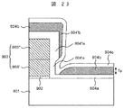
すなわち、本発明の第3の構造例による不揮発性半導体記憶装置の特徴は、
(a)半導体基板701中に形成された第1半導体領域(ソース)706aおよび第2半導体領域(ドレイン)706bと、
(b)前記第1半導体領域706aおよび第2半導体領域706b間上の前記半導体基板701の上部に形成された第1導電体(選択ゲートSG)703および第2導電体(メモリゲートMG)705と、
(c)前記第1導電体703と前記半導体基板701との間に形成された第1絶縁膜702と、
(d)前記第2導電体705と前記半導体基板701との間、及び前記第1導電体(SG)703と前記第2導電体(MG)705との間に形成された3層の第2絶縁膜(Si酸化膜704a/Si窒化膜704b及び704'b/Si酸化膜704c)704を有し、
前記第2導電体705と前記半導体基板701との間の前記第2絶縁膜704は、電位障壁膜(Si酸化膜)704aと、その上部のSi窒化膜(電荷保持膜)704bと、その上部の電位障壁膜(Si酸化膜)704cとからなり、
前記第1導電体(SG)703と前記第2導電体(MG)705との間に位置するSi窒化膜704'bの膜厚が、前記第2導電体705と前記半導体基板701との間に位置するSi窒化膜704の膜厚に比べ薄い構造としたことにある。
Next, a third structure example will be described with reference to FIG.
That is, the feature of the nonvolatile semiconductor memory device according to the third structure example of the present invention is as follows.
(A) a first semiconductor region (source) 706a and a second semiconductor region (drain) 706b formed in the
(B) a first conductor (selection gate SG) 703 and a second conductor (memory gate MG) 705 formed on the
(C) a first
(D) a three-layer second layer formed between the
The second
The film thickness of the
つまり、選択MOS型トランジスタQ2のゲート電極側壁部のSi窒化膜に注入、あるいは拡散した電子は、他の領域の電子に比べ最も電子の消し残りが発生し易い。 That is, the electrons, most electrons unerased tend to occur than that of electrons other areas injected or diffused into the Si nitride film of the gate electrode side wall of the selection MOS type transistor Q 2.
そこで、この第3の構造例では、選択MOS型トランジスタQ2のゲート電極側壁部のSi窒化膜に注入、あるいは拡散する電子量を、他の領域、特に第2導電体(メモリゲートMG)と半導体基板との間の第2絶縁膜の一部を構成するSi窒化膜(電荷保持膜)よりも小さくする点にある。 Therefore, in the third structure example, it injected into the Si nitride film of the gate electrode side wall of the selection MOS type transistor Q 2, or an amount of electron diffusion, and other areas, in particular second conductor (memory gate MG) The point is to make it smaller than the Si nitride film (charge holding film) constituting a part of the second insulating film between the semiconductor substrate.
以上、3つの代表的構造例を基に本発明を概説したが、本発明の要点は、第1の構造例(図18)で説明したように、選択ゲート電極側壁部のSi窒化膜を全て削除する、もしくは第2の構造例(図19)で説明したように、選択ゲート電極側壁部のSi窒化膜の一部分を削除する、もしくは、第3の構造例(図20)で説明したように、選択ゲート電極側壁部のSi窒化膜の膜厚を他の領域(メモリゲートMGと半導体基板との間)の膜厚よりも薄くして消し残り電子の影響を小さくする点にある。 As described above, the present invention has been outlined based on the three typical structural examples. However, as described in the first structural example (FIG. 18), the main point of the present invention is that all of the Si nitride films on the side walls of the select gate electrode. As described in the second structural example (FIG. 19), a part of the Si nitride film on the side wall of the selection gate electrode is deleted, or as described in the third structural example (FIG. 20). The film thickness of the Si nitride film on the side wall of the select gate electrode is made thinner than the film thickness of other regions (between the memory gate MG and the semiconductor substrate) to reduce the influence of unerased electrons.
本発明によれば、ホットホール消去による電子の消し残りが飛躍的に減少し書換え耐性を向上させることができる。 According to the present invention, unerased electrons due to hot hole erasing can be drastically reduced and the rewriting resistance can be improved.
また、本発明によればホットホールによる消去時間が大幅に短縮されるので、消去にかかる消去電流を小さくすることが可能になる。これにより、電源回路の面積が小さくなり製造コストが低減される。 In addition, according to the present invention, the erase time by hot holes is greatly shortened, so that the erase current required for erase can be reduced. This reduces the area of the power supply circuit and reduces the manufacturing cost.
また、本発明によれば、消去時間が大幅に短縮されるので、消去に伴う下層電位障壁膜(ボトムSi酸化膜)の劣化を抑制することができる。これにより電荷保持特性が向上する。 Further, according to the present invention, the erasing time is greatly shortened, so that deterioration of the lower potential barrier film (bottom Si oxide film) accompanying erasing can be suppressed. This improves the charge retention characteristics.
以上の効果を合わせて、本発明によれば、書き換え耐性、及び電荷保持特性に優れた、スプリットゲート構造のMONOS型不揮発メモリを低コストで実現できる。 Combined with the above effects, according to the present invention, it is possible to realize a MONOS type nonvolatile memory having a split gate structure excellent in rewrite endurance and charge retention characteristics at low cost.
以下、本発明の実施例の詳細を、図を用いて説明する。
まず、本発明の中で共通なメモリアレーの構成を図7に示す。各メモリセルは溝型素子分離領域(STI)11で分離されており、ソース線14を共通として、MONOS型不揮発メモリの選択ゲート電極となるワード線12、及びメモリMOS型トランジスタのゲート配線13を平行に配置し、上記ゲート配線12、13を挟んでソース領域14と対称の位置にドレイン15を形成している。図中の16は、ドレイン15とビット線17を接続するための開口部である。ビット線17は、不図示の層間絶縁膜を介してワード線12と直交するように配置されている。
Details of the embodiments of the present invention will be described below with reference to the drawings.
First, FIG. 7 shows a memory array configuration common to the present invention. Each memory cell is separated by a trench type element isolation region (STI) 11, and a
以下、上記図18で説明した第1の構造例を実施例1〜2により、図19で説明した第2の構造例を実施例3により、そして図20で説明した第3の構造例を実施例4により、それぞれ図面にしたがって具体的に説明する。 Hereinafter, the first structural example described in FIG. 18 is performed according to the first and second embodiments, the second structural example illustrated in FIG. 19 is performed according to the third embodiment, and the third structural example illustrated in FIG. 20 is performed. Example 4 will be specifically described with reference to the drawings.
<実施例1>
図1は、本発明の第1の実施例の断面図であり、図7に示したX−Y断面に相当する。図7にはビット線17を示しているが、図1には図示していない。
<Example 1>
FIG. 1 is a cross-sectional view of the first embodiment of the present invention and corresponds to the XY cross section shown in FIG. Although the
本実施例で作製したスプリットゲート構造のMONOS型メモリセルは、Si基板(半導体基板)上に設けたp型ウエル領域(Si基板)101、ソース領域106aとなるn型拡散層(n型半導体領域)、ドレイン領域106bとなるn型拡散層を有した2つのMOS型トランジスタQ1、Q2から構成されている。
The split gate structure MONOS type memory cell fabricated in this example has a p-type well region (Si substrate) 101 provided on a Si substrate (semiconductor substrate) and an n-type diffusion layer (n-type semiconductor region) to be a
選択MOS型トランジスタQ2は、ゲート絶縁膜102となるSi酸化膜、選択ゲート電極(導電体)103となるn型多結晶シリコン膜(以下、「Si膜」という)から構成されている。
The selection MOS transistor Q 2 is composed of a Si oxide film that becomes the
メモリMOS型トランジスタQ1は、p型ウエル領域(Si基板)101との下層電位障壁膜104aとなるSi酸化膜、電荷保持膜104bとなるSi窒化膜、メモリゲート電極105との上層電位障壁膜104cとなるSi酸化膜およびメモリゲート電極105となるn型多結晶Si膜から構成されている。本図に示したように、メモリMOS型トランジスタQ1は、選択MOS型トランシスタQ2に対し自己整合的に形成されている。なお、図1の104'aは、選択MOS型トランシスタQ2の選択ゲート電極側壁部の下層電位障壁膜(Si酸化膜)であり、104'cは、選択ゲート電極側壁部の上層電位障壁膜(Si酸化膜)である。
The memory MOS transistor Q 1 includes a Si oxide film that becomes a lower
次に、本実施例の書込み、消去、読み出し動作の電圧関係を図8に示す。図8に示した印加電圧の各名称は本実施例では共通にしており、選択MOS型トランジスタQ2、及びメモリMOS型トランシスタQ1のゲート電極203、および205に印加する電圧を、それぞれVsg、Vmgで示している。また、ドレイン電圧、ソース電圧は、それぞれVd、Vsで示している。なお、Vwellはウエル電圧であり、本実施例ではSi基板101に印加する電圧となる。なお、図8に示した電圧条件の絶対値は一例であり、この数値をもって本発明が限定されるわけではない。
Next, FIG. 8 shows the voltage relationship of write, erase, and read operations in this embodiment. The names of the applied voltages shown in FIG. 8 are common in this embodiment, and the voltages applied to the selection MOS transistor Q 2 and the
以下、図1〜図6を用いて本実施例の製造方法の詳細を記述する。
まず、図2の断面工程図に示したように、Si基板101上に、周知の技術を用いて不図示の溝形素子分離領域を形成した。この溝型素子分離領域は、図7に示した符合11に相当する。
Hereinafter, the details of the manufacturing method of the present embodiment will be described with reference to FIGS.
First, as shown in the sectional process diagram of FIG. 2, a groove-shaped element isolation region (not shown) was formed on the
次に、選択MOS型トランジスタQ2のゲート絶縁膜102となる3.5nmのSi酸化膜102を熱酸化法で形成した後、窒素ガスで10%に希釈した一酸化窒素(NO)雰囲気中で900℃、10分のNO酸窒化処理を行った。このNO酸窒化処理によれば、Si基板101界面に窒素が約3%程度導入され選択ゲート絶縁膜102としての信頼性が向上する。本実施例では選択ゲート絶縁膜102の信頼性向上のためにNO酸窒化処理を行ったが、一酸化窒素(NO)の代わりに亜酸化窒素(N2O)により酸窒化処理を行ってSi基板101界面に窒素を導入しても同様の効果が得られる。
Next, the
次に、化学気相成長法(CVD法)により、選択ゲート電極103となるリンドープ多結晶Si膜103を200nm堆積した後、周知のリソグラフィー、及びドライエッチング法により所定の電極パターン形状に加工した。なお、上記リンドープ多結晶Si膜103のリン濃度は4e20 atms/cm3とした。続いて、希フッ酸水溶液により上記多結晶Siパターン103以外のゲート絶縁膜102を除去しSi基板101表面を露出させた後、熱酸化法によりSi基板101表面、及びリンドープ多結晶Si膜パターン103表面に熱酸化膜104a、および104'aを形成した。図2に示したように、リンドープ多結晶Si膜パターン103表面の熱酸化膜104'aの膜厚は、単結晶Si基板101表面の熱酸化膜104aの膜厚に比べ厚く形成される。この現象はSi中の不純物(リン)濃度差によるものであるが、この熱酸化膜の膜厚比は、熱酸化雰囲気中の酸素や水分濃度、及び酸化温度で調整することで任意に設定できる。
Next, a phosphorus-doped
本発明では、Si基板101上、及びリンドープ多結晶Siパターン103表面の熱酸化膜の膜厚を、それぞれ5nm、及び13nmに設定した。Si基板101上に形成された5nmの熱酸化膜104aは、図1に示したメモリMOS型トランジスタQ1の下層電位障壁膜104a(以後、ボトムSi酸化膜と略称)となる。なお、上記Si酸化膜104a、及び104'aの個々の膜厚は一例であり、この数値をもって本発明が限定されるわけではない。
In the present invention, the thickness of the thermal oxide film on the
次に、図1に示したメモリMOS型トランジスタの電荷保持膜104bとなるSi窒化膜104bの形成方法を図3により説明する。本発明では、Si窒化膜104bの形成に反応性スパッタ法を適用した。図3には、矢印方向に示したように、リンドープ多結晶Si膜パターン103側壁底部近傍の拡大部分図をも示している。周知のように、Siをターゲットとした平行平板型の反応性スパッタ法によれば、窒素と希ガス(アルゴンガス等)の流量比、電極電力を調整することで高品質のSi窒化膜を堆積することが出来る。
Next, a method of forming the
3図の拡大部分図に示したように、一般に反応性スパッタ法で形成する薄膜は、段差被覆性が非常に悪く、垂直段差側壁部のSi窒化膜104'bの膜厚;Ts、及び段差側壁底部の膜厚;Tcは、段差部から十分離れた平坦部の膜厚;Tpに比べ薄くなる。パターン段差底部のSi窒化膜の膜厚は、パターン段差エッジ部からの距離に依存し、図に示したようにパターン段差エッジ部が最も近い薄い膜厚;Tcとなり、パターン段差エッジから距離;X以上離れた領域でTpとなる。
As shown in the enlarged partial view of FIG. 3, the thin film generally formed by reactive sputtering has very poor step coverage, and the film thickness of the
ここで、段差被覆性RspとRcpを、それぞれRsp=Ts/Tp、Rcp=Tc/Tpと定義すれば、Rsp、Rcp、及びXは、スパッタ条件とパターン段差の高さ(図中のDに対応)に依存する(但し、0<Rsp<1、0<Rcp<1)。 Here, if the step coverage Rsp and Rcp are defined as Rsp = Ts / Tp and Rcp = Tc / Tp, respectively, Rsp, Rcp, and X are the sputtering conditions and the height of the pattern step (D in the figure). (Where 0 <Rsp <1, 0 <Rcp <1).
反応性スパッタ法でSi窒化膜を成膜する場合、例えば、イオンの垂直成分の方向性を重視したロングスロースパッタ法(ターゲットとSi基板の距離を長くしてイオンの方向性を揃える)、コリメーションスパッタ法(コリメータを用いてイオンの方向性を揃える)、2周波励起スパッタ法(Si基板側に低周波電圧を印加してイオンの方向性を揃える)等では、Rsp、Xは小さくなり、Rcpは大きくなる。一方、スパッタ条件が同じであれば、パターン段差;Dが大きいほどRsp、Rcpは小さくなり、Xは大きくなる。すなわち、スパッタ方法、スパッタ条件、パターン段差;Dを調整することで、上記Rsp、Rcp、及びXを任意の大きさにすることができる。 When forming a Si nitride film by the reactive sputtering method, for example, a long throw sputtering method that places importance on the directionality of the vertical component of ions (the distance between the target and the Si substrate is increased to align the directionality of ions), collimation Rsp and X become smaller in the sputtering method (alignment of ion direction using a collimator), two-frequency excitation sputtering method (equalization of ion directionality by applying a low frequency voltage to the Si substrate side), etc. Will grow. On the other hand, if the sputtering conditions are the same, Rsp and Rcp become smaller and X becomes larger as the pattern level difference D increases. That is, by adjusting the sputtering method, sputtering conditions, pattern level difference; D, the Rsp, Rcp, and X can be set to arbitrary sizes.
本実施例では、Si窒化膜104bの形成にアスペクト比の大きいコリメータを用いたコリメーションスパッタ法を適用し、平坦部のSi窒化膜104bの膜厚;Tpが12nmとなるように設定した。この時、リンドープ多結晶Siパターン103側壁エッジ部のSi窒化膜104'bの膜厚;Ts、及びTcは、それぞれ約2.2nm、約6nm、であり、Xは約20nmであった。なお、このTs、Tc、Tp、およびXの絶対値は一例であり、この数値をもって本発明が限定されるわけではない。また、本実施例では、Si窒化膜の形成にコリメーションスパッタ法を用いたが、上述した他のスパッタ法、及び電子サイクロトロン共鳴スパッタ法(ECRスパッタ法)等を用いることも無論可能である。
In this example, collimation sputtering using a collimator with a large aspect ratio was applied to form the
続いて、図4に示したように、950℃のISSG酸化(In-Situ Steam Generation)法を用いて、上記Si窒化膜104bを酸化して、約6nmの上層電位障壁膜(以後、トップSi酸化膜と略称)となるSi酸化膜104cを形成した後、減圧CVD法により、リンを5e20 atms/cm3含んだ厚さ60nmのリンドープ多結晶Si膜105を堆積した。
Subsequently, as shown in FIG. 4, the
上記ISSG酸化法でSi窒化膜104b上に約6nmのトップSi酸化膜を形成した場合、Si窒化膜104は堆積膜厚から約3nm〜3.5nm薄くなる。つまり、トップSi酸化膜を形成する過程で、リンドープ多結晶Siパターン103側壁部の熱酸化膜104'a上のSi窒化膜104'bは全て酸化され、厚さ約4.5nmのSi酸化膜104'cに変換される。すなわち、本発明によれば、電荷保持膜となるSi窒化膜104bは、リンドープ多結晶Siパターン103側壁部には存在しない構造となる。
When a top Si oxide film of about 6 nm is formed on the
本実施例では、トップSi酸化膜104cの形成にISSG酸化法を用いたが、通常のウエット酸化法を適用することも可能である。また、プラズマ酸化やオゾン酸化を用いることも勿論可能である。更に、上記酸化を実施した後、CVD法によりトップSi酸化膜を追加する方法も可能である。但し、ISSG酸化、プラズマ酸化、及びオゾン酸化はラジカル成分による酸化が主体であるため、酸化量を増やしても選択ゲート電極103側壁部分が極端に酸化される形状にはならない。しかし、通常のウエット酸化は水による酸化が主体であるため、酸化量を増やすと選択ゲート電極103側壁部が大幅に酸化される可能性があり、酸化の際には十分注意が必要である。
In this embodiment, the ISSG oxidation method is used to form the top
上述したSi窒化膜104bの酸化に伴う、選択ゲート電極103側壁部の酸化を抑制するには、メモリMOS型トランジスタのボトムSi酸化膜104a形成後にNO酸窒化処理、もしくはN2O酸窒化処理を行う方法が有効である。これらの処理を行えば、ボトムSi酸化膜104aの信頼性を向上できると同時に、選択ゲート電極103側壁部の酸化を抑制できる。無論、Si窒化膜104bの酸化方法にかかわらず酸窒化処理を予め行うことでボトムSi酸化膜の信頼性は向上する。
In order to suppress the oxidation of the side wall portion of the
次に、図5に示したように、異方性ドライエッチングによりリンドープ多結晶Si膜105を選択的にエッチングして、パターン段差側壁部に多結晶Si膜105のサイドスペーサ電極105を形成する。半導体基板上におけるこのサイドスペーサ電極105の幅は、図4で形成した多結晶Si膜105の堆積膜厚で決まり、メモリMOS型トランジスタQ1のゲート長となる。本実施例では、メモリMOS型トランジスタのゲート長を60nmとした。
Next, as shown in FIG. 5, the phosphorus-doped
次に、図5の異方性ドライエッチングにより露出したトップSi酸化膜104c、Si窒化膜104b、及びボトムSi酸化膜104aを順次エッチングして、図6に示したように、選択ゲート電極103となる多結晶Si膜103表面、及びSi基板101表面を露出させた。続いて、所定のレジストパターンを形成して、エッチングにより、もう一方の領域の、リンドープ多結晶Si膜103及びSi酸化膜102のパターンニングを行い、選択MOS型トランジスタQ2のゲート長を規定する。
Next, the top
次に、図1に示したように、イオン注入法でリンを1e15 atms/cm2の密度でSi基板に注入した後、950℃、60秒の熱処理を行いソース106a、ドレイン106bを形成する。
Next, as shown in FIG. 1, phosphorus is implanted into the Si substrate by an ion implantation method at a density of 1e15 atms / cm 2 , followed by heat treatment at 950 ° C. for 60 seconds to form the
この後、選択MOS型トランジスタQ2、及びメモリMOS型トランジスタQ1のゲート電極103及び105側壁部へSi酸化膜のサイドスペーサの形成、上記両電極103及び105表面、ソース領域106a表面、及びドレイン領域106b表面のCoシリサイド化、及びビット線、引き出し配線の形成など一連の周知の工程を経て、図7に示したメモリアレーレイアウトの不揮発性半導体記憶装置を作成し本発明の実施例を完了する。
Thereafter, the side spacers of the Si oxide film are formed on the side walls of the
本実施例で作製したスプリットゲート構造のMONOS不揮発メモリの電気的特性を、図8に示した電圧条件で測定し従来構造と比較した。その結果、読み出し電流、書込み時間は従来メモリと同等の値を示したが、消去時間が約30%短縮した。
これにより、ホットホール消去電流を約30%低減できた。また、繰り返し書込み/消去特性においては電子の消し残りが観測されず、1e5回以上の書き換え耐性が得られた。更に、1e4回の書き込み/消去動作後に150℃の放置リテンション特性(しきい電圧の変動量で定義では)を評価した結果、従来構造に比べ約2桁の改善があった。
The electrical characteristics of the split gate structure MONOS nonvolatile memory fabricated in this example were measured under the voltage conditions shown in FIG. 8 and compared with the conventional structure. As a result, the read current and the write time showed values equivalent to those of the conventional memory, but the erase time was reduced by about 30%.
As a result, the hot hole erase current can be reduced by about 30%. In the repeated write / erase characteristics, no unerased electrons were observed, and a rewrite resistance of 1e5 times or more was obtained. Furthermore, as a result of evaluating the standing retention characteristics at 150 ° C. (defined by the threshold voltage fluctuation amount) after 1e4 write / erase operations, there was an improvement of about two digits compared to the conventional structure.
<実施例2>
次に、図21〜図26を用いて本発明の第2の実施例を説明する。この実施例では、実施例1と同様に、選択ゲート電極側底部に電荷保持膜であるSi窒化膜を形成しない、他の3つの方法について検討した。その結果について以下に順次説明する。
(1)第1の方法について:
図21と図22とを用いて説明する。先ず、図21の断面図に示したように、実施例1と同様にSi基板801上に選択MOS型トランジスタQ2のゲート絶縁膜802を形成した後、ノンドープ多結晶Si膜803を200nm堆積した。
<Example 2>
Next, a second embodiment of the present invention will be described with reference to FIGS. In this example, as in Example 1, other three methods were examined in which a Si nitride film as a charge holding film was not formed on the bottom portion on the side of the select gate electrode. The results will be sequentially described below.
(1) About the first method:
This will be described with reference to FIGS. 21 and 22. First, as shown in the sectional view of FIG. 21, after forming a
次に、選択ゲート電極803となる多結晶Si膜803の表面から約100nmの領域803''に、イオンインプラ法により8e15atms/cm2のリンを注入した。次に、上記多結晶Si膜803を所定の選択ゲート電極の形状にエッチング加工した後、ウエット酸化法によりSi基板801上に5nmのSi酸化膜804aを形成した。このウエット酸化で上記多結晶Si膜803のノンドープ領域803' 表面には膜厚約6nmのSi酸化膜804'aが形成された。一方、リンを高濃度に含んだ領域803''には、不純物が高濃度含まれているため、Si酸化膜804‘aよりも厚い膜厚約20nmのSi酸化膜804''aが形成された。図21は、その断面形状を示している。
Next, phosphorus of 8e15 atoms / cm 2 was implanted into a
続いて、図22の断面図に示すように、2周波励起反応性スパッタ法で、平坦部;Tp膜厚が10nmとなるSi窒化膜804bを堆積した。同スパッタの電極側印加周波数は13.56MHz、基板側周波数は400KHz、基板温度は200℃とした。図22は堆積直後のパターン形状を示す。本実施例においては、多結晶Siパターン803側壁部の形状が、パターン下部に比べパターン上部側壁部のSi酸化膜厚804''aの方が厚くなっているため、Si窒化膜804b堆積前の断面形状はオーバーハング形状となる。
Subsequently, as shown in the cross-sectional view of FIG. 22, a
本実施例で適用した2周波励起スパッタ法は、実施例1で示したコリメーションスパッタ法に比べ段差被覆性が若干向上するため、多結晶Siパターン803側壁部の上部には約3nmのSi窒化膜804'bが形成された。しかし、本実施例においては、多結晶Siパターン803側壁部の形状が、オーバーハング形状となっているため、Si窒化膜804bは側壁段差底部には形成されなかった(図22)。
The dual frequency excitation sputtering method applied in the present embodiment has a slightly improved step coverage as compared with the collimation sputtering method described in the first embodiment. 804'b was formed. However, in this example, since the shape of the side wall portion of the
続いて、トップSi酸化膜804cを形成した。ここでは、図23に示したように、トップSi酸化膜804cを減圧CVD法で形成した場合、及び図24に示したように、ISSG酸化を行った後、減圧CVD法でSi酸化膜を堆積した場合の、2つの試料を作製した。この後、実施例1と同様の製法を用いてスプリットゲート構造のMONOSメモリ(図1参照)を作製した。
(2)第2の方法について:
次に、図25を用いて第2の方法の説明を行う。上記第1の方法と同様に、Si基板901上に選択MOS型トランジスタQ2のゲート酸化膜902を形成した後、リンを5e20 atms/cm3含んだ150nmの多結晶Si膜903を堆積した。
Subsequently, a top
(2) About the second method:
Next, the second method will be described with reference to FIG. As with the first method, after forming a
続いて、減圧CVD法により、厚さ50nmのSi酸化膜907を堆積した後、周知の技術を用いて、上記Si酸化膜907、及び多結晶Si膜903を所定の選択ゲート電極の形状に加工した。多結晶Si膜903をパターンニングした後、等方性ドライエッチング法により上記多結晶Si膜903をSi酸化膜907パターンエッジから後退させた。この多結晶Si膜903の後退量;Zは、ドライエッチング時間により任意に設定できる。本実施例では、後退量;Zを30nmとしたが、Zを大きくしすぎると電荷保持膜となるSi窒化膜904bに電子が注入できなくなるため、後退量Zは40nm以下にすることが好ましい。
Subsequently, after depositing a 50 nm thick
続いて、上記第1の方法と同じ方法でボトムSi酸化膜904a及びSi窒化膜904bを形成した。本方法によれば、選択ゲート電極903上部に形成したSi酸化膜パターン907がオーバーハング形状となるため、図25に示したように、選択ゲート電極903側壁部にはSi窒化膜904が形成されない構造となる。
Subsequently, a bottom
本実施例では、多結晶Si膜903の後退量;Zを30nmとしたが、この絶対値は一例であり、この数値をもって本発明が限定されるわけではない。この後、実施例1と同様の製法を用いてスプリットゲート構造のMONOSメモリ(図1参照)を作製した。
(3)第3の方法について:
次に、図26を用いて第3の方法の説明を行う。上記第1の方法と同様に、Si基板111上に選択MOS型トランジスタQ2のゲート酸化膜112を形成した後、リンを5e20 atms/cm3含んだ150nmの多結晶Si膜113を堆積した。続いて、減圧CVD法により、厚さ50nmのSi酸化膜117を堆積した後、周知の技術を用いて、上記Si酸化膜117を所定の形状に加工し、下地の多結晶Si膜113を露出させた。
In this embodiment, the receding amount of the
(3) About the third method:
Next, the third method will be described with reference to FIG. As with the first method, after forming a gate oxide film 112 of the selection MOS type transistor Q 2 on the
続いて、ドライエッチングの条件を最適化して、多結晶Si膜113を逆テーパ形状に加工した。この多結晶Si膜113の逆テーパ角度;θは、ドライエッチング条件により任意に設定できる。本実施例では、逆テーパ角度;θを80°としたが、逆テーパ角度を小さくすると加工バラツキが増える。従って、上記逆テーパの角度;θは、75°以上90°以下にすることが好ましい。
Subsequently, the conditions for dry etching were optimized, and the
続いて、上記第1の方法と同じ方法でボトムSi酸化膜114a及びSi窒化膜114bを形成した。本方法によれば、選択ゲート電極113をオーバーハング形状にしているため、図26に示したように、選択ゲート電極113側壁部にはSi窒化膜114が形成されない構造となる。この後、実施例1と同様の製法を用いてスプリットゲート構造のMONOSメモリ(図1参照)を作製した。
Subsequently, a bottom
以上、本実施例で示した3つの方法で作製したスプリットゲート構造のMONOS不揮発メモリの電気的特性を、図8に示した電圧条件で測定し従来構造と比較した。その結果、読み出し電流、書込み時間は従来メモリと同等の値を示したが、消去時が約30%短縮した。
これにより、ホットホール消去電流を約30%低減できた。
As described above, the electrical characteristics of the MONOS nonvolatile memory having the split gate structure manufactured by the three methods shown in this example were measured under the voltage condition shown in FIG. 8 and compared with the conventional structure. As a result, the read current and the write time showed values equivalent to those of the conventional memory, but the erase time was reduced by about 30%.
As a result, the hot hole erase current can be reduced by about 30%.
また、繰り返し書込み/消去特性においては電子の消し残りが観測されず、第1の実施例と同様に1e6回以上の書き換え耐性が得られた。更に、1e4回の書き込み/消去動作後に150℃の放置リテンション特性(しきい電圧の変動量で定義では)を評価した結果、従来構造に比べ約2桁の改善があった。 Further, in the repeated write / erase characteristics, no unerased electrons were observed, and a rewrite resistance of 1e6 times or more was obtained as in the first embodiment. Furthermore, as a result of evaluating the retention retention characteristic at 150 ° C. (defined by the amount of variation in the threshold voltage) after 1e4 write / erase operations, there was an improvement of about two digits compared to the conventional structure.
<実施例3>
次に、本発明の第3の実施例を説明する。この実施例は先に図19で概説した第2の構造例に該当するものであり、図9〜図13の断面工程図にしたがって説明する。本実施例でも、メモリアレーの構成(図7参照)、及び各電圧の設定(図8参照)は実施例1と同様である。
<Example 3>
Next, a third embodiment of the present invention will be described. This embodiment corresponds to the second structural example outlined above with reference to FIG. 19, and will be described with reference to the sectional process diagrams of FIGS. Also in this embodiment, the configuration of the memory array (see FIG. 7) and the setting of each voltage (see FIG. 8) are the same as those in the first embodiment.
図9に示したように、まず、実施例1と同様の方法で、p型ウエル領域201(Si基板)上に選択MOS型トランジスタQ2のゲート絶縁膜202の形成、選択ゲート電極203となるリンドープ多結晶Si膜203のパターン形成、及びメモリMOS型トランジスタQ1のボトムSi酸化膜204aを形成した。続いて、電荷保持膜となるSi窒化膜204bをプラズマCVD法で形成した。
As shown in FIG. 9, first, in the same manner as in Example 1, the formation of the p-type well region 201 (Si substrate)
周知のように、SiH2Cl2とNH3を原料ガスとする熱CVD法で形成するSi窒化膜は、ほぼ100%の段差被覆性を示すが、プラズマCVD法は熱CVD法に比べ大幅に段差被覆性が劣化する。例えば、SiH4(モノシラン)とNH3、及びN2を原料ガスとするプラズマCVD法で形成したSi窒化膜は、図9に示したように、パターンの上部段差部でオーバーハング形状になり、段差側壁部204'bの膜厚は、段差の上部から底面に向かって堆積膜厚が減少する。
As is well known, the Si nitride film formed by the thermal CVD method using SiH 2 Cl 2 and NH 3 as source gases shows almost 100% step coverage, but the plasma CVD method is significantly more than the thermal CVD method. The step coverage is deteriorated. For example, a Si nitride film formed by a plasma CVD method using SiH 4 (monosilane), NH 3 , and N 2 as source gases has an overhang shape at the upper step portion of the pattern, as shown in FIG. As for the film thickness of the step
特に、パターン側壁底部(パターン下部のエッジ領域、矢印でシームと表示)は、堆積条件によっては平坦部の膜厚にくらべ約40%程度の膜厚まで減少する。本実施例で示すプラズマCVDで形成したSi窒化膜の堆積形状は、実施例1で示した反応性プラズマスパッタ法で形成したSi窒化膜の形状と酷似している。但し、段差被覆性を比較した場合、反応性プラズマスッパタ法が20%〜30%に対し、プラズマCVD法は40%〜60%であり、プラズマCVD法の方が優れている。 In particular, the bottom portion of the pattern side wall (edge region at the bottom of the pattern, indicated by a seam with an arrow) decreases to a film thickness of about 40% compared to the film thickness of the flat portion depending on the deposition conditions. The deposited shape of the Si nitride film formed by plasma CVD shown in this example is very similar to the shape of the Si nitride film formed by reactive plasma sputtering shown in Example 1. However, when the step coverage is compared, the reactive plasma sputtering method is 20% to 30%, while the plasma CVD method is 40% to 60%, and the plasma CVD method is superior.
プラズマCVD法では、段差側壁部のSi窒化膜204'bは、プラズマイオン照射が起こり難いために十分なエネルギーが与えられず、平坦部のSi窒化膜に比べ密度やSi-N結合エネルギーが小さい膜になる。このため、平坦部のSi窒化膜204bに比べ薬品耐性や耐酸化性が小さい膜になることは周知の事実である。
In the plasma CVD method, the
更に、図9に示したようにパターン側壁底部(シームと表示)は、側壁部から成長したSi窒化膜204'bと平坦部から成長したSi窒化膜204bの境目となるため、シームが発生する。このシームは、先に示した薬品耐性や耐酸化性が最も小さい領域であり、例えば希フッ酸水溶液によるエッチングや酸化によって段差側壁部のSi窒化膜204'bと底面部のSi窒化膜204bを分離することは極めて容易である。
Further, as shown in FIG. 9, the bottom of the pattern side wall (indicated as a seam) is the boundary between the
本実施例では、上記Si窒化膜204b、204’bの形成に、SiH4、NH3、N2を原料ガスとする2周波励起型のプラズマCVD装置を用いた。電極側には13.56MHzの高周波電圧を、Si基板側には380KHzの低周波電圧を印加し、基板温度は430℃とした。
In this example, a dual-frequency excitation type plasma CVD apparatus using SiH 4 , NH 3 , and N 2 as source gases was used to form the
本実施例で形成した平坦部のSi窒化膜204bの膜厚は12nm、選択ゲート電極203パターン側壁部の平均膜厚は6nmであり、パターン側壁底部のシーム寄りの最も薄いSi窒化膜204'bの膜厚は約4.8nmであった(図9)。
The film thickness of the flat
次に、図10に示したように、実施例1と同様の方法で、上記Si窒化膜204bをISSG酸化してメモリMOS型トランジスタQ1のトップSi酸化膜204cを形成した。トップSi酸化膜204cの膜厚は、パターン側壁底部のSi窒化膜シーム部分の酸化分離を目的として、3nm〜7nmの範囲で検討した。なお、上記トップSi酸化膜204cの膜厚はパターンエッジから十分に離れた平坦部での膜厚の値を示している。
Next, as shown in FIG. 10, in the same manner as in Example 1 to form a top
ISSG酸化後のトップSi酸化膜の膜厚を評価した結果、選択ゲート電極203パターン側壁部のSi窒化膜204'b上のトップSi酸化膜204’cの膜厚は、平面部分のSi窒化膜204b上のトップSi酸化膜204cの膜厚に比べ、約1.3〜1.6倍の厚さになっていた。これは、先に示したプラズマイオン照射量の違いにより、Si窒化膜の膜質が異なるためである。
As a result of evaluating the film thickness of the top Si oxide film after ISSG oxidation, the film thickness of the top
更に、ISSG酸化形状の経過を詳細に調べた結果、図11に示すように、Si窒化膜の酸化は、パターン側壁底部のシームに沿って進行しパターン側壁部のSi窒化膜204'bと底面部のSi窒化膜204bとを分離することが分かった。
Further, as a result of examining the progress of the ISSG oxidation shape in detail, as shown in FIG. 11, the oxidation of the Si nitride film proceeds along the seam at the bottom of the pattern side wall, and the bottom surface of the
すなわち、本実施例によれば、プラズマCVD法で形成するSi窒化膜204bの堆積条件、堆積膜厚、及びその酸化量を調整することで、パターン側壁底部に存在するSi窒化膜のシームを完全に酸化でき、パターン側壁部のSi窒化膜204‘bと底面部のSi窒化膜204bとを任意の幅で分離できる。本実施例では、Si窒化膜204bの堆積条件と酸化量を調整し、上記分離幅を約2nmから6nmとした試料を作製した。
That is, according to the present embodiment, by adjusting the deposition conditions, deposition thickness, and oxidation amount of the
次に、図12に示したように、メモリゲート電極205となるリンドープ多結晶Si膜を60nm堆積した後、実施例1と同様の方法でメモリゲート電極205、および選択ゲート電極203を形成した。
Next, as shown in FIG. 12, a phosphorous-doped polycrystalline Si film to be the
この後、半導体基板201にソース、ドレインなどを形成し、実施例1と同様の製法を用いて図19に示した第2の構造例となるスプリットゲート構造のMONOSメモリを作製した。
Thereafter, a source, a drain, and the like were formed on the
本実施例で作製したスプリットゲート構造のMONOS不揮発メモリの電気的特性を図8に示した電圧条件で従来構造と比較した。本実施例では図12に示したように、選択ゲート電極203とメモリゲート電極205の間に位置するSi窒化膜204'bが、Si基板201とメモリゲート電極205の間に位置するSi窒化膜204bよりも薄い構造になっている。このため、選択ゲート電極203パターン側壁部のSi窒化膜204'bへのホットエレクトロン注入量が大幅に減少した。
The electrical characteristics of the split gate structure MONOS nonvolatile memory fabricated in this example were compared with the conventional structure under the voltage conditions shown in FIG. In this embodiment, as shown in FIG. 12, the
また、トップSi酸化膜204cの形成過程で、選択ゲート電極203パターン側壁底部のSi窒化膜204'bと平面部分のSi窒化膜204bとはトップSi酸化膜204cで分離されているため、パターン側壁底部のSi窒化膜204'bへの電子の拡散[自己電界によるに電子の拡散、及び高温保持(150℃)による熱拡散]が抑制された。
Further, in the process of forming the top
この結果、実施例1の検討結果と同様に、読み出し電流、書込み時間は従来メモリと同等の値を示したが、パターン側壁部のSi窒化膜204'b中の捕獲電子量が少ないため消去時間が約20%短縮した。これにより、本実施例においてもホットホールを発生させるための消去電流を約20%低減できた。また、繰り返し書込み/消去特性においては、5e5回まで電子の消し残りが観測されなかった。更に、1e4回の書き込み/消去動作後に150℃の放置リテンション特性(しきい電圧の変動量で定義では)を評価した結果、従来構造に比べ約1.5桁の改善があった。
As a result, the read current and the write time showed the same values as those of the conventional memory as in the examination result of Example 1, but the erase time was small because the amount of trapped electrons in the
なお、本実施例では、Si窒化膜形成前の選択ゲート電極側壁形状を垂直に加工したが、実施例2に示したように、オーバーハング形状や逆テーパ形状にすることも無論可能である。
In this embodiment, the shape of the side wall of the selection gate electrode before the formation of the Si nitride film is vertically processed. However, as shown in
<実施例4>
次に、図14を用いて、本発明の第4の実施例を説明する。この実施例は先に図20で概説した第3の構造例に該当するものであり、本実施例でも、メモリアレーの構成、及び各電圧の設定は実施例1と同様である。本実施例では、実施例1に示した方法を用いて、図14に示すメモリセルを作製した。
<Example 4>
Next, a fourth embodiment of the present invention will be described with reference to FIG. This embodiment corresponds to the third structural example outlined in FIG. 20, and the configuration of the memory array and the setting of each voltage are the same as in the first embodiment. In this example, the memory cell shown in FIG. 14 was manufactured by using the method shown in Example 1.
図14において、301はウエル領域(Si基板)、302及び303は、それぞれ選択MOS型トランジスタQ2のゲート絶縁膜及びゲート電極である。また、304a、304b、304cはメモリMOS型トランジスタQ1のゲート絶縁膜204で、それぞれボトムSi酸化膜、Si窒化膜、トップSi酸化膜である。304'a、304'b、304’cは、それぞれ上記メモリMOS型トランジスタのゲート絶縁膜204と同時に形成される絶縁膜で、選択MOS型トランジスタのゲート電極303とメモリMOS型トランジスタのゲート電極305を電気的に分離する絶縁膜である。306a、306bは、それぞれMONOSメモリのソース領域、ドレイン領域に対応する。
14, the well region 301 (Si substrate), 302 and 303 are respectively the gate insulating film and a gate electrode of the selection MOS type transistor Q 2. Further, 304a, 304b, 304c in the
本実施例(図14)が、実施例1と異なる点は、電荷保持膜であるSi窒化膜304b及び304'bの形成方法である。本実施例では、Si窒化膜の形成に減圧熱CVD法を適用した。ここでは、従来から用いられているジクロルシラン(SiH2Cl2)とアンモニア(NH3)を原料ガスとして形成したSi窒化膜に比べ、段差被覆性が悪いモノシラン(SiH4)とNH3、及びジシラン(Si2H6)とNH3を原料ガスとしてSi窒化膜の形成を行った。以下、個々Si窒化膜の成膜条件を示す。
(1)SiH2Cl2とNH3を原料ガスとしたSi窒化膜は、温度;780℃、圧力;60Pa〜200Pa、SiH2Cl2流量;20cc/min、NH3流量;220cc/minとした。
(2)SiH4とNH3を原料ガスとしたSi窒化膜は、温度;700℃、圧力;100Pa〜400Pa、SiH4流量;30cc/min、NH3流量;220cc/minとした。
(3)Si2H6とNH3を原料ガスとしたSi窒化膜は、温度;650℃、圧力;200Pa〜400Pa、Si2H6流量;10cc/min、NH3流量;400cc/minとした。
This embodiment (FIG. 14) differs from
(1) The Si nitride film using SiH 2 Cl 2 and NH 3 as source gases has a temperature: 780 ° C., pressure: 60 Pa to 200 Pa, SiH 2 Cl 2 flow rate: 20 cc / min, NH 3 flow rate: 220 cc / min .
(2) The Si nitride film using SiH 4 and NH 3 as raw material gases had a temperature of 700 ° C., a pressure of 100 Pa to 400 Pa, a SiH 4 flow rate of 30 cc / min, a
(3) The Si nitride film using Si 2 H 6 and NH 3 as source gases has a temperature of 650 ° C., a pressure of 200 Pa to 400 Pa, a Si 2 H 6 flow rate of 10 cc / min, a NH 3 flow rate of 400 cc / min. .
電荷保持膜であるSi窒化膜304bの膜厚は、平坦部の膜厚で12nmとなるようにそれぞれ調整した。このとき、選択MOS型トランジスタのゲート電極303側壁部に堆積されたSi窒化膜304'bの膜厚は、上記(1)が12nm、(2)が8.5nm(70%)、(3)が6nm(50%)であった。以上のように、選択MOS型トランジスタのゲート電極303側壁部に堆積されたSi窒化膜304'bの膜厚を変えて電気的な測定を行った。
The film thickness of the
本実施例で作製したスプリットゲート型MONOS不揮発メモリの電気的特性を図8に示した電圧条件で従来構造と比較した。その結果、上記(1)と比較した場合、読み出し電流、書込み時間は全て同等の値を示したが、消去時間は上記(3)の条件が最も短く、次に(2)の条件となった。本実施例により、選択MOS型トランジスタのゲート電極303側壁部に堆積されたSi窒化膜304'bの膜厚を薄くする方が、消し残り電子が少なくなり、ホットホールを発生させるための消去電流を低減できることが分かった。
The electrical characteristics of the split gate type MONOS nonvolatile memory fabricated in this example were compared with the conventional structure under the voltage conditions shown in FIG. As a result, when compared with the above (1), the read current and the write time all showed the same value, but the erase time was the shortest in the condition (3), and then the condition (2). . According to this embodiment, when the thickness of the Si nitride film 304′b deposited on the side wall portion of the
また、繰り返し書込み/消去特性においては、上記(2)(3)の条件は1e4回までは電子の消し残りが観測されなかったが、更に、150℃の放置リテンション特性(しきい電圧の変動量で定義では)、従来構造に比べ1桁の改善があった。 In the repetitive writing / erasing characteristics, no unerased electrons were observed until 1e4 times under the conditions (2) and (3) above, but the standing retention characteristics at 150 ° C. (threshold voltage fluctuation amount). In terms of definition), there was an order of magnitude improvement over the conventional structure.
以上、本発明者によってなされた発明を実施の形態に基づき具体的に説明したが、本発明は前記実施の形態に限定されるものではなく、その要旨を逸脱しない範囲で種々変更可能であることはいうまでもない。
また、本発明の不揮発性メモリは、マイクロコンピュータに用いるなど、種々の装置に搭載可能である。また、本発明は、Si窒化膜に代表される電荷保持機能を有する絶縁膜を用いた不揮発性半導体装置全般に適用可能である。
As mentioned above, the invention made by the present inventor has been specifically described based on the embodiment. However, the present invention is not limited to the embodiment, and various modifications can be made without departing from the scope of the invention. Needless to say.
Further, the nonvolatile memory of the present invention can be mounted on various devices such as a microcomputer. Further, the present invention can be applied to all nonvolatile semiconductor devices using an insulating film having a charge holding function represented by a Si nitride film.
101…p型ウエル領域(Si基板)、
102…ゲート絶縁膜(選択MOS型トランジスタ)、
103…選択ゲート電極(選択MOS型トランジスタ)、
104a…下層電位障壁膜(Si酸化膜)、
104b…Si窒化膜(電荷保持膜)、
104c…上層電位障壁膜(Si酸化膜)、
104'a…選択ゲート電極側壁部の下層電位障壁膜(Si酸化膜)、
104'b…選択ゲート電極側壁部のSi窒化膜(電荷保持膜)、
104'c…選択ゲート電極側壁部の上層電位障壁膜(Si酸化膜)、
105… メモリゲート電極(メモリMOS型トランジスタ)、
106a…ソース領域、
106b…ドレイン領域
201…p型ウエル領域(Si基板)、
202…ゲート絶縁膜(選択MOS型トランジスタ)、
203…選択ゲート電極(選択MOS型トランジスタ)、
204a…下層電位障壁膜(Si酸化膜)、
204b…Si窒化膜(電荷保持膜)、
204c…上層電位障壁膜(Si酸化膜)、
204'a…選択ゲート電極側壁部の下層電位障壁膜(Si酸化膜)、
204'b…選択ゲート電極側壁部のSi窒化膜(電荷保持膜)、
204'c…選択ゲート電極側壁部の上層電位障壁膜(Si酸化膜)、
205…メモリゲート電極(メモリMOS型トランジスタ)、
206a…ソース領域、
206b…ドレイン領域、
301…p型ウエル領域(Si基板)、
302…ゲート絶縁膜(選択MOS型トランジスタ)、
303…選択ゲート電極(選択MOS型トランジスタ)、
304a…下層電位障壁膜(Si酸化膜)、
304b…Si窒化膜(電荷保持膜)、
304c…上層電位障壁膜(Si酸化膜)、
304'a…選択ゲート電極側壁部の下層電位障壁膜(Si酸化膜)、
304'b…選択ゲート電極側壁部のSi窒化膜(電荷保持膜)、
304'c…選択ゲート電極側壁部の上層電位障壁膜(Si酸化膜)、
305… メモリゲート電極(メモリMOS型トランジスタ)、
306a…ソース領域、
306b…ドレイン領域、
401…p型ウエル領域(Si基板)、
402…ゲート絶縁膜(選択MOS型トランジスタ)、
403…選択ゲート電極(選択MOS型トランジスタ)、
404a…下層電位障壁膜(Si酸化膜)、
404b…Si窒化膜(電荷保持膜)、
404c…上層電位障壁膜(Si酸化膜)、
405…メモリゲート電極(メモリMOS型トランジスタ)、
406a…ソース領域、
406b…ドレイン領域、
501…p型ウエル領域(Si基板)、
502…ゲート絶縁膜(選択MOS型トランジスタ)、
503…選択ゲート電極(選択MOS型トランジスタ)、
504a…下層電位障壁膜(Si酸化膜)、
504b…Si窒化膜(電荷保持膜)、
504c…上層電位障壁膜(Si酸化膜)、
505…メモリゲート電極(メモリMOS型トランジスタ)、
506a…ソース領域、
506b…ドレイン領域、
601…p型ウエル領域(Si基板)、
602…ゲート絶縁膜(選択MOS型トランジスタ)、
603…選択ゲート電極(選択MOS型トランジスタ)、
604a…下層電位障壁膜(Si酸化膜)、
604b…Si窒化膜(電荷保持膜)、
604'b…選択ゲート電極側壁部のSi窒化膜(電荷保持膜)、
604c…上層電位障壁膜(Si酸化膜)、
605…ゲート電極(メモリゲート電極)、
606a…ソース領域、
606b…ドレイン領域、
701…p型ウエル領域(Si基板)、
702…ゲート絶縁膜(選択MOS型トランジスタ)、
703…選択ゲート電極(選択MOS型トランジスタ)、
704a…下層電位障壁膜(Si酸化膜)、
704b…Si窒化膜(電荷保持膜)、
704'b…選択ゲート電極側壁部のSi窒化膜(電荷保持膜)、
704c…上層電位障壁膜(Si酸化膜)、
705…ゲート電極(メモリゲート電極)、
706a…ソース領域、
706b…ドレイン領域、
801…p型ウエル領域(Si基板)、
802…ゲート絶縁膜(選択MOS型トランジスタ)、
803'…選択ゲート電極(ノンドープ多結晶Si)、
803''…選択ゲート電極(リンドープ多結晶Si、
804a…下層電位障壁膜(Si酸化膜)、
804'a…選択ゲート電極側壁部の下層電位障壁膜(Si酸化膜)、
804''a…選択ゲート電極側壁部の下層電位障壁膜(Si酸化膜)、
804b…Si窒化膜(電荷保持膜)、
804'b…選択ゲート電極側壁部のSi窒化膜(電荷保持膜)、
804c…上層電位障壁膜(Si酸化膜)、
804'c…選択ゲート電極側壁部の上層電位障壁膜(Si酸化膜)、
901…p型ウエル領域(Si基板)、
902…ゲート絶縁膜(選択MOS型トランジスタ)、
903…選択ゲート電極、
904a…下層電位障壁膜(Si酸化膜)、
904'a…選択ゲート電極側壁部の下層電位障壁膜(Si酸化膜)、
904b…Si窒化膜(電荷保持膜)、
904'b…Si酸化膜側壁部のSi窒化膜、
907…Si酸化膜、
111…p型ウエル領域(Si基板)、
112…ゲート絶縁膜(選択MOS型トランジスタ)、
113…選択ゲート電極、
114a…下層電位障壁膜(Si酸化膜)、
114'a…選択ゲート電極側壁部の下層電位障壁膜(Si酸化膜)、
114b…Si窒化膜(電荷保持膜)、
114'b…Si酸化膜側壁部のSi窒化膜、
117…Si酸化膜、
101 ... p-type well region (Si substrate),
102: Gate insulating film (selective MOS transistor),
103 ... selection gate electrode (selection MOS transistor),
104a ... lower potential barrier film (Si oxide film),
104b ... Si nitride film (charge holding film),
104c ... Upper potential barrier film (Si oxide film),
104'a ... lower potential barrier film (Si oxide film) on the side wall of the select gate electrode,
104'b ... Si nitride film (charge holding film) on the side wall of the selection gate electrode,
104′c: upper potential barrier film (Si oxide film) on the side wall of the selection gate electrode,
105 ... Memory gate electrode (memory MOS type transistor),
106a ... source region,
106b ...
202... Gate insulating film (selective MOS transistor),
203 ... selection gate electrode (selection MOS transistor),
204a ... lower potential barrier film (Si oxide film),
204b ... Si nitride film (charge holding film),
204c ... upper potential barrier film (Si oxide film),
204′a: lower potential barrier film (Si oxide film) on the side wall of the selection gate electrode,
204'b ... Si nitride film (charge holding film) on the side wall of the select gate electrode,
204′c: upper potential barrier film (Si oxide film) on the side wall of the selection gate electrode,
205 ... Memory gate electrode (memory MOS type transistor),
206a ... source region,
206b ... drain region,
301 ... p-type well region (Si substrate),
302 ... gate insulating film (selective MOS transistor),
303 ... selection gate electrode (selection MOS transistor),
304a ... Lower potential barrier film (Si oxide film),
304b ... Si nitride film (charge holding film),
304c ... upper potential barrier film (Si oxide film),
304'a ... lower potential barrier film (Si oxide film) on the side wall of the select gate electrode,
304'b ... Si nitride film (charge holding film) on the side wall of the selection gate electrode,
304'c: upper potential barrier film (Si oxide film) on the side wall of the selection gate electrode,
305 ... Memory gate electrode (memory MOS type transistor),
306a ... source region,
306b ... drain region,
401... P-type well region (Si substrate),
402: Gate insulating film (selection MOS transistor),
403... Selection gate electrode (selection MOS transistor),
404a ... lower potential barrier film (Si oxide film),
404b ... Si nitride film (charge holding film),
404c ... upper potential barrier film (Si oxide film),
405 ... Memory gate electrode (memory MOS type transistor),
406a ... source region,
406b ... drain region,
501... P-type well region (Si substrate),
502... Gate insulating film (selective MOS transistor),
503... Selection gate electrode (selection MOS transistor),
504a: Lower potential barrier film (Si oxide film),
504b ... Si nitride film (charge holding film),
504c: Upper potential barrier film (Si oxide film),
505 ... Memory gate electrode (memory MOS type transistor),
506a ... source region,
506b ... drain region,
601... P-type well region (Si substrate),
602... Gate insulating film (selective MOS transistor),
603... Selection gate electrode (selection MOS transistor),
604a: lower potential barrier film (Si oxide film),
604b ... Si nitride film (charge holding film),
604′b: Si nitride film (charge holding film) on the side wall of the selection gate electrode,
604c ... Upper potential barrier film (Si oxide film),
605 ... Gate electrode (memory gate electrode),
606a ... source region,
606b ... drain region,
701... P-type well region (Si substrate),
702 ... Gate insulating film (selective MOS transistor),
703... Selection gate electrode (selection MOS transistor),
704a: Lower potential barrier film (Si oxide film),
704b ... Si nitride film (charge holding film),
704'b ... Si nitride film (charge holding film) on the side wall of the selection gate electrode,
704c: Upper potential barrier film (Si oxide film),
705 ... Gate electrode (memory gate electrode),
706a ... source region,
706b ... drain region,
801... P-type well region (Si substrate),
802... Gate insulating film (selective MOS transistor),
803 '... select gate electrode (non-doped polycrystalline Si),
803 ″ ... selection gate electrode (phosphorus-doped polycrystalline Si,
804a: lower potential barrier film (Si oxide film),
804′a: lower potential barrier film (Si oxide film) on the side wall of the selection gate electrode,
804 ″ a: lower potential barrier film (Si oxide film) on the side wall of the selection gate electrode,
804b ... Si nitride film (charge holding film),
804′b: Si nitride film (charge holding film) on the side wall of the selection gate electrode,
804c ... Upper potential barrier film (Si oxide film),
804'c: upper potential barrier film (Si oxide film) on the side wall of the selection gate electrode,
901... P-type well region (Si substrate),
902... Gate insulating film (selective MOS transistor),
903... Selection gate electrode,
904a: Lower potential barrier film (Si oxide film),
904′a: lower potential barrier film (Si oxide film) on the side wall of the selection gate electrode,
904b ... Si nitride film (charge holding film),
904'b ... Si nitride film on the side wall of the Si oxide film,
907 ... Si oxide film,
111... P-type well region (Si substrate),
112... Gate insulating film (selective MOS transistor),
113 ... selection gate electrode,
114a ... lower potential barrier film (Si oxide film),
114'a ... lower potential barrier film (Si oxide film) on the side wall of the select gate electrode,
114b ... Si nitride film (charge holding film),
114'b ... Si nitride film on the side wall of the Si oxide film,
117 ... Si oxide film,
Claims (7)
(a)半導体基板中に形成された第1および第2半導体領域と、
(b)前記第1および第2半導体領域間上の前記半導体基板の上部に形成された選択ゲートおよび前記選択ゲート形成後に形成されたメモリゲートと、
(c)前記選択ゲートと前記半導体基板との間に形成された第1絶縁膜と、
(d)前記メモリゲートと前記半導体基板との間に形成された第2絶縁膜と、
(e)前記選択ゲートとメモリゲートとの間の前記選択ゲート側壁部に形成された第3絶縁膜とを備え、
前記第2絶縁膜は、前記半導体基板上の第1の電位障壁膜と、その上部に形成されたシリコン窒化膜と、その上部に形成された第2の電位障壁膜から成り、
前記第3絶縁膜は、前記選択ゲート側壁部上の前記第1の電位障壁膜と、その上部に形成された前記第2の電位障壁膜から成り、
前記第1の電位障壁膜と前記第2の電位障壁膜の間に前記シリコン窒化膜が存在せず、
前記選択ゲートの側壁の一面が、その断面において逆テーパ形状を有していることを特徴とする不揮発性半導体記憶装置。 A nonvolatile semiconductor memory device comprising a split-structure memory cell that performs electron injection using source side injection and hole injection using band-to-band tunneling, the memory cell comprising:
(A) first and second semiconductor regions formed in a semiconductor substrate;
(B) a selection gate formed above the semiconductor substrate between the first and second semiconductor regions and a memory gate formed after the selection gate is formed;
(C) a first insulating film formed between the select gate and the semiconductor substrate;
(D) a second insulating film formed between the memory gate and the semiconductor substrate;
(E) a third insulating film formed on the side wall of the selection gate between the selection gate and the memory gate;
The second insulating film includes a first potential barrier film on the semiconductor substrate, a silicon nitride film formed thereon, and a second potential barrier film formed thereon.
The third insulating film includes the first potential barrier film on the side wall of the selection gate and the second potential barrier film formed on the first potential barrier film.
The silicon nitride film does not exist between the first potential barrier film and the second potential barrier film ,
A non-volatile semiconductor memory device, wherein one surface of a side wall of the select gate has an inversely tapered shape in its cross section .
(a)半導体基板中に形成された第1および第2半導体領域と、
(b)前記第1および第2半導体領域間上の前記半導体基板の上部に形成された選択ゲートおよび前記選択ゲート形成後に形成されたメモリゲートと、
(c)前記選択ゲートと前記半導体基板との間に形成された第1絶縁膜と、
(d)前記メモリゲートと前記半導体基板との間に形成された第2絶縁膜と、
(e)前記選択ゲートとメモリゲートとの間の前記選択ゲート側壁部に形成された第3絶縁膜とを備え、
前記第2絶縁膜は、前記半導体基板上の第1の電位障壁膜と、その上部に形成されたシリコン窒化膜と、その上部に形成された第2の電位障壁膜から成り、
前記第3絶縁膜は、前記選択ゲート側壁部上の前記第1の電位障壁膜と、その上部に形成されたシリコン窒化膜と、その上部に形成された前記第2の電位障壁膜から成り、
前記第3絶縁膜の前記シリコン窒化膜の膜厚が、前記第2絶縁膜の前記シリコン窒化膜の膜厚よりも薄いことを特徴とする不揮発性半導体記憶装置。 A nonvolatile semiconductor memory device comprising a split-structure memory cell that performs electron injection using source side injection and hole injection using band-to-band tunneling, the memory cell comprising:
(A) first and second semiconductor regions formed in a semiconductor substrate;
(B) a selection gate formed above the semiconductor substrate between the first and second semiconductor regions and a memory gate formed after the selection gate is formed;
(C) a first insulating film formed between the select gate and the semiconductor substrate;
(D) a second insulating film formed between the memory gate and the semiconductor substrate;
(E) a third insulating film formed on the side wall of the selection gate between the selection gate and the memory gate;
The second insulating film includes a first potential barrier film on the semiconductor substrate, a silicon nitride film formed thereon, and a second potential barrier film formed thereon.
The third insulating film includes the first potential barrier film on the side wall of the selection gate, a silicon nitride film formed thereon, and the second potential barrier film formed thereon.
The nonvolatile semiconductor memory device , wherein the thickness of the silicon nitride film of the third insulating film is smaller than the thickness of the silicon nitride film of the second insulating film .
Priority Applications (2)
| Application Number | Priority Date | Filing Date | Title |
|---|---|---|---|
| JP2004066767A JP4546117B2 (en) | 2004-03-10 | 2004-03-10 | Nonvolatile semiconductor memory device |
| US11/013,406 US7115943B2 (en) | 2004-03-10 | 2004-12-17 | Nonvolatile semiconductor memory device and manufacturing method thereof |
Applications Claiming Priority (1)
| Application Number | Priority Date | Filing Date | Title |
|---|---|---|---|
| JP2004066767A JP4546117B2 (en) | 2004-03-10 | 2004-03-10 | Nonvolatile semiconductor memory device |
Publications (3)
| Publication Number | Publication Date |
|---|---|
| JP2005259843A JP2005259843A (en) | 2005-09-22 |
| JP2005259843A5 JP2005259843A5 (en) | 2007-04-12 |
| JP4546117B2 true JP4546117B2 (en) | 2010-09-15 |
Family
ID=34918355
Family Applications (1)
| Application Number | Title | Priority Date | Filing Date |
|---|---|---|---|
| JP2004066767A Expired - Fee Related JP4546117B2 (en) | 2004-03-10 | 2004-03-10 | Nonvolatile semiconductor memory device |
Country Status (2)
| Country | Link |
|---|---|
| US (1) | US7115943B2 (en) |
| JP (1) | JP4546117B2 (en) |
Families Citing this family (33)
| Publication number | Priority date | Publication date | Assignee | Title |
|---|---|---|---|---|
| JP4584736B2 (en) * | 2005-02-18 | 2010-11-24 | Okiセミコンダクタ株式会社 | Semiconductor device and manufacturing method of semiconductor device |
| JP4659527B2 (en) * | 2005-06-20 | 2011-03-30 | ルネサスエレクトロニクス株式会社 | Manufacturing method of semiconductor device |
| JP2007194511A (en) * | 2006-01-23 | 2007-08-02 | Renesas Technology Corp | Non-volatile semiconductor memory device and method for manufacturing the same |
| US7387972B2 (en) * | 2006-03-01 | 2008-06-17 | Promos Technologies Pte. Ltd. | Reducing nitrogen concentration with in-situ steam generation |
| JP4799217B2 (en) * | 2006-03-03 | 2011-10-26 | Okiセミコンダクタ株式会社 | Manufacturing method of semiconductor device |
| JP5086558B2 (en) * | 2006-04-04 | 2012-11-28 | ルネサスエレクトロニクス株式会社 | Semiconductor device and manufacturing method thereof |
| JP2007311695A (en) * | 2006-05-22 | 2007-11-29 | Renesas Technology Corp | Method for manufacturing semiconductor device |
| JP5086626B2 (en) * | 2006-12-15 | 2012-11-28 | ルネサスエレクトロニクス株式会社 | Nonvolatile semiconductor memory device and manufacturing method thereof |
| JP2009076188A (en) | 2007-08-24 | 2009-04-09 | Renesas Technology Corp | Nonvolatile semiconductor memory |
| US8320191B2 (en) | 2007-08-30 | 2012-11-27 | Infineon Technologies Ag | Memory cell arrangement, method for controlling a memory cell, memory array and electronic device |
| JP2009094170A (en) * | 2007-10-04 | 2009-04-30 | Nec Electronics Corp | Nonvolatile semiconductor memory and method of manufacturing the same |
| US7923328B2 (en) * | 2008-04-15 | 2011-04-12 | Freescale Semiconductor, Inc. | Split gate non-volatile memory cell with improved endurance and method therefor |
| US7939880B2 (en) * | 2008-04-15 | 2011-05-10 | Freescale Semiconductor, Inc. | Split gate non-volatile memory cell |
| KR20090126520A (en) * | 2008-06-04 | 2009-12-09 | 삼성전자주식회사 | Method of fabricating semiconductor device and semiconductor device produced by the same |
| US8173505B2 (en) * | 2008-10-20 | 2012-05-08 | Freescale Semiconductor, Inc. | Method of making a split gate memory cell |
| US8252653B2 (en) * | 2008-10-21 | 2012-08-28 | Applied Materials, Inc. | Method of forming a non-volatile memory having a silicon nitride charge trap layer |
| JP5592214B2 (en) * | 2010-09-22 | 2014-09-17 | ルネサスエレクトロニクス株式会社 | Manufacturing method of semiconductor device |
| US9263132B2 (en) * | 2011-08-10 | 2016-02-16 | Globalfoundries Singapore Pte. Ltd. | Double gated flash memory |
| US20140167142A1 (en) | 2012-12-14 | 2014-06-19 | Spansion Llc | Use Disposable Gate Cap to Form Transistors, and Split Gate Charge Trapping Memory Cells |
| US20140167220A1 (en) | 2012-12-14 | 2014-06-19 | Spansion Llc | Three dimensional capacitor |
| US8816438B2 (en) * | 2012-12-14 | 2014-08-26 | Spansion Llc | Process charging protection for split gate charge trapping flash |
| US8822289B2 (en) | 2012-12-14 | 2014-09-02 | Spansion Llc | High voltage gate formation |
| US9368606B2 (en) | 2012-12-14 | 2016-06-14 | Cypress Semiconductor Corporation | Memory first process flow and device |
| US9209197B2 (en) | 2012-12-14 | 2015-12-08 | Cypress Semiconductor Corporation | Memory gate landing pad made from dummy features |
| US8836006B2 (en) | 2012-12-14 | 2014-09-16 | Spansion Llc | Integrated circuits with non-volatile memory and methods for manufacture |
| US20140167141A1 (en) | 2012-12-14 | 2014-06-19 | Spansion Llc | Charge Trapping Split Gate Embedded Flash Memory and Associated Methods |
| US9966477B2 (en) | 2012-12-14 | 2018-05-08 | Cypress Semiconductor Corporation | Charge trapping split gate device and method of fabricating same |
| US10014380B2 (en) | 2012-12-14 | 2018-07-03 | Cypress Semiconductor Corporation | Memory first process flow and device |
| US20140210012A1 (en) | 2013-01-31 | 2014-07-31 | Spansion Llc | Manufacturing of FET Devices Having Lightly Doped Drain and Source Regions |
| CN103579324B (en) * | 2013-11-18 | 2016-04-06 | 北京大学 | A kind of three source tunneling field-effect transistors and preparation method thereof |
| US9368644B2 (en) * | 2013-12-20 | 2016-06-14 | Cypress Semiconductor Corporation | Gate formation memory by planarization |
| US20150200279A1 (en) * | 2014-01-12 | 2015-07-16 | United Microelectronics Corp. | Method of manufacturing memory cell |
| JP6556567B2 (en) * | 2015-09-09 | 2019-08-07 | ルネサスエレクトロニクス株式会社 | Manufacturing method of semiconductor device |
Citations (8)
| Publication number | Priority date | Publication date | Assignee | Title |
|---|---|---|---|---|
| US5408115A (en) * | 1994-04-04 | 1995-04-18 | Motorola Inc. | Self-aligned, split-gate EEPROM device |
| JP2002026149A (en) * | 2000-05-02 | 2002-01-25 | Sony Corp | Nonvolatile semiconductor storage device and its operating method |
| JP2003046002A (en) * | 2001-07-26 | 2003-02-14 | Sony Corp | Non-volatile semiconductor memory and operation method |
| JP2003051558A (en) * | 2001-06-01 | 2003-02-21 | Sony Corp | Nonvolatile semiconductor storage device and its electric charge injecting method |
| JP2003318290A (en) * | 2002-04-25 | 2003-11-07 | Nec Electronics Corp | Nonvolatile semiconductor memory and its fabricating method |
| JP2004503113A (en) * | 2000-07-12 | 2004-01-29 | コーニンクレッカ フィリップス エレクトロニクス エヌ ヴィ | Semiconductor nonvolatile memory device |
| JP2004111749A (en) * | 2002-09-19 | 2004-04-08 | Renesas Technology Corp | Semiconductor device and its manufacturing method |
| JP2004343014A (en) * | 2003-05-19 | 2004-12-02 | Sharp Corp | Semiconductor memory, semiconductor device, and their manufacturing method, portable electronic apparatus, and ic card |
Family Cites Families (2)
| Publication number | Priority date | Publication date | Assignee | Title |
|---|---|---|---|---|
| US5969383A (en) * | 1997-06-16 | 1999-10-19 | Motorola, Inc. | Split-gate memory device and method for accessing the same |
| JP3930256B2 (en) * | 2001-02-07 | 2007-06-13 | スパンション エルエルシー | Semiconductor device and manufacturing method thereof |
-
2004
- 2004-03-10 JP JP2004066767A patent/JP4546117B2/en not_active Expired - Fee Related
- 2004-12-17 US US11/013,406 patent/US7115943B2/en active Active
Patent Citations (8)
| Publication number | Priority date | Publication date | Assignee | Title |
|---|---|---|---|---|
| US5408115A (en) * | 1994-04-04 | 1995-04-18 | Motorola Inc. | Self-aligned, split-gate EEPROM device |
| JP2002026149A (en) * | 2000-05-02 | 2002-01-25 | Sony Corp | Nonvolatile semiconductor storage device and its operating method |
| JP2004503113A (en) * | 2000-07-12 | 2004-01-29 | コーニンクレッカ フィリップス エレクトロニクス エヌ ヴィ | Semiconductor nonvolatile memory device |
| JP2003051558A (en) * | 2001-06-01 | 2003-02-21 | Sony Corp | Nonvolatile semiconductor storage device and its electric charge injecting method |
| JP2003046002A (en) * | 2001-07-26 | 2003-02-14 | Sony Corp | Non-volatile semiconductor memory and operation method |
| JP2003318290A (en) * | 2002-04-25 | 2003-11-07 | Nec Electronics Corp | Nonvolatile semiconductor memory and its fabricating method |
| JP2004111749A (en) * | 2002-09-19 | 2004-04-08 | Renesas Technology Corp | Semiconductor device and its manufacturing method |
| JP2004343014A (en) * | 2003-05-19 | 2004-12-02 | Sharp Corp | Semiconductor memory, semiconductor device, and their manufacturing method, portable electronic apparatus, and ic card |
Also Published As
| Publication number | Publication date |
|---|---|
| US20050199940A1 (en) | 2005-09-15 |
| US7115943B2 (en) | 2006-10-03 |
| JP2005259843A (en) | 2005-09-22 |
Similar Documents
| Publication | Publication Date | Title |
|---|---|---|
| JP4546117B2 (en) | Nonvolatile semiconductor memory device | |
| JP5466421B2 (en) | Floating gate memory device with interpoly charge trap structure | |
| US7737488B2 (en) | Blocking dielectric engineered charge trapping memory cell with high speed erase | |
| US9082656B2 (en) | NAND flash with non-trapping switch transistors | |
| US8860124B2 (en) | Depletion-mode charge-trapping flash device | |
| TWI408800B (en) | Nonvolatile memory cell and method for fabricating the same | |
| US20080258205A1 (en) | Non-volatile semiconductor memory device | |
| US9406813B2 (en) | Semiconductor device and method of manufacturing same | |
| TW200915545A (en) | Semiconductor memory device and method of manufacturing the same | |
| CN106558588A (en) | Semiconductor device | |
| JP6998267B2 (en) | Semiconductor devices and their manufacturing methods | |
| US7692233B2 (en) | Semiconductor device and manufacturing method thereof | |
| CN108231561A (en) | The manufacturing method and semiconductor device of semiconductor device | |
| CN106024889A (en) | Semiconductor device and manufacturing method thereof | |
| US20070205440A1 (en) | Semiconductor device and method for producing the same | |
| TWI390711B (en) | Nonvolatile semiconductor storage device and manufacturing method thereof | |
| JPH07226449A (en) | Semiconductor memory device capable of electrically writing and erasing and its manufacture and memory recognition | |
| JP2004022575A (en) | Semiconductor device | |
| TW201826501A (en) | A semiconductor device and a manufacturing method thereof | |
| JP5351274B2 (en) | Nonvolatile semiconductor memory device | |
| JP2009147135A (en) | Nonvolatile semiconductor memory device and method of fabricating the same | |
| JP2007103640A (en) | Non-volatile semiconductor memory device | |
| JP2009283731A (en) | Semiconductor device and production method thereof | |
| KR20090069933A (en) | Nonvolatile memory device, method for manufacturing and driving the same | |
| KR20090110806A (en) | Floating gate memory device with interpoly charge trapping structure |
Legal Events
| Date | Code | Title | Description |
|---|---|---|---|
| A521 | Request for written amendment filed |
Free format text: JAPANESE INTERMEDIATE CODE: A523 Effective date: 20070228 |
|
| A621 | Written request for application examination |
Free format text: JAPANESE INTERMEDIATE CODE: A621 Effective date: 20070228 |
|
| RD02 | Notification of acceptance of power of attorney |
Free format text: JAPANESE INTERMEDIATE CODE: A7422 Effective date: 20070228 |
|
| A977 | Report on retrieval |
Free format text: JAPANESE INTERMEDIATE CODE: A971007 Effective date: 20090826 |
|
| A131 | Notification of reasons for refusal |
Free format text: JAPANESE INTERMEDIATE CODE: A131 Effective date: 20090908 |
|
| A521 | Request for written amendment filed |
Free format text: JAPANESE INTERMEDIATE CODE: A523 Effective date: 20091106 |
|
| A131 | Notification of reasons for refusal |
Free format text: JAPANESE INTERMEDIATE CODE: A131 Effective date: 20091208 |
|
| A521 | Request for written amendment filed |
Free format text: JAPANESE INTERMEDIATE CODE: A523 Effective date: 20100204 |
|
| A711 | Notification of change in applicant |
Free format text: JAPANESE INTERMEDIATE CODE: A712 Effective date: 20100510 |
|
| TRDD | Decision of grant or rejection written | ||
| A01 | Written decision to grant a patent or to grant a registration (utility model) |
Free format text: JAPANESE INTERMEDIATE CODE: A01 Effective date: 20100615 |
|
| A01 | Written decision to grant a patent or to grant a registration (utility model) |
Free format text: JAPANESE INTERMEDIATE CODE: A01 |
|
| A61 | First payment of annual fees (during grant procedure) |
Free format text: JAPANESE INTERMEDIATE CODE: A61 Effective date: 20100701 |
|
| FPAY | Renewal fee payment (event date is renewal date of database) |
Free format text: PAYMENT UNTIL: 20130709 Year of fee payment: 3 |
|
| R150 | Certificate of patent or registration of utility model |
Ref document number: 4546117 Country of ref document: JP Free format text: JAPANESE INTERMEDIATE CODE: R150 Free format text: JAPANESE INTERMEDIATE CODE: R150 |
|
| S531 | Written request for registration of change of domicile |
Free format text: JAPANESE INTERMEDIATE CODE: R313531 |
|
| R350 | Written notification of registration of transfer |
Free format text: JAPANESE INTERMEDIATE CODE: R350 |
|
| LAPS | Cancellation because of no payment of annual fees |