JP2007140318A - 画素回路 - Google Patents
画素回路 Download PDFInfo
- Publication number
- JP2007140318A JP2007140318A JP2005336592A JP2005336592A JP2007140318A JP 2007140318 A JP2007140318 A JP 2007140318A JP 2005336592 A JP2005336592 A JP 2005336592A JP 2005336592 A JP2005336592 A JP 2005336592A JP 2007140318 A JP2007140318 A JP 2007140318A
- Authority
- JP
- Japan
- Prior art keywords
- drive transistor
- transistor
- voltage
- power supply
- gate
- Prior art date
- Legal status (The legal status is an assumption and is not a legal conclusion. Google has not performed a legal analysis and makes no representation as to the accuracy of the status listed.)
- Pending
Links
- 238000005070 sampling Methods 0.000 claims abstract description 39
- 239000003990 capacitor Substances 0.000 claims description 51
- 238000002360 preparation method Methods 0.000 claims description 7
- 238000010586 diagram Methods 0.000 description 28
- 239000010409 thin film Substances 0.000 description 12
- 230000003071 parasitic effect Effects 0.000 description 9
- 238000000034 method Methods 0.000 description 8
- 239000004973 liquid crystal related substance Substances 0.000 description 6
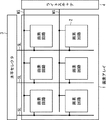
- 239000011159 matrix material Substances 0.000 description 6
- 239000008186 active pharmaceutical agent Substances 0.000 description 4
- 230000005669 field effect Effects 0.000 description 2
- 229910021420 polycrystalline silicon Inorganic materials 0.000 description 2
- 229920005591 polysilicon Polymers 0.000 description 2
- 239000004065 semiconductor Substances 0.000 description 2
- 229910021417 amorphous silicon Inorganic materials 0.000 description 1
- 230000005540 biological transmission Effects 0.000 description 1
- 239000003086 colorant Substances 0.000 description 1
- 230000007423 decrease Effects 0.000 description 1
- 238000001514 detection method Methods 0.000 description 1
- 238000005516 engineering process Methods 0.000 description 1
- 230000001771 impaired effect Effects 0.000 description 1
- 239000000758 substrate Substances 0.000 description 1
Images


Abstract
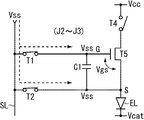
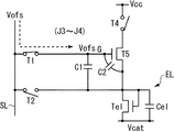
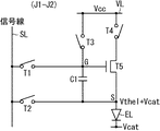
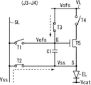
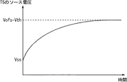
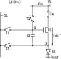
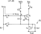
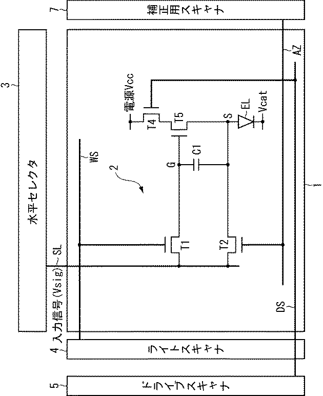
【解決手段】 画素回路2は、ドライブトランジスタT5のゲートGとソースS間に画素容量C1が接続され、ソースSとカソード電位Vcat間に発光素子ELが接続され、ゲートGと信号線SLとの間にサンプリングトランジスタT1が接続され、ゲートGと電源VLとの間に第1スイッチングトランジスタT3が接続され、ドレインDと電源VLとの間に第2スイッチングトランジスタT4が接続され、ソースSと信号線SLとの間に第3スイッチングトランジスタT2が接続されている。第1、第2及び第3スイッチングトランジスタT3,T4,T2は、映像信号Vsigが画素容量C1にサンプリングされる前に動作し、ドライブトランジスタT5の閾電圧Vthを検出して画素容量C1に書き込み、以って出力電流Idsの閾電圧Vthに対する依存性を補正する。
【選択図】図15
Description
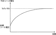
Ids=(1/2)μ(W/L)Cox(Vgs−Vth)2・・・式1
このトランジスタ特性式1において、Idsはソース/ドレイン間に流れるドレイン電流を表わしており、画素回路では発光素子に供給される出力電流である。Vgsはソースを基準としてゲートに印加されるゲート電圧を表わしており、画素回路では上述した入力電圧である。Vthはトランジスタの閾電圧である。又μはトランジスタのチャネルを構成する半導体薄膜の移動度を表わしている。その他Wはチャネル幅を表わし、Lはチャネル長を表わし、Coxはゲート容量を表わしている。このトランジスタ特性式1から明らかな様に、薄膜トランジスタは飽和領域で動作する時、ゲート電圧Vgsが閾電圧Vthを超えて大きくなると、オン状態となってドレイン電流Idsが流れる。原理的に見ると上記のトランジスタ特性式1が示す様に、ゲート電圧Vgsが一定であれば常に同じ量のドレイン電流Idsが発光素子に供給される。従って、画面を構成する各画素に全て同一のレベルの映像信号を供給すれば、全画素が同一輝度で発光し、画面の一様性(ユニフォーミティ)が得られるはずである。
Claims (12)
- 信号線と所要数の走査線が交差する部分に配され、発光素子とこれを駆動するドライブトランジスタとを含む画素回路であって、
該ドライブトランジスタのゲートとソース間に画素容量が接続され、該ドライブトランジスタのソースと所定のカソード電位間に該発光素子が接続され、該ドライブトランジスタのゲートと信号線との間にサンプリングトランジスタが接続され、該ドライブトランジスタのゲートと電源との間に第1スイッチングトランジスタが接続され、該ドライブトランジスタのドレインと電源との間に第2スイッチングトランジスタが接続され、該ドライブトランジスタのソースと信号線との間に第3スイッチングトランジスタが接続されており、
前記サンプリングトランジスタは、水平走査期間に導通して該信号線から供給された映像信号を該画素容量にサンプリングし、
前記画素容量は、該サンプリングされた映像信号に応じて該ドライブトランジスタのゲートに入力電圧を印加し、
前記ドライブトランジスタは、該入力電圧に応じた出力電流を該発光素子に供給し、該出力電流は該ドライブトランジスタの閾電圧に対して依存性を有し、
前記発光素子は、該ドライブトランジスタから供給された出力電流により該映像信号に応じた輝度で発光し、
前記第1、第2及び第3スイッチングトランジスタは、該映像信号が該画素容量にサンプリングされる前に動作し、該ドライブトランジスタの閾電圧を検出して該画素容量に書き込み、以って該出力電流の閾電圧に対する依存性を補正することを特徴とする画素回路。 - 前記第3スイッチングトランジスタがオフした後前記第1スイッチングトランジスタがオンしている状態で、前記第2スイッチトランジスタをオンオフ制御して、該ドライブトランジスタの閾電圧を検出しこれを該画素容量に書き込み、以って出力電流の該閾電圧に対する依存性を補正することを特徴とする請求項1記載の画素回路。
- 前記第2スイッチングトランジスタがオンしている時間幅は、該水平走査期間の時間幅よりも長く設定されていることを特徴とする請求項2記載の画素回路。
- 該ドライブトランジスタのゲートが第1スイッチングトランジスタを介して接続している電源と、該ドライブトランジスタのドレインが第2スイッチングトランジスタを介して接続している電源は、共通の電源ラインを通して電源電圧を供給することを特徴とする請求項1記載の画素回路。
- 前記共通の電源ラインは走査線と並行に配され、走査線と同様に走査されて時分割的に異なるレベルの電源電圧を供給することを特徴とする請求項4記載の画素回路。
- 前記電源電圧は、該発光素子が発光する期間に該ドライブトランジスタのドレインに供給される第1のレベルと、出力電流の閾電圧に対する依存性を補正する時に該ドライブトランジスタのゲートに与えられる第2のレベルとの間で切り替わることを特徴とする請求項5記載の画素回路。
- 該ドライブトランジスタのゲートが第1スイッチングトランジスタを介して接続している電源と、該ドライブトランジスタのドレインが第2スイッチングトランジスタを介して接続している電源は、別々に配された第1電源ライン及び第2電源ラインを通して異なるレベルの電源電圧を供給することを特徴とする請求項1記載の画素回路。
- 前記第1電源ラインは、出力電流の閾電圧に対する依存性を補正する時に必要なレベルの電源電圧を該ドライブトランジスタのゲートに供給し、前記第2電源ラインは、該発光素子が発光する期間に必要なレベルの電源電圧を該ドライブトランジスタのドレインに供給することを特徴とする請求項7記載の画素回路。
- 前記信号線は、映像信号を表す信号電圧と、一定のレベルに固定された固定電圧とを切り替えて供給することを特徴とする請求項1記載の画素回路。
- 前記サンプリングトランジスタは該水平走査期間に信号線から該信号電圧をサンプリングして画素容量に書き込む一方、
前記第3スイッチングトランジスタは、該水平走査期間よりも前で出力電流の閾電圧に対する依存性を補正する時の準備として、信号線から該固定電圧を該ドライブトランジスタのソースに充電することを特徴とする請求項9記載の画素回路。 - 前記第3スイッチングトランジスタは、当該走査線に割り当てられた水平走査期間に先行する他の走査線に割り当てられた前の水平走査期間で導通し、信号線から該固定電圧を該ドライブトランジスタのソースに充電することを特徴とする請求項10記載の画素回路。
- 前記第3トランジスタは、先行する他の複数の走査線に割り当てられた複数の水平走査期間で繰り返し導通し、信号線から該固定電圧を該ドライブトランジスタのソースに充電することを特徴とする請求項11記載の画素回路。
Priority Applications (1)
| Application Number | Priority Date | Filing Date | Title |
|---|---|---|---|
| JP2005336592A JP2007140318A (ja) | 2005-11-22 | 2005-11-22 | 画素回路 |
Applications Claiming Priority (1)
| Application Number | Priority Date | Filing Date | Title |
|---|---|---|---|
| JP2005336592A JP2007140318A (ja) | 2005-11-22 | 2005-11-22 | 画素回路 |
Publications (1)
| Publication Number | Publication Date |
|---|---|
| JP2007140318A true JP2007140318A (ja) | 2007-06-07 |
Family
ID=38203226
Family Applications (1)
| Application Number | Title | Priority Date | Filing Date |
|---|---|---|---|
| JP2005336592A Pending JP2007140318A (ja) | 2005-11-22 | 2005-11-22 | 画素回路 |
Country Status (1)
| Country | Link |
|---|---|
| JP (1) | JP2007140318A (ja) |
Cited By (22)
| Publication number | Priority date | Publication date | Assignee | Title |
|---|---|---|---|---|
| JP2009104013A (ja) * | 2007-10-25 | 2009-05-14 | Sony Corp | 表示装置、表示装置の駆動方法および電子機器 |
| JP2009128700A (ja) * | 2007-11-26 | 2009-06-11 | Sony Corp | 表示装置及びその駆動方法と電子機器 |
| JP2009204881A (ja) * | 2008-02-28 | 2009-09-10 | Sony Corp | El表示パネルモジュール、el表示パネル、集積回路装置、電子機器及び駆動制御方法 |
| JP2009271320A (ja) * | 2008-05-08 | 2009-11-19 | Sony Corp | El表示パネル、電子機器及びel表示パネルの駆動方法 |
| US8242983B2 (en) | 2008-06-11 | 2012-08-14 | Samsung Mobile Display Co., Ltd. | Pixel and organic light emitting display device using the same |
| US8345039B2 (en) | 2008-12-05 | 2013-01-01 | Samsung Display Co., Ltd. | Organic light emitting display device and method of driving the same |
| US8368618B2 (en) | 2008-12-19 | 2013-02-05 | Samsung Display Co., Ltd. | Organic light emitting display device |
| JP2013068957A (ja) * | 2012-11-08 | 2013-04-18 | Sony Corp | 表示装置 |
| US8531358B2 (en) | 2009-03-26 | 2013-09-10 | Samsung Display Co., Ltd. | Organic light emitting display device having improved brightness |
| US8654041B2 (en) | 2008-11-26 | 2014-02-18 | Samsung Display Co., Ltd. | Organic light emitting display device having more uniform luminance and method of driving the same |
| JP2014038334A (ja) * | 2005-12-02 | 2014-02-27 | Semiconductor Energy Lab Co Ltd | 半導体装置 |
| US8665182B2 (en) | 2009-01-29 | 2014-03-04 | Samsung Display Co., Ltd. | Emission control driver and organic light emitting display device using the same |
| US8669923B2 (en) | 2010-02-09 | 2014-03-11 | Samsung Display Co., Ltd. | Pixel and organic light emitting display device using the same |
| CN103730089A (zh) * | 2013-12-26 | 2014-04-16 | 京东方科技集团股份有限公司 | 栅极驱动电路、方法、阵列基板行驱动电路和显示装置 |
| US8830219B2 (en) | 2009-10-19 | 2014-09-09 | Samsung Display Co., Ltd. | Organic light emitting display device capable of compensating threshold voltage of a driving transistor and driving method thereof |
| KR101491152B1 (ko) | 2008-09-26 | 2015-02-09 | 엘지디스플레이 주식회사 | 유기발광다이오드 표시장치 |
| CN104778917A (zh) * | 2015-01-30 | 2015-07-15 | 京东方科技集团股份有限公司 | 像素驱动电路及其驱动方法和显示设备 |
| JP2015138154A (ja) * | 2014-01-22 | 2015-07-30 | セイコーエプソン株式会社 | 発光装置、及び電子機器 |
| WO2015132834A1 (ja) * | 2014-03-06 | 2015-09-11 | 株式会社Joled | 有機el表示装置 |
| US9536476B2 (en) | 2013-12-24 | 2017-01-03 | Boe Technology Group Co., Ltd. | Gate driver circuit, gate driving method, gate-on-array circuit, display device, and electronic product |
| JP2017500617A (ja) * | 2014-01-10 | 2017-01-05 | 深▲セン▼市華星光電技術有限公司 | 有機発光ダイオードの駆動回路 |
| US9620061B2 (en) | 2013-12-30 | 2017-04-11 | Boe Technology Group Co., Ltd. | Gate driver circuit, gate driving method, gate-on-array circuit, display device, and electronic product |
Citations (5)
| Publication number | Priority date | Publication date | Assignee | Title |
|---|---|---|---|---|
| JP2004246204A (ja) * | 2003-02-14 | 2004-09-02 | Sony Corp | 画素回路、表示装置、および画素回路の駆動方法 |
| JP2004361640A (ja) * | 2003-06-04 | 2004-12-24 | Sony Corp | 画素回路、表示装置、および画素回路の駆動方法 |
| JP2005128521A (ja) * | 2003-09-30 | 2005-05-19 | Sanyo Electric Co Ltd | 有機el画素回路 |
| JP2005202255A (ja) * | 2004-01-19 | 2005-07-28 | Sony Corp | 表示装置及びその駆動方法 |
| JP2007047633A (ja) * | 2005-08-12 | 2007-02-22 | Seiko Epson Corp | プリチャージ電圧生成方法、電気光学装置及び電子機器 |
-
2005
- 2005-11-22 JP JP2005336592A patent/JP2007140318A/ja active Pending
Patent Citations (5)
| Publication number | Priority date | Publication date | Assignee | Title |
|---|---|---|---|---|
| JP2004246204A (ja) * | 2003-02-14 | 2004-09-02 | Sony Corp | 画素回路、表示装置、および画素回路の駆動方法 |
| JP2004361640A (ja) * | 2003-06-04 | 2004-12-24 | Sony Corp | 画素回路、表示装置、および画素回路の駆動方法 |
| JP2005128521A (ja) * | 2003-09-30 | 2005-05-19 | Sanyo Electric Co Ltd | 有機el画素回路 |
| JP2005202255A (ja) * | 2004-01-19 | 2005-07-28 | Sony Corp | 表示装置及びその駆動方法 |
| JP2007047633A (ja) * | 2005-08-12 | 2007-02-22 | Seiko Epson Corp | プリチャージ電圧生成方法、電気光学装置及び電子機器 |
Cited By (36)
| Publication number | Priority date | Publication date | Assignee | Title |
|---|---|---|---|---|
| JP2014038334A (ja) * | 2005-12-02 | 2014-02-27 | Semiconductor Energy Lab Co Ltd | 半導体装置 |
| US8890180B2 (en) | 2005-12-02 | 2014-11-18 | Semiconductor Energy Laboratory Co., Ltd. | Semiconductor device, display device, and electronic device |
| US9997584B2 (en) | 2005-12-02 | 2018-06-12 | Semiconductor Energy Laboratory Co., Ltd. | Semiconductor device, display device, and electronic device |
| US11417720B2 (en) | 2005-12-02 | 2022-08-16 | Semiconductor Energy Laboratory Co., Ltd. | Display device including n-channel transistor including polysilicon |
| JP2018087981A (ja) * | 2005-12-02 | 2018-06-07 | 株式会社半導体エネルギー研究所 | 半導体装置 |
| US8217862B2 (en) | 2007-10-25 | 2012-07-10 | Sony Corporation | Display apparatus, driving method for display apparatus and electronic apparatus |
| JP2009104013A (ja) * | 2007-10-25 | 2009-05-14 | Sony Corp | 表示装置、表示装置の駆動方法および電子機器 |
| JP2009128700A (ja) * | 2007-11-26 | 2009-06-11 | Sony Corp | 表示装置及びその駆動方法と電子機器 |
| JP2009204881A (ja) * | 2008-02-28 | 2009-09-10 | Sony Corp | El表示パネルモジュール、el表示パネル、集積回路装置、電子機器及び駆動制御方法 |
| US8384626B2 (en) | 2008-02-28 | 2013-02-26 | Sony Corporation | EL display panel module, EL display panel, integrated circuit device, electronic apparatus and driving controlling method |
| US8982018B2 (en) | 2008-02-28 | 2015-03-17 | Sony Corporation | EL display panel module, EL display panel, integrated circuit device, electronic apparatus and driving controlling method |
| TWI417837B (zh) * | 2008-02-28 | 2013-12-01 | Sony Corp | 電致發光顯示面板模組,電致發光顯示面板,積體電路裝置,電子設備及驅動控制方法 |
| KR101557293B1 (ko) | 2008-05-08 | 2015-10-06 | 가부시키가이샤 제이올레드 | El 표시 패널 |
| JP2009271320A (ja) * | 2008-05-08 | 2009-11-19 | Sony Corp | El表示パネル、電子機器及びel表示パネルの駆動方法 |
| US8242983B2 (en) | 2008-06-11 | 2012-08-14 | Samsung Mobile Display Co., Ltd. | Pixel and organic light emitting display device using the same |
| KR101491152B1 (ko) | 2008-09-26 | 2015-02-09 | 엘지디스플레이 주식회사 | 유기발광다이오드 표시장치 |
| US8654041B2 (en) | 2008-11-26 | 2014-02-18 | Samsung Display Co., Ltd. | Organic light emitting display device having more uniform luminance and method of driving the same |
| US8345039B2 (en) | 2008-12-05 | 2013-01-01 | Samsung Display Co., Ltd. | Organic light emitting display device and method of driving the same |
| US8368618B2 (en) | 2008-12-19 | 2013-02-05 | Samsung Display Co., Ltd. | Organic light emitting display device |
| US8665182B2 (en) | 2009-01-29 | 2014-03-04 | Samsung Display Co., Ltd. | Emission control driver and organic light emitting display device using the same |
| US8531358B2 (en) | 2009-03-26 | 2013-09-10 | Samsung Display Co., Ltd. | Organic light emitting display device having improved brightness |
| US8830219B2 (en) | 2009-10-19 | 2014-09-09 | Samsung Display Co., Ltd. | Organic light emitting display device capable of compensating threshold voltage of a driving transistor and driving method thereof |
| US8669923B2 (en) | 2010-02-09 | 2014-03-11 | Samsung Display Co., Ltd. | Pixel and organic light emitting display device using the same |
| JP2013068957A (ja) * | 2012-11-08 | 2013-04-18 | Sony Corp | 表示装置 |
| US9536476B2 (en) | 2013-12-24 | 2017-01-03 | Boe Technology Group Co., Ltd. | Gate driver circuit, gate driving method, gate-on-array circuit, display device, and electronic product |
| CN103730089B (zh) * | 2013-12-26 | 2015-11-25 | 京东方科技集团股份有限公司 | 栅极驱动电路、方法、阵列基板行驱动电路和显示装置 |
| US9514683B2 (en) | 2013-12-26 | 2016-12-06 | Boe Technology Group Co., Ltd. | Gate driving circuit, gate driving method, gate on array (GOA) circuit and display device |
| CN103730089A (zh) * | 2013-12-26 | 2014-04-16 | 京东方科技集团股份有限公司 | 栅极驱动电路、方法、阵列基板行驱动电路和显示装置 |
| US9620061B2 (en) | 2013-12-30 | 2017-04-11 | Boe Technology Group Co., Ltd. | Gate driver circuit, gate driving method, gate-on-array circuit, display device, and electronic product |
| JP2017500617A (ja) * | 2014-01-10 | 2017-01-05 | 深▲セン▼市華星光電技術有限公司 | 有機発光ダイオードの駆動回路 |
| KR101841861B1 (ko) * | 2014-01-10 | 2018-03-23 | 센젠 차이나 스타 옵토일렉트로닉스 테크놀로지 컴퍼니 리미티드 | 유기발광 다이오드의 구동회로 |
| JP2015138154A (ja) * | 2014-01-22 | 2015-07-30 | セイコーエプソン株式会社 | 発光装置、及び電子機器 |
| WO2015132834A1 (ja) * | 2014-03-06 | 2015-09-11 | 株式会社Joled | 有機el表示装置 |
| JPWO2015132834A1 (ja) * | 2014-03-06 | 2017-03-30 | 株式会社Joled | 有機el表示装置 |
| US9916788B2 (en) | 2014-03-06 | 2018-03-13 | Joled Inc. | Organic electroluminescent display device |
| CN104778917A (zh) * | 2015-01-30 | 2015-07-15 | 京东方科技集团股份有限公司 | 像素驱动电路及其驱动方法和显示设备 |
Similar Documents
| Publication | Publication Date | Title |
|---|---|---|
| US11170721B2 (en) | Pixel circuit and display apparatus | |
| US8907875B1 (en) | Pixel circuit, display and driving method thereof | |
| JP2007140318A (ja) | 画素回路 | |
| KR101200066B1 (ko) | 화소회로, 액티브 매트릭스 장치 및 표시장치 | |
| JP4300490B2 (ja) | 表示装置及びその駆動方法と電子機器 | |
| JP4923527B2 (ja) | 表示装置及びその駆動方法 | |
| JP2007148129A (ja) | 表示装置及びその駆動方法 | |
| JP4983018B2 (ja) | 表示装置及びその駆動方法 | |
| JP2007148128A (ja) | 画素回路 | |
| JP4929891B2 (ja) | 表示装置 | |
| JP2008287139A (ja) | 表示装置及びその駆動方法と電子機器 | |
| JP2006133542A (ja) | 画素回路及び表示装置 | |
| JP2006215275A (ja) | 表示装置 | |
| JP2006154521A (ja) | 画素回路と表示装置及びこれらの駆動方法 | |
| JP2006227238A (ja) | 表示装置、表示方法 | |
| JP4706288B2 (ja) | 画素回路及び表示装置 | |
| JP2006227239A (ja) | 表示装置、表示方法 | |
| JP2007316453A (ja) | 画像表示装置 | |
| JP2008026468A (ja) | 画像表示装置 | |
| JP5282355B2 (ja) | 画像表示装置 | |
| JP2006243525A (ja) | 表示装置 | |
| JP2006208746A (ja) | 画素回路と表示装置及びこれらの駆動方法 | |
| JP2006038965A (ja) | 画素回路及び表示装置とこれらの駆動方法 | |
| JP2012088724A (ja) | 画素回路および表示装置 | |
| JP2008065199A (ja) | 表示装置及びその製造方法 |
Legal Events
| Date | Code | Title | Description |
|---|---|---|---|
| A621 | Written request for application examination |
Free format text: JAPANESE INTERMEDIATE CODE: A621 Effective date: 20081117 |
|
| A521 | Request for written amendment filed |
Free format text: JAPANESE INTERMEDIATE CODE: A821 Effective date: 20090223 |
|
| RD02 | Notification of acceptance of power of attorney |
Free format text: JAPANESE INTERMEDIATE CODE: A7422 Effective date: 20090223 |
|
| RD05 | Notification of revocation of power of attorney |
Free format text: JAPANESE INTERMEDIATE CODE: A7425 Effective date: 20090226 |
|
| A131 | Notification of reasons for refusal |
Free format text: JAPANESE INTERMEDIATE CODE: A131 Effective date: 20110726 |
|
| A02 | Decision of refusal |
Free format text: JAPANESE INTERMEDIATE CODE: A02 Effective date: 20120207 |