JP2006332247A - 電源装置および電気装置の放熱構造 - Google Patents
電源装置および電気装置の放熱構造 Download PDFInfo
- Publication number
- JP2006332247A JP2006332247A JP2005152393A JP2005152393A JP2006332247A JP 2006332247 A JP2006332247 A JP 2006332247A JP 2005152393 A JP2005152393 A JP 2005152393A JP 2005152393 A JP2005152393 A JP 2005152393A JP 2006332247 A JP2006332247 A JP 2006332247A
- Authority
- JP
- Japan
- Prior art keywords
- printed circuit
- circuit board
- semiconductor element
- flexible
- solder connection
- Prior art date
- Legal status (The legal status is an assumption and is not a legal conclusion. Google has not performed a legal analysis and makes no representation as to the accuracy of the status listed.)
- Pending
Links
Images


Classifications
-
- H—ELECTRICITY
- H05—ELECTRIC TECHNIQUES NOT OTHERWISE PROVIDED FOR
- H05K—PRINTED CIRCUITS; CASINGS OR CONSTRUCTIONAL DETAILS OF ELECTRIC APPARATUS; MANUFACTURE OF ASSEMBLAGES OF ELECTRICAL COMPONENTS
- H05K1/00—Printed circuits
- H05K1/02—Details
- H05K1/0271—Arrangements for reducing stress or warp in rigid printed circuit boards, e.g. caused by loads, vibrations or differences in thermal expansion
-
- H—ELECTRICITY
- H01—ELECTRIC ELEMENTS
- H01L—SEMICONDUCTOR DEVICES NOT COVERED BY CLASS H10
- H01L23/00—Details of semiconductor or other solid state devices
- H01L23/34—Arrangements for cooling, heating, ventilating or temperature compensation ; Temperature sensing arrangements
- H01L23/40—Mountings or securing means for detachable cooling or heating arrangements ; fixed by friction, plugs or springs
- H01L23/4006—Mountings or securing means for detachable cooling or heating arrangements ; fixed by friction, plugs or springs with bolts or screws
- H01L2023/4018—Mountings or securing means for detachable cooling or heating arrangements ; fixed by friction, plugs or springs with bolts or screws characterised by the type of device to be heated or cooled
- H01L2023/4031—Packaged discrete devices, e.g. to-3 housings, diodes
-
- H—ELECTRICITY
- H01—ELECTRIC ELEMENTS
- H01L—SEMICONDUCTOR DEVICES NOT COVERED BY CLASS H10
- H01L23/00—Details of semiconductor or other solid state devices
- H01L23/34—Arrangements for cooling, heating, ventilating or temperature compensation ; Temperature sensing arrangements
- H01L23/36—Selection of materials, or shaping, to facilitate cooling or heating, e.g. heatsinks
- H01L23/367—Cooling facilitated by shape of device
-
- H—ELECTRICITY
- H01—ELECTRIC ELEMENTS
- H01L—SEMICONDUCTOR DEVICES NOT COVERED BY CLASS H10
- H01L23/00—Details of semiconductor or other solid state devices
- H01L23/34—Arrangements for cooling, heating, ventilating or temperature compensation ; Temperature sensing arrangements
- H01L23/40—Mountings or securing means for detachable cooling or heating arrangements ; fixed by friction, plugs or springs
- H01L23/4006—Mountings or securing means for detachable cooling or heating arrangements ; fixed by friction, plugs or springs with bolts or screws
-
- H—ELECTRICITY
- H01—ELECTRIC ELEMENTS
- H01L—SEMICONDUCTOR DEVICES NOT COVERED BY CLASS H10
- H01L25/00—Assemblies consisting of a plurality of individual semiconductor or other solid state devices ; Multistep manufacturing processes thereof
- H01L25/03—Assemblies consisting of a plurality of individual semiconductor or other solid state devices ; Multistep manufacturing processes thereof all the devices being of a type provided for in the same subgroup of groups H01L27/00 - H01L33/00, or in a single subclass of H10K, H10N, e.g. assemblies of rectifier diodes
- H01L25/10—Assemblies consisting of a plurality of individual semiconductor or other solid state devices ; Multistep manufacturing processes thereof all the devices being of a type provided for in the same subgroup of groups H01L27/00 - H01L33/00, or in a single subclass of H10K, H10N, e.g. assemblies of rectifier diodes the devices having separate containers
- H01L25/11—Assemblies consisting of a plurality of individual semiconductor or other solid state devices ; Multistep manufacturing processes thereof all the devices being of a type provided for in the same subgroup of groups H01L27/00 - H01L33/00, or in a single subclass of H10K, H10N, e.g. assemblies of rectifier diodes the devices having separate containers the devices being of a type provided for in group H01L29/00
- H01L25/115—Assemblies consisting of a plurality of individual semiconductor or other solid state devices ; Multistep manufacturing processes thereof all the devices being of a type provided for in the same subgroup of groups H01L27/00 - H01L33/00, or in a single subclass of H10K, H10N, e.g. assemblies of rectifier diodes the devices having separate containers the devices being of a type provided for in group H01L29/00 the devices being arranged next to each other
-
- H—ELECTRICITY
- H01—ELECTRIC ELEMENTS
- H01L—SEMICONDUCTOR DEVICES NOT COVERED BY CLASS H10
- H01L2924/00—Indexing scheme for arrangements or methods for connecting or disconnecting semiconductor or solid-state bodies as covered by H01L24/00
- H01L2924/0001—Technical content checked by a classifier
- H01L2924/0002—Not covered by any one of groups H01L24/00, H01L24/00 and H01L2224/00
-
- H—ELECTRICITY
- H05—ELECTRIC TECHNIQUES NOT OTHERWISE PROVIDED FOR
- H05K—PRINTED CIRCUITS; CASINGS OR CONSTRUCTIONAL DETAILS OF ELECTRIC APPARATUS; MANUFACTURE OF ASSEMBLAGES OF ELECTRICAL COMPONENTS
- H05K1/00—Printed circuits
- H05K1/02—Details
- H05K1/0201—Thermal arrangements, e.g. for cooling, heating or preventing overheating
- H05K1/0203—Cooling of mounted components
-
- H—ELECTRICITY
- H05—ELECTRIC TECHNIQUES NOT OTHERWISE PROVIDED FOR
- H05K—PRINTED CIRCUITS; CASINGS OR CONSTRUCTIONAL DETAILS OF ELECTRIC APPARATUS; MANUFACTURE OF ASSEMBLAGES OF ELECTRICAL COMPONENTS
- H05K2201/00—Indexing scheme relating to printed circuits covered by H05K1/00
- H05K2201/09—Shape and layout
- H05K2201/09009—Substrate related
- H05K2201/09036—Recesses or grooves in insulating substrate
-
- H—ELECTRICITY
- H05—ELECTRIC TECHNIQUES NOT OTHERWISE PROVIDED FOR
- H05K—PRINTED CIRCUITS; CASINGS OR CONSTRUCTIONAL DETAILS OF ELECTRIC APPARATUS; MANUFACTURE OF ASSEMBLAGES OF ELECTRICAL COMPONENTS
- H05K2201/00—Indexing scheme relating to printed circuits covered by H05K1/00
- H05K2201/10—Details of components or other objects attached to or integrated in a printed circuit board
- H05K2201/10007—Types of components
- H05K2201/10166—Transistor
-
- H—ELECTRICITY
- H05—ELECTRIC TECHNIQUES NOT OTHERWISE PROVIDED FOR
- H05K—PRINTED CIRCUITS; CASINGS OR CONSTRUCTIONAL DETAILS OF ELECTRIC APPARATUS; MANUFACTURE OF ASSEMBLAGES OF ELECTRICAL COMPONENTS
- H05K2201/00—Indexing scheme relating to printed circuits covered by H05K1/00
- H05K2201/10—Details of components or other objects attached to or integrated in a printed circuit board
- H05K2201/10431—Details of mounted components
- H05K2201/10439—Position of a single component
- H05K2201/10446—Mounted on an edge
-
- H—ELECTRICITY
- H05—ELECTRIC TECHNIQUES NOT OTHERWISE PROVIDED FOR
- H05K—PRINTED CIRCUITS; CASINGS OR CONSTRUCTIONAL DETAILS OF ELECTRIC APPARATUS; MANUFACTURE OF ASSEMBLAGES OF ELECTRICAL COMPONENTS
- H05K3/00—Apparatus or processes for manufacturing printed circuits
- H05K3/30—Assembling printed circuits with electric components, e.g. with resistor
- H05K3/32—Assembling printed circuits with electric components, e.g. with resistor electrically connecting electric components or wires to printed circuits
- H05K3/34—Assembling printed circuits with electric components, e.g. with resistor electrically connecting electric components or wires to printed circuits by soldering
- H05K3/3447—Lead-in-hole components
Abstract
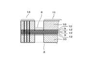
【解決手段】半導体素子駆動用プリント基板3において,半導体素子のリード端子5との半田接続部13と半田接続部以外の部分11との間にフレキシブル部8を形成し,フレキシブル部8はプリント基板の表面・裏面を構成しているガラスエポキシ材などの絶縁基材10を実装しないことにより,銅箔9と銅箔間の絶縁物12とで薄いフィルム状のフレキシブル性を有する状態とし,半導体素子のリード端子5にかかる歪力あるいは振動による動荷重を吸収できるようにする。
【選択図】 図1
Description
2 半導体素子冷却フィン
3 半導体素子駆動用プリント基板
4 制御用基板
5 半導体素子のリード端子
6 半導体素子のリード端子の半導体駆動用プリント基板への半田接続部
7 出力制御ブロック
8 フレキシブル部
9 銅箔
10 絶縁基材
11 半田接続部以外の部分
12 銅箔間の絶縁物
13 半導体素子のリード端子と半田接続する半導体素子駆動用プリント基板の半田接
続部
14 部品
15 リード端子
16 プリント基板
17 フレキシブル基板
18 抑え金具
Claims (5)
- 半導体素子と半導体素子冷却フィンとプリント基板などが一体のブロック構造に組み立てられ,半導体素子駆動用プリント基板に半導体素子のリード端子が直接半田付けされている溶接機用,めっき用などの電源装置において,前記プリント基板の前記半田付け部の周辺がフレキシブル性を有する材料を用いて構成されるプリント基板にした事を特徴とする電源装置の放熱構造。
- 請求項1の電源装置において,前記の半田付け部がフレキシブル性を有する材料を用いて構成される前記プリント基板は,半導体素子のリード端子との半田接続部と前記の半田接続部以外の部分との間を薄いフィルム状のフレキシブル部としたことを特徴とする電源装置の放熱構造。
- 請求項2の電源装置において,前記プリント基板の半田接続部と,前記プリント基板の半田接続部以外の部分との間を薄いフィルム状のフレキシブル部とする,前記プリント基板は,その表面と裏面を構成しているガラスエポキシ材などの絶縁基材を,前記フレキシブル部とする部分には実装しないことにより,銅箔で,あるいは多層基板の場合は銅箔と銅箔間の絶縁材とで薄いフィルム状のフレキシブル部を構成することを特徴とする電源装置の放熱構造。
- プリント基板を内部に備え,前記プリント基板外から剛性の配線を前記プリント基板に半田接続する電気装置において,前記プリント基板の半田接続部と前記プリント基板の半田接続部以外の部分との間を薄いフィルム状のフレキシブル部とし,前記プリント基板の表面と裏面を構成しているガラスエポキシ材などの絶縁基材を,前記フレキシブル部とする部分には実装しないことにより,銅箔で,あるいは多層基板の場合は銅箔と銅箔間の絶縁材とで薄いフィルム状のフレキシブル部を構成することを特徴とする電気装置の放熱構造。
- プリント基板を内部に備え,前記プリント基板外から剛性の配線を前記プリント基板に接続する電気装置において,前記プリント基板の前記接続部と前記プリント基板の前記接続部以外の部分との間を薄いフィルム状のフレキシブル部とし,前記プリント基板の表面と裏面を構成しているガラスエポキシ材などの絶縁基材を,前記フレキシブル部とする部分には実装しないことにより,銅箔で,あるいは多層基板の場合は銅箔と銅箔間の絶縁材とで薄いフィルム状のフレキシブル部を構成することを特徴とする電気装置
の放熱構造。
Priority Applications (4)
| Application Number | Priority Date | Filing Date | Title |
|---|---|---|---|
| JP2005152393A JP2006332247A (ja) | 2005-05-25 | 2005-05-25 | 電源装置および電気装置の放熱構造 |
| US11/439,412 US7579554B2 (en) | 2005-05-25 | 2006-05-22 | Heat sink arrangement for electrical apparatus |
| CNB2006100996342A CN100562216C (zh) | 2005-05-25 | 2006-05-25 | 用于电气设备的散热装置 |
| US12/475,728 US7902464B2 (en) | 2005-05-25 | 2009-06-01 | Heat sink arrangement for electrical apparatus |
Applications Claiming Priority (1)
| Application Number | Priority Date | Filing Date | Title |
|---|---|---|---|
| JP2005152393A JP2006332247A (ja) | 2005-05-25 | 2005-05-25 | 電源装置および電気装置の放熱構造 |
Publications (1)
| Publication Number | Publication Date |
|---|---|
| JP2006332247A true JP2006332247A (ja) | 2006-12-07 |
Family
ID=37444380
Family Applications (1)
| Application Number | Title | Priority Date | Filing Date |
|---|---|---|---|
| JP2005152393A Pending JP2006332247A (ja) | 2005-05-25 | 2005-05-25 | 電源装置および電気装置の放熱構造 |
Country Status (3)
| Country | Link |
|---|---|
| US (2) | US7579554B2 (ja) |
| JP (1) | JP2006332247A (ja) |
| CN (1) | CN100562216C (ja) |
Cited By (2)
| Publication number | Priority date | Publication date | Assignee | Title |
|---|---|---|---|---|
| JP2010010630A (ja) * | 2008-06-30 | 2010-01-14 | Fujitsu Ltd | 基板ユニット及び基板及び電子装置 |
| JP2019091842A (ja) * | 2017-11-16 | 2019-06-13 | 矢崎総業株式会社 | 電子回路基板 |
Families Citing this family (4)
| Publication number | Priority date | Publication date | Assignee | Title |
|---|---|---|---|---|
| KR101182661B1 (ko) | 2011-05-27 | 2012-09-17 | 주식회사 유라코퍼레이션 | 인버터용 전력 모듈의 쿨링 팬 장치 |
| KR101182662B1 (ko) | 2011-05-27 | 2012-09-14 | 주식회사 유라코퍼레이션 | 인버터용 전력 모듈의 쿨링 팬 장치 |
| JP5663450B2 (ja) | 2011-10-18 | 2015-02-04 | 株式会社日立製作所 | 電力変換装置 |
| HK1210376A2 (en) | 2015-08-17 | 2016-04-15 | 馮文標 號 | Assembly structure of high-power semiconductor and heat sink |
Citations (3)
| Publication number | Priority date | Publication date | Assignee | Title |
|---|---|---|---|---|
| JPS63108675U (ja) * | 1986-12-27 | 1988-07-13 | ||
| JPH03241786A (ja) * | 1990-02-19 | 1991-10-28 | Aiwa Co Ltd | 機構部品のプリント基板への実装方法 |
| JPH07193370A (ja) * | 1993-12-25 | 1995-07-28 | Ibiden Co Ltd | フレックスリジッドプリント基板及びその製造方法 |
Family Cites Families (11)
| Publication number | Priority date | Publication date | Assignee | Title |
|---|---|---|---|---|
| IT1235830B (it) * | 1989-07-11 | 1992-11-03 | Sgs Thomson Microelectronics | Contenitore plastico single in line fornito di asole aperte sul lato opposto alla faccia dalla quale emergono i piedini per ricevere scorrevolmente altrettanti gambi di organi di fissaggio predisposti suun dissipatore esterno di calore |
| US4931134A (en) * | 1989-08-15 | 1990-06-05 | Parlex Corporation | Method of using laser routing to form a rigid/flex circuit board |
| DE4231140A1 (de) * | 1992-09-17 | 1994-03-24 | Bosch Gmbh Robert | Baugruppe für elektronische Steuergeräte |
| JPH077167U (ja) | 1993-06-29 | 1995-01-31 | 松下電工株式会社 | 電気部品実装構造 |
| DE19516947A1 (de) | 1995-05-11 | 1996-11-14 | Roeder Martin | Sitzgruppen-Element |
| US5998738A (en) * | 1996-08-30 | 1999-12-07 | Motorola Inc. | Electronic control module |
| DE69812570T2 (de) * | 1997-12-24 | 2004-01-29 | Denso Corp | Gerät mit Leiterplatte und dessen Zusammenbauverfahren |
| DE19924993C2 (de) * | 1999-05-31 | 2002-10-10 | Tyco Electronics Logistics Ag | Intelligentes Leistungsmodul in Sandwich-Bauweise |
| JP4142227B2 (ja) * | 2000-01-28 | 2008-09-03 | サンデン株式会社 | 車両用電動圧縮機のモータ駆動用インバータ装置 |
| WO2003049518A1 (fr) * | 2001-12-04 | 2003-06-12 | Tokyo R & D Co., Ltd. | Alimentation de courant |
| US6721189B1 (en) * | 2002-03-13 | 2004-04-13 | Rambus, Inc. | Memory module |
-
2005
- 2005-05-25 JP JP2005152393A patent/JP2006332247A/ja active Pending
-
2006
- 2006-05-22 US US11/439,412 patent/US7579554B2/en active Active
- 2006-05-25 CN CNB2006100996342A patent/CN100562216C/zh active Active
-
2009
- 2009-06-01 US US12/475,728 patent/US7902464B2/en active Active
Patent Citations (3)
| Publication number | Priority date | Publication date | Assignee | Title |
|---|---|---|---|---|
| JPS63108675U (ja) * | 1986-12-27 | 1988-07-13 | ||
| JPH03241786A (ja) * | 1990-02-19 | 1991-10-28 | Aiwa Co Ltd | 機構部品のプリント基板への実装方法 |
| JPH07193370A (ja) * | 1993-12-25 | 1995-07-28 | Ibiden Co Ltd | フレックスリジッドプリント基板及びその製造方法 |
Cited By (3)
| Publication number | Priority date | Publication date | Assignee | Title |
|---|---|---|---|---|
| JP2010010630A (ja) * | 2008-06-30 | 2010-01-14 | Fujitsu Ltd | 基板ユニット及び基板及び電子装置 |
| JP2019091842A (ja) * | 2017-11-16 | 2019-06-13 | 矢崎総業株式会社 | 電子回路基板 |
| US10764998B2 (en) | 2017-11-16 | 2020-09-01 | Yazaki Corporation | Electronic circuit board |
Also Published As
| Publication number | Publication date |
|---|---|
| US20060267180A1 (en) | 2006-11-30 |
| CN100562216C (zh) | 2009-11-18 |
| US20090237898A1 (en) | 2009-09-24 |
| US7902464B2 (en) | 2011-03-08 |
| CN1870858A (zh) | 2006-11-29 |
| US7579554B2 (en) | 2009-08-25 |
Similar Documents
| Publication | Publication Date | Title |
|---|---|---|
| JP2009117612A (ja) | 回路モジュールとその製造方法 | |
| JP2006210852A (ja) | 表面実装型回路部品を実装する回路基板及びその製造方法 | |
| JP2006332247A (ja) | 電源装置および電気装置の放熱構造 | |
| JP2011108924A (ja) | 熱伝導基板及びその電子部品実装方法 | |
| JP2013123011A (ja) | 電子装置 | |
| JP5169800B2 (ja) | 電子装置 | |
| JP2009016398A (ja) | プリント配線板構造、電子部品の実装方法および電子機器 | |
| JP2008028254A (ja) | 電子デバイスの放熱構造 | |
| WO2021053907A1 (ja) | 電子制御装置 | |
| JP2013247168A (ja) | 電源装置 | |
| JPH088372A (ja) | 放熱装置 | |
| JPH088373A (ja) | 放熱装置 | |
| JP2010003718A (ja) | 放熱基板とその製造方法及びこれを用いたモジュール | |
| JP2009076813A (ja) | 半導体装置 | |
| KR101281043B1 (ko) | 히트 싱크 | |
| JP2007088272A (ja) | セラミックス回路基板およびこれを用いたモジュール | |
| JP2013065887A (ja) | 電子装置 | |
| JP4770528B2 (ja) | 電子機器 | |
| JP4853276B2 (ja) | 半導体装置の製造方法 | |
| JP2018022764A (ja) | 電子装置 | |
| JP6403741B2 (ja) | 表面実装型半導体パッケージ装置 | |
| JP2011142142A (ja) | ヒートシンク取付構造及びヒートシンク取付方法 | |
| JP2010003972A (ja) | 電源モジュール | |
| JP2007123780A (ja) | 緩衝部を有する回路基板および製造方法 | |
| JP2023097018A (ja) | 電子制御装置及びその製造方法 |
Legal Events
| Date | Code | Title | Description |
|---|---|---|---|
| A621 | Written request for application examination |
Free format text: JAPANESE INTERMEDIATE CODE: A621 Effective date: 20080331 |
|
| RD02 | Notification of acceptance of power of attorney |
Free format text: JAPANESE INTERMEDIATE CODE: A7422 Effective date: 20080331 |
|
| A977 | Report on retrieval |
Free format text: JAPANESE INTERMEDIATE CODE: A971007 Effective date: 20100615 |
|
| A131 | Notification of reasons for refusal |
Free format text: JAPANESE INTERMEDIATE CODE: A131 Effective date: 20100622 |
|
| A02 | Decision of refusal |
Free format text: JAPANESE INTERMEDIATE CODE: A02 Effective date: 20101019 |