JP2007123780A - 緩衝部を有する回路基板および製造方法 - Google Patents
緩衝部を有する回路基板および製造方法 Download PDFInfo
- Publication number
- JP2007123780A JP2007123780A JP2005317617A JP2005317617A JP2007123780A JP 2007123780 A JP2007123780 A JP 2007123780A JP 2005317617 A JP2005317617 A JP 2005317617A JP 2005317617 A JP2005317617 A JP 2005317617A JP 2007123780 A JP2007123780 A JP 2007123780A
- Authority
- JP
- Japan
- Prior art keywords
- circuit board
- printed wiring
- buffer
- wiring board
- mounting hole
- Prior art date
- Legal status (The legal status is an assumption and is not a legal conclusion. Google has not performed a legal analysis and makes no representation as to the accuracy of the status listed.)
- Granted
Links
Images


Classifications
-
- H—ELECTRICITY
- H05—ELECTRIC TECHNIQUES NOT OTHERWISE PROVIDED FOR
- H05K—PRINTED CIRCUITS; CASINGS OR CONSTRUCTIONAL DETAILS OF ELECTRIC APPARATUS; MANUFACTURE OF ASSEMBLAGES OF ELECTRICAL COMPONENTS
- H05K2201/00—Indexing scheme relating to printed circuits covered by H05K1/00
- H05K2201/09—Shape and layout
- H05K2201/09818—Shape or layout details not covered by a single group of H05K2201/09009 - H05K2201/09809
- H05K2201/09909—Special local insulating pattern, e.g. as dam around component
-
- H—ELECTRICITY
- H05—ELECTRIC TECHNIQUES NOT OTHERWISE PROVIDED FOR
- H05K—PRINTED CIRCUITS; CASINGS OR CONSTRUCTIONAL DETAILS OF ELECTRIC APPARATUS; MANUFACTURE OF ASSEMBLAGES OF ELECTRICAL COMPONENTS
- H05K2201/00—Indexing scheme relating to printed circuits covered by H05K1/00
- H05K2201/10—Details of components or other objects attached to or integrated in a printed circuit board
- H05K2201/10227—Other objects, e.g. metallic pieces
- H05K2201/10409—Screws
Landscapes
- Electric Connection Of Electric Components To Printed Circuits (AREA)
- Structure Of Printed Boards (AREA)
Abstract
【解決手段】 プリント配線板に部品を実装しハンダ付けして回路基板を製造する工程内において、ソルダペーストの印刷工程の後に緩衝材塗布工程を設け、熱硬化する液状の材料をプリント配線板の取付け穴の周辺に塗布し、ハンダを加熱しハンダ付けする製造工程にて液状の材料を熱硬化させることによって緩衝部を形成する。
【選択図】 図1
Description
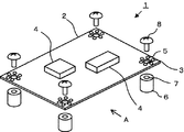
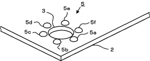
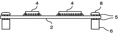
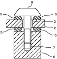
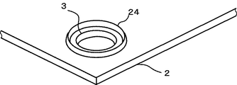
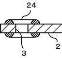
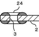
2 プリント配線板
3 取付け穴
4 部品
5 緩衝部
6 支持部
8 ねじ
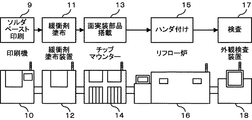
9 印刷工程
11 緩衝材塗布工程
13 面実装部品搭載工程
15 ハンダ付け工程
17 検査工程
24 緩衝部
Claims (6)
- 取付け穴を有するプリント配線板と、
前記プリント配線板に実装される部品と、
前記取付け穴の周辺に塗布された液状の材料が前記プリント配線板に前記部品を実装する際の加熱工程において熱硬化されて形成された緩衝部と
を有することを特徴とする回路基板。 - 前記緩衝部は、シリコン系ゴム材料によって形成され前記取付け穴の周辺に前記取り付け穴を囲むように配置された複数の半球状の緩衝部によって構成されたことを特徴とする請求項1記載の回路基板。
- 前記緩衝部は、シリコン系ゴム材料によって前記取付け穴の周辺に断面が半円の円環状に形成されていることを特徴とする請求項1記載の回路基板。
- 前記緩衝部は、導電性シリコン系ゴム材料によって形成され前記取付け穴の周辺に前記取り付け穴を囲むように配置された複数の半球状の緩衝部によって構成されていることを特徴とする請求項1記載の回路基板。
- 前記緩衝部は、導電性シリコン系ゴム材料によって前記取付け穴の周辺に断面が半円の円環状に形成されていることを特徴とする請求項1記載の回路基板。
- 取付け穴を有するプリント配線板に、部品を実装しハンダ付けする回路基板の製造方法において、
前記取付け穴の周辺に、熱硬化する液状の材料を前記取付け穴の周辺に塗布し、ハンダを加熱する製造工程でハンダを過熱すると共に前記材料を熱硬化させて緩衝部を形成することを特徴とする回路基板の製造方法。
Priority Applications (1)
| Application Number | Priority Date | Filing Date | Title |
|---|---|---|---|
| JP2005317617A JP4664802B2 (ja) | 2005-10-31 | 2005-10-31 | 回路基板、回路基板の製造方法および電子機器 |
Applications Claiming Priority (1)
| Application Number | Priority Date | Filing Date | Title |
|---|---|---|---|
| JP2005317617A JP4664802B2 (ja) | 2005-10-31 | 2005-10-31 | 回路基板、回路基板の製造方法および電子機器 |
Publications (2)
| Publication Number | Publication Date |
|---|---|
| JP2007123780A true JP2007123780A (ja) | 2007-05-17 |
| JP4664802B2 JP4664802B2 (ja) | 2011-04-06 |
Family
ID=38147251
Family Applications (1)
| Application Number | Title | Priority Date | Filing Date |
|---|---|---|---|
| JP2005317617A Expired - Fee Related JP4664802B2 (ja) | 2005-10-31 | 2005-10-31 | 回路基板、回路基板の製造方法および電子機器 |
Country Status (1)
| Country | Link |
|---|---|
| JP (1) | JP4664802B2 (ja) |
Cited By (2)
| Publication number | Priority date | Publication date | Assignee | Title |
|---|---|---|---|---|
| JP2010135622A (ja) * | 2008-12-05 | 2010-06-17 | Tokai Rika Co Ltd | 回路基板およびこの回路基板を備えた電子機器 |
| EP4192204A1 (en) * | 2021-12-02 | 2023-06-07 | Aptiv Technologies Limited | Integrated flexible circuit attachment features with sound dampening and method of forming said features |
Citations (5)
| Publication number | Priority date | Publication date | Assignee | Title |
|---|---|---|---|---|
| JPS55109121U (ja) * | 1979-01-27 | 1980-07-31 | ||
| JPS6224116U (ja) * | 1985-07-29 | 1987-02-14 | ||
| JPH1154963A (ja) * | 1997-07-29 | 1999-02-26 | Fujitsu Ten Ltd | 電子機器の取付構造 |
| JPH11177016A (ja) * | 1997-12-15 | 1999-07-02 | Denso Corp | 混成集積回路装置 |
| JPH11330640A (ja) * | 1998-05-18 | 1999-11-30 | Seiko Epson Corp | プリント配線板 |
-
2005
- 2005-10-31 JP JP2005317617A patent/JP4664802B2/ja not_active Expired - Fee Related
Patent Citations (5)
| Publication number | Priority date | Publication date | Assignee | Title |
|---|---|---|---|---|
| JPS55109121U (ja) * | 1979-01-27 | 1980-07-31 | ||
| JPS6224116U (ja) * | 1985-07-29 | 1987-02-14 | ||
| JPH1154963A (ja) * | 1997-07-29 | 1999-02-26 | Fujitsu Ten Ltd | 電子機器の取付構造 |
| JPH11177016A (ja) * | 1997-12-15 | 1999-07-02 | Denso Corp | 混成集積回路装置 |
| JPH11330640A (ja) * | 1998-05-18 | 1999-11-30 | Seiko Epson Corp | プリント配線板 |
Cited By (4)
| Publication number | Priority date | Publication date | Assignee | Title |
|---|---|---|---|---|
| JP2010135622A (ja) * | 2008-12-05 | 2010-06-17 | Tokai Rika Co Ltd | 回路基板およびこの回路基板を備えた電子機器 |
| US8379397B2 (en) | 2008-12-05 | 2013-02-19 | Kabushiki Kaisha Tokai Rika Denki Seisakusho | Circuit board and electronic device with the same |
| EP4192204A1 (en) * | 2021-12-02 | 2023-06-07 | Aptiv Technologies Limited | Integrated flexible circuit attachment features with sound dampening and method of forming said features |
| US12340924B2 (en) | 2021-12-02 | 2025-06-24 | Aptiv Technologies AG | Integrated flexible circuit attachment features with sound dampening and method of forming said features |
Also Published As
| Publication number | Publication date |
|---|---|
| JP4664802B2 (ja) | 2011-04-06 |
Similar Documents
| Publication | Publication Date | Title |
|---|---|---|
| JP2008226946A (ja) | 半導体装置およびその製造方法 | |
| CN102281715B (zh) | 板加强结构、板组件、以及电子装置 | |
| JP2015038927A (ja) | 電子装置及び電子装置の製造方法 | |
| US7612450B2 (en) | Semiconductor package including dummy board and method of fabricating the same | |
| US6182884B1 (en) | Method and apparatus for reworking ceramic ball grid array or ceramic column grid array on circuit cards | |
| JP4854770B2 (ja) | プリント基板ユニット及び電子機器 | |
| KR20020044577A (ko) | 개선된 플립-칩 결합 패키지 | |
| JPH10112478A (ja) | ボールグリッドアレイ半導体装置及びその実装方法 | |
| CN111919520A (zh) | 电子电路装置以及电路基板的制造方法 | |
| US20150144390A1 (en) | Wiring board and method for mounting semiconductor element on wiring board | |
| JP5061668B2 (ja) | 2種類の配線板を有するハイブリッド基板、それを有する電子装置、及び、ハイブリッド基板の製造方法 | |
| JP2001298272A (ja) | プリント基板 | |
| JP4664802B2 (ja) | 回路基板、回路基板の製造方法および電子機器 | |
| US20070234561A1 (en) | Mounting method of passive component | |
| JP2012204717A (ja) | 電子機器、及び電子部品のリワーク方法 | |
| JP2008192725A (ja) | 半導体装置及びその製造方法並びに半導体装置の製造装置 | |
| JP2011222693A (ja) | 高周波モジュール及びその製造方法 | |
| US8084693B2 (en) | Component with bonding adhesive | |
| JP2006012943A (ja) | 電子装置、及び電子装置の製造方法 | |
| JP4752717B2 (ja) | モジュールの製造方法 | |
| JP2009231467A (ja) | 基板ユニット,電子装置,及び基板ユニット製造方法 | |
| JP4802679B2 (ja) | 電子回路基板の実装方法 | |
| JP2005101327A (ja) | 半導体装置およびその製造方法 | |
| JP2006041145A (ja) | 圧着装置及び半導体ベアチップの実装方法 | |
| JP2008098328A (ja) | 電子部品の表面実装構造 |
Legal Events
| Date | Code | Title | Description |
|---|---|---|---|
| A621 | Written request for application examination |
Free format text: JAPANESE INTERMEDIATE CODE: A621 Effective date: 20080821 |
|
| RD02 | Notification of acceptance of power of attorney |
Free format text: JAPANESE INTERMEDIATE CODE: A7422 Effective date: 20080821 |
|
| A977 | Report on retrieval |
Free format text: JAPANESE INTERMEDIATE CODE: A971007 Effective date: 20100902 |
|
| A131 | Notification of reasons for refusal |
Free format text: JAPANESE INTERMEDIATE CODE: A131 Effective date: 20100907 |
|
| A521 | Request for written amendment filed |
Free format text: JAPANESE INTERMEDIATE CODE: A523 Effective date: 20101105 |
|
| RD02 | Notification of acceptance of power of attorney |
Free format text: JAPANESE INTERMEDIATE CODE: A7422 Effective date: 20101105 |
|
| A521 | Request for written amendment filed |
Free format text: JAPANESE INTERMEDIATE CODE: A821 Effective date: 20101105 |
|
| TRDD | Decision of grant or rejection written | ||
| A01 | Written decision to grant a patent or to grant a registration (utility model) |
Free format text: JAPANESE INTERMEDIATE CODE: A01 Effective date: 20101214 |
|
| A01 | Written decision to grant a patent or to grant a registration (utility model) |
Free format text: JAPANESE INTERMEDIATE CODE: A01 |
|
| A61 | First payment of annual fees (during grant procedure) |
Free format text: JAPANESE INTERMEDIATE CODE: A61 Effective date: 20110107 |
|
| FPAY | Renewal fee payment (event date is renewal date of database) |
Free format text: PAYMENT UNTIL: 20140114 Year of fee payment: 3 |
|
| LAPS | Cancellation because of no payment of annual fees |