JP2006313906A - 薄膜トランジスタ基板、これを含む液晶表示装置及び薄膜トランジスタ基板の製造方法 - Google Patents
薄膜トランジスタ基板、これを含む液晶表示装置及び薄膜トランジスタ基板の製造方法 Download PDFInfo
- Publication number
- JP2006313906A JP2006313906A JP2006126558A JP2006126558A JP2006313906A JP 2006313906 A JP2006313906 A JP 2006313906A JP 2006126558 A JP2006126558 A JP 2006126558A JP 2006126558 A JP2006126558 A JP 2006126558A JP 2006313906 A JP2006313906 A JP 2006313906A
- Authority
- JP
- Japan
- Prior art keywords
- light blocking
- electrode
- gate electrode
- thin film
- semiconductor layer
- Prior art date
- Legal status (The legal status is an assumption and is not a legal conclusion. Google has not performed a legal analysis and makes no representation as to the accuracy of the status listed.)
- Pending
Links
- 239000000758 substrate Substances 0.000 title claims abstract description 88
- 239000010409 thin film Substances 0.000 title claims abstract description 68
- 239000004973 liquid crystal related substance Substances 0.000 title claims abstract description 39
- 238000000034 method Methods 0.000 title claims abstract description 20
- 238000004519 manufacturing process Methods 0.000 title claims abstract description 12
- 239000010408 film Substances 0.000 claims abstract description 154
- 230000000903 blocking effect Effects 0.000 claims abstract description 94
- 239000004065 semiconductor Substances 0.000 claims abstract description 54
- 229910021417 amorphous silicon Inorganic materials 0.000 claims description 20
- 239000000463 material Substances 0.000 claims description 9
- 239000011358 absorbing material Substances 0.000 claims 3
- 229910052751 metal Inorganic materials 0.000 description 13
- 239000002184 metal Substances 0.000 description 13
- 230000001681 protective effect Effects 0.000 description 8
- 229910052782 aluminium Inorganic materials 0.000 description 7
- XAGFODPZIPBFFR-UHFFFAOYSA-N aluminium Chemical compound [Al] XAGFODPZIPBFFR-UHFFFAOYSA-N 0.000 description 6
- 238000005229 chemical vapour deposition Methods 0.000 description 6
- 239000011651 chromium Substances 0.000 description 6
- VYZAMTAEIAYCRO-UHFFFAOYSA-N Chromium Chemical compound [Cr] VYZAMTAEIAYCRO-UHFFFAOYSA-N 0.000 description 5
- ZOKXTWBITQBERF-UHFFFAOYSA-N Molybdenum Chemical compound [Mo] ZOKXTWBITQBERF-UHFFFAOYSA-N 0.000 description 5
- 229910052581 Si3N4 Inorganic materials 0.000 description 5
- 229910052804 chromium Inorganic materials 0.000 description 5
- 229910052750 molybdenum Inorganic materials 0.000 description 5
- 239000011733 molybdenum Substances 0.000 description 5
- 230000003071 parasitic effect Effects 0.000 description 5
- HQVNEWCFYHHQES-UHFFFAOYSA-N silicon nitride Chemical compound N12[Si]34N5[Si]62N3[Si]51N64 HQVNEWCFYHHQES-UHFFFAOYSA-N 0.000 description 5
- 239000004020 conductor Substances 0.000 description 4
- 239000011159 matrix material Substances 0.000 description 4
- 238000000623 plasma-assisted chemical vapour deposition Methods 0.000 description 4
- 239000010936 titanium Substances 0.000 description 4
- RTAQQCXQSZGOHL-UHFFFAOYSA-N Titanium Chemical compound [Ti] RTAQQCXQSZGOHL-UHFFFAOYSA-N 0.000 description 3
- -1 aluminum series metals Chemical class 0.000 description 3
- 238000001259 photo etching Methods 0.000 description 3
- 229910052715 tantalum Inorganic materials 0.000 description 3
- GUVRBAGPIYLISA-UHFFFAOYSA-N tantalum atom Chemical compound [Ta] GUVRBAGPIYLISA-UHFFFAOYSA-N 0.000 description 3
- 229910052719 titanium Inorganic materials 0.000 description 3
- IJGRMHOSHXDMSA-UHFFFAOYSA-N Atomic nitrogen Chemical compound N#N IJGRMHOSHXDMSA-UHFFFAOYSA-N 0.000 description 2
- 229910004205 SiNX Inorganic materials 0.000 description 2
- VYPSYNLAJGMNEJ-UHFFFAOYSA-N Silicium dioxide Chemical compound O=[Si]=O VYPSYNLAJGMNEJ-UHFFFAOYSA-N 0.000 description 2
- 150000001879 copper Chemical class 0.000 description 2
- 239000010949 copper Substances 0.000 description 2
- 238000000151 deposition Methods 0.000 description 2
- 229910021420 polycrystalline silicon Inorganic materials 0.000 description 2
- 239000003870 refractory metal Substances 0.000 description 2
- 229910052814 silicon oxide Inorganic materials 0.000 description 2
- 238000003860 storage Methods 0.000 description 2
- 229910001316 Ag alloy Inorganic materials 0.000 description 1
- 229910000838 Al alloy Inorganic materials 0.000 description 1
- RYGMFSIKBFXOCR-UHFFFAOYSA-N Copper Chemical compound [Cu] RYGMFSIKBFXOCR-UHFFFAOYSA-N 0.000 description 1
- 229910000881 Cu alloy Inorganic materials 0.000 description 1
- 229910001182 Mo alloy Inorganic materials 0.000 description 1
- 206010034972 Photosensitivity reaction Diseases 0.000 description 1
- BQCADISMDOOEFD-UHFFFAOYSA-N Silver Chemical compound [Ag] BQCADISMDOOEFD-UHFFFAOYSA-N 0.000 description 1
- NIXOWILDQLNWCW-UHFFFAOYSA-N acrylic acid group Chemical group C(C=C)(=O)O NIXOWILDQLNWCW-UHFFFAOYSA-N 0.000 description 1
- AZDRQVAHHNSJOQ-UHFFFAOYSA-N alumane Chemical class [AlH3] AZDRQVAHHNSJOQ-UHFFFAOYSA-N 0.000 description 1
- QVGXLLKOCUKJST-UHFFFAOYSA-N atomic oxygen Chemical compound [O] QVGXLLKOCUKJST-UHFFFAOYSA-N 0.000 description 1
- 239000003990 capacitor Substances 0.000 description 1
- 229910052802 copper Inorganic materials 0.000 description 1
- 230000007547 defect Effects 0.000 description 1
- 230000008021 deposition Effects 0.000 description 1
- 238000005530 etching Methods 0.000 description 1
- 239000007789 gas Substances 0.000 description 1
- 239000011521 glass Substances 0.000 description 1
- 238000010438 heat treatment Methods 0.000 description 1
- 239000012535 impurity Substances 0.000 description 1
- AMGQUBHHOARCQH-UHFFFAOYSA-N indium;oxotin Chemical compound [In].[Sn]=O AMGQUBHHOARCQH-UHFFFAOYSA-N 0.000 description 1
- 229910010272 inorganic material Inorganic materials 0.000 description 1
- 239000011147 inorganic material Substances 0.000 description 1
- 238000010030 laminating Methods 0.000 description 1
- 229910044991 metal oxide Inorganic materials 0.000 description 1
- 150000004706 metal oxides Chemical class 0.000 description 1
- 150000002739 metals Chemical class 0.000 description 1
- 150000002751 molybdenum Chemical class 0.000 description 1
- 229910052757 nitrogen Inorganic materials 0.000 description 1
- 239000001301 oxygen Substances 0.000 description 1
- 229910052760 oxygen Inorganic materials 0.000 description 1
- 238000002161 passivation Methods 0.000 description 1
- 238000000059 patterning Methods 0.000 description 1
- 230000036211 photosensitivity Effects 0.000 description 1
- 230000000704 physical effect Effects 0.000 description 1
- 238000009832 plasma treatment Methods 0.000 description 1
- 229920005591 polysilicon Polymers 0.000 description 1
- 229910021332 silicide Inorganic materials 0.000 description 1
- FVBUAEGBCNSCDD-UHFFFAOYSA-N silicide(4-) Chemical compound [Si-4] FVBUAEGBCNSCDD-UHFFFAOYSA-N 0.000 description 1
- 150000003378 silver Chemical class 0.000 description 1
- 229910052709 silver Inorganic materials 0.000 description 1
- 239000004332 silver Substances 0.000 description 1
- YVTHLONGBIQYBO-UHFFFAOYSA-N zinc indium(3+) oxygen(2-) Chemical compound [O--].[Zn++].[In+3] YVTHLONGBIQYBO-UHFFFAOYSA-N 0.000 description 1
Images


Classifications
-
- G—PHYSICS
- G02—OPTICS
- G02F—OPTICAL DEVICES OR ARRANGEMENTS FOR THE CONTROL OF LIGHT BY MODIFICATION OF THE OPTICAL PROPERTIES OF THE MEDIA OF THE ELEMENTS INVOLVED THEREIN; NON-LINEAR OPTICS; FREQUENCY-CHANGING OF LIGHT; OPTICAL LOGIC ELEMENTS; OPTICAL ANALOGUE/DIGITAL CONVERTERS
- G02F1/00—Devices or arrangements for the control of the intensity, colour, phase, polarisation or direction of light arriving from an independent light source, e.g. switching, gating or modulating; Non-linear optics
- G02F1/01—Devices or arrangements for the control of the intensity, colour, phase, polarisation or direction of light arriving from an independent light source, e.g. switching, gating or modulating; Non-linear optics for the control of the intensity, phase, polarisation or colour
- G02F1/13—Devices or arrangements for the control of the intensity, colour, phase, polarisation or direction of light arriving from an independent light source, e.g. switching, gating or modulating; Non-linear optics for the control of the intensity, phase, polarisation or colour based on liquid crystals, e.g. single liquid crystal display cells
- G02F1/133—Constructional arrangements; Operation of liquid crystal cells; Circuit arrangements
- G02F1/136—Liquid crystal cells structurally associated with a semi-conducting layer or substrate, e.g. cells forming part of an integrated circuit
- G02F1/1362—Active matrix addressed cells
- G02F1/136209—Light shielding layers, e.g. black matrix, incorporated in the active matrix substrate, e.g. structurally associated with the switching element
-
- G—PHYSICS
- G02—OPTICS
- G02F—OPTICAL DEVICES OR ARRANGEMENTS FOR THE CONTROL OF LIGHT BY MODIFICATION OF THE OPTICAL PROPERTIES OF THE MEDIA OF THE ELEMENTS INVOLVED THEREIN; NON-LINEAR OPTICS; FREQUENCY-CHANGING OF LIGHT; OPTICAL LOGIC ELEMENTS; OPTICAL ANALOGUE/DIGITAL CONVERTERS
- G02F1/00—Devices or arrangements for the control of the intensity, colour, phase, polarisation or direction of light arriving from an independent light source, e.g. switching, gating or modulating; Non-linear optics
- G02F1/01—Devices or arrangements for the control of the intensity, colour, phase, polarisation or direction of light arriving from an independent light source, e.g. switching, gating or modulating; Non-linear optics for the control of the intensity, phase, polarisation or colour
- G02F1/13—Devices or arrangements for the control of the intensity, colour, phase, polarisation or direction of light arriving from an independent light source, e.g. switching, gating or modulating; Non-linear optics for the control of the intensity, phase, polarisation or colour based on liquid crystals, e.g. single liquid crystal display cells
- G02F1/133—Constructional arrangements; Operation of liquid crystal cells; Circuit arrangements
- G02F1/136—Liquid crystal cells structurally associated with a semi-conducting layer or substrate, e.g. cells forming part of an integrated circuit
-
- H—ELECTRICITY
- H01—ELECTRIC ELEMENTS
- H01L—SEMICONDUCTOR DEVICES NOT COVERED BY CLASS H10
- H01L27/00—Devices consisting of a plurality of semiconductor or other solid-state components formed in or on a common substrate
- H01L27/02—Devices consisting of a plurality of semiconductor or other solid-state components formed in or on a common substrate including semiconductor components specially adapted for rectifying, oscillating, amplifying or switching and having at least one potential-jump barrier or surface barrier; including integrated passive circuit elements with at least one potential-jump barrier or surface barrier
- H01L27/12—Devices consisting of a plurality of semiconductor or other solid-state components formed in or on a common substrate including semiconductor components specially adapted for rectifying, oscillating, amplifying or switching and having at least one potential-jump barrier or surface barrier; including integrated passive circuit elements with at least one potential-jump barrier or surface barrier the substrate being other than a semiconductor body, e.g. an insulating body
-
- H—ELECTRICITY
- H01—ELECTRIC ELEMENTS
- H01L—SEMICONDUCTOR DEVICES NOT COVERED BY CLASS H10
- H01L29/00—Semiconductor devices adapted for rectifying, amplifying, oscillating or switching, or capacitors or resistors with at least one potential-jump barrier or surface barrier, e.g. PN junction depletion layer or carrier concentration layer; Details of semiconductor bodies or of electrodes thereof ; Multistep manufacturing processes therefor
- H01L29/66—Types of semiconductor device ; Multistep manufacturing processes therefor
- H01L29/68—Types of semiconductor device ; Multistep manufacturing processes therefor controllable by only the electric current supplied, or only the electric potential applied, to an electrode which does not carry the current to be rectified, amplified or switched
- H01L29/76—Unipolar devices, e.g. field effect transistors
- H01L29/772—Field effect transistors
- H01L29/78—Field effect transistors with field effect produced by an insulated gate
- H01L29/786—Thin film transistors, i.e. transistors with a channel being at least partly a thin film
- H01L29/78606—Thin film transistors, i.e. transistors with a channel being at least partly a thin film with supplementary region or layer in the thin film or in the insulated bulk substrate supporting it for controlling or increasing the safety of the device
- H01L29/78633—Thin film transistors, i.e. transistors with a channel being at least partly a thin film with supplementary region or layer in the thin film or in the insulated bulk substrate supporting it for controlling or increasing the safety of the device with a light shield
Landscapes
- Physics & Mathematics (AREA)
- Engineering & Computer Science (AREA)
- Microelectronics & Electronic Packaging (AREA)
- Power Engineering (AREA)
- General Physics & Mathematics (AREA)
- Nonlinear Science (AREA)
- Condensed Matter Physics & Semiconductors (AREA)
- Computer Hardware Design (AREA)
- Mathematical Physics (AREA)
- Optics & Photonics (AREA)
- Crystallography & Structural Chemistry (AREA)
- Chemical & Material Sciences (AREA)
- Ceramic Engineering (AREA)
- Liquid Crystal (AREA)
- Thin Film Transistor (AREA)
Abstract
【解決手段】光漏れ電流を効果的に最小化する薄膜トランジスタ基板、これを含む液晶表示装置及び薄膜トランジスタの製造方法が提供される。薄膜トランジスタ基板は、ゲートラインとゲートラインと交差するデータラインを含んで、ゲートラインから絶縁基板上に形成されたゲート電極と、ゲート電極上に絶縁されて形成された半導体層と、ゲート電極と少なくとも一部分が重なってゲート電極の周囲に配置された光遮断膜と、データラインから形成されて半導体層と少なくとも一部分が重なるソース電極と、ゲート電極を中心にしてソース電極と対向して前記半導体層と少なくとも一部分が重なるドレイン電極を含むトランジスタ構造及びトランジスタ構造上に絶縁されてドレイン電極と電気的に接続された画素電極を含む。
【選択図】図1C
Description
また、本発明が解決しようとするまた他の技術的課題は、このような薄膜トランジスタ基板の製造方法を提供することである。
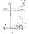
24:ゲート線終端
26:ゲート電極
40:半導体層
55、56:オーミックコンタクト層
62:データ線
65:ソース電極
66:ドレイン電極
68:データ線終端
74、76、78:コンタクトホール
82:画素電極
86:補助ゲート線終端
88:補助データ線終端
91、92、93、94、9124、9134、012、934、913、924:光遮断膜
Claims (30)
- ゲートラインと前記ゲートラインと交差するデータラインを含んで、
前記ゲートラインから絶縁基板上に形成されたゲート電極と、
前記ゲート電極上に絶縁されて形成された半導体層と、
前記ゲート電極と少なくとも一部分が重なって前記ゲート電極の周囲に配置された光遮断膜と、
前記データラインから形成されて前記半導体層と少なくとも一部分が重なるソース電極と、
前記ゲート電極を中心にして前記ソース電極と対向して前記半導体層と少なくとも一部分が重なるドレイン電極とを含むトランジスタ構造と、
前記トランジスタ構造上に絶縁されて前記ドレイン電極と電気的に接続された画素電極とを含むことを特徴とする薄膜トランジスタ基板。 - 前記光遮断膜は前記半導体層と同じ層に位置することを特徴とする請求項1に記載の薄膜トランジスタ基板。
- 前記光遮断膜は前記半導体層と実質的に同じ物質を含むことを特徴とする請求項2に記載の薄膜トランジスタ基板。
- 前記光遮断膜は光吸収物質を含むことを特徴とする請求項1に記載の薄膜トランジスタ基板。
- 前記光遮断膜はアモルファスシリコンを含むことを特徴とする請求項4に記載の薄膜トランジスタ基板。
- 前記光遮断膜は前記ソース電極及び前記ドレイン電極のうちいずれかの電極とも重ならないことを特徴とする請求項1に記載の薄膜トランジスタ基板。
- 前記光遮断膜は前記ソース電極及び前記ドレイン電極のうちいずれか一つの電極とのみ重なることを特徴とする請求項1に記載の薄膜トランジスタ基板。
- 前記半導体層は前記ゲート電極と完全に重なることを特徴とする請求項1に記載の薄膜トランジスタ基板。
- 前記光遮断膜は複数のサブ光遮断膜を含み、前記複数のサブ光遮断膜それぞれは相互に離隔されたことを特徴とする請求項1に記載の薄膜トランジスタ基板。
- 前記ゲート電極と前記光遮断膜が重なる幅が約3μm以下であることを特徴とする請求項1に記載の薄膜トランジスタ基板。
- 前記光遮断膜は約10μm以下の幅を有することを特徴とする請求項1に記載の薄膜トランジスタ基板。
- 絶縁基板上に形成されたゲート電極と前記ゲート電極と完全に重なって前記ゲート電極上に絶縁されて形成された半導体層と前記半導体層と同じ層に位置して前記ゲート電極と少なくとも一部分が重なって前記ゲート電極の周囲に配置された光遮断膜と前記半導体層と少なくとも一部分が重なるソース電極と前記ゲート電極を中心にして前記ソース電極と対向して前記半導体層と少なくとも一部分が重なるドレイン電極を含むトランジスタ構造と、前記トランジスタ構造上に絶縁されて前記ドレイン電極と電気的に接続された画素電極をと含む薄膜トランジスタ基板と、及び
前記薄膜トランジスタ基板と対向して、色フィルター及び共通電極を含むカラーフィルター基板とを含むことを特徴とする液晶表示装置。 - 前記光遮断膜は前記半導体層と同じ物質を含むことを特徴とする請求項12に記載の液晶表示装置。
- 前記光遮断膜は光吸収物質を含むことを特徴とする請求項12に記載の液晶表示装置。
- 前記光遮断膜はアモルファスシリコンを含むことを特徴とする請求項14に記載の液晶表示装置。
- 前記光遮断膜は前記ソース電極及び前記ドレイン電極のうちいずれか電極とも重ならないことを特徴とする請求項12に記載の液晶表示装置。
- 前記光遮断膜は前記ソース電極及び前記ドレイン電極のうちいずれか一つの電極とのみ重なることを特徴とする請求項12に記載の液晶表示装置。
- 前記光遮断膜は複数のサブ光遮断膜を含み、前記複数のサブ光遮断膜それぞれは相互に離隔されたことを特徴とする請求項12に記載の液晶表示装置。
- 前記ゲート電極と前記光遮断膜が重なる幅が約3μm以下であることを特徴とする請求項12に記載の液晶表示装置。
- 前記光遮断膜は約10μm以下の幅を有することを特徴とする請求項12に記載の液晶表示装置。
- 絶縁基板上にゲート電極を有するゲート線を形成し、
前記ゲート電極上に前記ゲート電極と絶縁された半導体層を形成し、
前記ゲート電極と少なくとも一部分が重なって前記ゲート電極の周囲に配置された光遮断膜を形成し、
前記ゲート線と交差して前記半導体層と少なくとも一部分が重なるソース電極を有するデータ線を形成し、
前記ゲート電極を中心にして前記ソース電極と対向して前記半導体層と少なくとも一部分が重なるドレイン電極を形成して、前記ゲート電極、前記半導体層、前記光遮断膜、前記ソース電極及び前記ドレイン電極からトランジスタ構造を形成し、
前記トランジスタ構造上に絶縁されて前記ドレイン電極と電気的に接続された画素電極を形成することを特徴とする薄膜トランジスタ基板の製造方法。 - 前記光遮断膜は前記半導体層と実質的に同じ物質を含むことを特徴とする請求項21に記載の薄膜トランジスタ基板の製造方法。
- 前記光遮断膜は光吸収物質を含むことを特徴とする請求項21に記載の薄膜トランジスタ基板の製造方法。
- 前記光遮断膜はアモルファスシリコンを含むことを特徴とする請求項23に記載の薄膜トランジスタ基板の製造方法。
- 前記光遮断膜は前記ソース電極及び前記ドレイン電極のうちいずれか電極とも重ならないことを特徴とする請求項21に記載の薄膜トランジスタ基板の製造方法。
- 前記光遮断膜は前記ソース電極及び前記ドレイン電極のうちいずれか一つの電極とのみ重なることを特徴とする請求項21に記載の薄膜トランジスタ基板の製造方法。
- 前記半導体層は前記ゲート電極と完全に重なることを特徴とする請求項21に記載の薄膜トランジスタ基板の製造方法。
- 前記光遮断膜は複数のサブ光遮断膜を含み、前記複数のサブ光遮断膜それぞれは相互に離隔されたことを特徴とする請求項21に記載の薄膜トランジスタ基板の製造方法。
- 前記ゲート電極と前記光遮断膜が重なる幅が約3μm以下であることを特徴とする請求項21に記載の薄膜トランジスタ基板の製造方法。
- 前記光遮断膜は約10μm以下の幅を有することを特徴とする請求項21に記載の薄膜トランジスタ基板の製造方法。
Applications Claiming Priority (1)
| Application Number | Priority Date | Filing Date | Title |
|---|---|---|---|
| KR1020050036798A KR101216688B1 (ko) | 2005-05-02 | 2005-05-02 | 박막 트랜지스터 기판 및 이를 포함하는 액정 표시 장치 |
Publications (2)
| Publication Number | Publication Date |
|---|---|
| JP2006313906A true JP2006313906A (ja) | 2006-11-16 |
| JP2006313906A5 JP2006313906A5 (ja) | 2009-06-18 |
Family
ID=37233587
Family Applications (1)
| Application Number | Title | Priority Date | Filing Date |
|---|---|---|---|
| JP2006126558A Pending JP2006313906A (ja) | 2005-05-02 | 2006-04-28 | 薄膜トランジスタ基板、これを含む液晶表示装置及び薄膜トランジスタ基板の製造方法 |
Country Status (5)
| Country | Link |
|---|---|
| US (1) | US7646023B2 (ja) |
| JP (1) | JP2006313906A (ja) |
| KR (1) | KR101216688B1 (ja) |
| CN (1) | CN1858911B (ja) |
| TW (1) | TWI420669B (ja) |
Cited By (8)
| Publication number | Priority date | Publication date | Assignee | Title |
|---|---|---|---|---|
| JP2009049058A (ja) * | 2007-08-14 | 2009-03-05 | Hitachi Displays Ltd | 半導体装置および表示装置 |
| JP2010206154A (ja) * | 2009-02-09 | 2010-09-16 | Hitachi Displays Ltd | 表示装置 |
| JP2016048706A (ja) * | 2014-08-27 | 2016-04-07 | 三菱電機株式会社 | アレイ基板およびその製造方法 |
| JP2016195283A (ja) * | 2016-08-08 | 2016-11-17 | 株式会社ジャパンディスプレイ | 表示装置及びその製造方法 |
| WO2017018203A1 (ja) * | 2015-07-24 | 2017-02-02 | ソニー株式会社 | 表示装置および撮像装置 |
| KR20180025521A (ko) * | 2016-08-31 | 2018-03-09 | 엘지디스플레이 주식회사 | 액정 표시장치 |
| US10914995B2 (en) | 2017-11-29 | 2021-02-09 | Panasonic Liquid Crystal Display Co., Ltd. | Liquid crystal display panel |
| JP7375238B2 (ja) | 2019-02-14 | 2023-11-07 | 株式会社ジャパンディスプレイ | 表示装置 |
Families Citing this family (31)
| Publication number | Priority date | Publication date | Assignee | Title |
|---|---|---|---|---|
| JP5303119B2 (ja) * | 2007-06-05 | 2013-10-02 | 株式会社ジャパンディスプレイ | 半導体装置 |
| US7738050B2 (en) * | 2007-07-06 | 2010-06-15 | Semiconductor Energy Laboratory Co., Ltd | Liquid crystal display device |
| TWI575293B (zh) * | 2007-07-20 | 2017-03-21 | 半導體能源研究所股份有限公司 | 液晶顯示裝置 |
| KR101499229B1 (ko) | 2008-04-07 | 2015-03-05 | 삼성디스플레이 주식회사 | 색필터를 포함하는 표시 장치 |
| KR101536194B1 (ko) * | 2008-05-19 | 2015-07-13 | 삼성디스플레이 주식회사 | 액정 표시 장치와 그 구동 방법 |
| KR101999970B1 (ko) | 2008-09-19 | 2019-07-15 | 가부시키가이샤 한도오따이 에네루기 켄큐쇼 | 반도체 장치 |
| TWI616707B (zh) | 2008-11-28 | 2018-03-01 | 半導體能源研究所股份有限公司 | 液晶顯示裝置 |
| JP2010156960A (ja) | 2008-12-03 | 2010-07-15 | Semiconductor Energy Lab Co Ltd | 液晶表示装置 |
| KR101719350B1 (ko) * | 2008-12-25 | 2017-03-23 | 가부시키가이샤 한도오따이 에네루기 켄큐쇼 | 반도체 장치 및 그 제작 방법 |
| KR101100959B1 (ko) * | 2010-03-10 | 2011-12-29 | 삼성모바일디스플레이주식회사 | 박막 트랜지스터, 그의 제조 방법 및 박막 트랜지스터를 구비하는 표시 장치 |
| TWI464508B (zh) * | 2010-11-22 | 2014-12-11 | Au Optronics Corp | 畫素陣列基板以及顯示面板 |
| US9568794B2 (en) * | 2010-12-20 | 2017-02-14 | Semiconductor Energy Laboratory Co., Ltd. | Display device |
| KR20130092848A (ko) * | 2012-02-13 | 2013-08-21 | 삼성전자주식회사 | 박막 트랜지스터 및 이를 채용한 디스플레이 패널 |
| KR101923717B1 (ko) * | 2012-05-24 | 2018-11-30 | 엘지디스플레이 주식회사 | 액정표시장치 어레이 기판 및 그 제조방법 |
| KR102276146B1 (ko) | 2013-09-10 | 2021-07-13 | 삼성디스플레이 주식회사 | 박막 트랜지스터 기판 및 이의 제조 방법 |
| KR102254619B1 (ko) | 2013-11-15 | 2021-05-24 | 삼성디스플레이 주식회사 | 표시 기판 및 그의 제조 방법 |
| KR101682079B1 (ko) * | 2013-12-30 | 2016-12-05 | 삼성디스플레이 주식회사 | 표시 장치 및 그 제조 방법 |
| CN104979364B (zh) * | 2014-04-01 | 2018-11-13 | 鸿富锦精密工业(深圳)有限公司 | 显示阵列基板及显示阵列基板的制造方法 |
| TWI582967B (zh) | 2014-04-01 | 2017-05-11 | 鴻海精密工業股份有限公司 | 顯示陣列基板及顯示陣列基板的製造方法 |
| TWI686899B (zh) * | 2014-05-02 | 2020-03-01 | 日商半導體能源研究所股份有限公司 | 半導體裝置、觸控感測器、顯示裝置 |
| CN114185216A (zh) | 2015-02-12 | 2022-03-15 | 株式会社半导体能源研究所 | 显示装置 |
| CN104716197B (zh) * | 2015-03-25 | 2019-06-07 | 京东方科技集团股份有限公司 | 一种氧化物薄膜晶体管及制作方法和阵列基板、显示装置 |
| KR102322015B1 (ko) * | 2015-04-07 | 2021-11-05 | 삼성디스플레이 주식회사 | 박막트랜지스터 어레이 기판의 제조 방법 및 그에 따라 제조된 박막 트랜지스터 어레이 기판 |
| TWI576646B (zh) | 2015-04-30 | 2017-04-01 | 群創光電股份有限公司 | 顯示裝置 |
| CN104992948B (zh) * | 2015-06-03 | 2018-07-06 | 京东方科技集团股份有限公司 | 一种薄膜晶体管、阵列基板及其制作方法 |
| CN105470268A (zh) | 2016-01-11 | 2016-04-06 | 京东方科技集团股份有限公司 | 一种阵列基板及其制作方法、显示装置 |
| CN106449656A (zh) * | 2016-10-26 | 2017-02-22 | 京东方科技集团股份有限公司 | 阵列基板及其制作方法、显示面板和显示装置 |
| KR102263122B1 (ko) * | 2017-10-19 | 2021-06-09 | 삼성디스플레이 주식회사 | 트랜지스터 표시판 |
| US11113095B2 (en) | 2019-04-30 | 2021-09-07 | Automation Anywhere, Inc. | Robotic process automation system with separate platform, bot and command class loaders |
| KR20210100795A (ko) * | 2020-02-06 | 2021-08-18 | 삼성디스플레이 주식회사 | 표시 장치 |
| JP2022150881A (ja) * | 2021-03-26 | 2022-10-07 | 株式会社ジャパンディスプレイ | 表示装置 |
Citations (3)
| Publication number | Priority date | Publication date | Assignee | Title |
|---|---|---|---|---|
| JPS6452129A (en) * | 1987-08-24 | 1989-02-28 | Toshiba Corp | Thin film transistor |
| JPH0449674A (ja) * | 1990-06-19 | 1992-02-19 | Nec Corp | 薄膜トランジスタ |
| JP2002141509A (ja) * | 2000-11-01 | 2002-05-17 | Matsushita Electric Ind Co Ltd | 薄膜トランジスタ及び液晶表示装置 |
Family Cites Families (9)
| Publication number | Priority date | Publication date | Assignee | Title |
|---|---|---|---|---|
| JP3264995B2 (ja) * | 1991-09-26 | 2002-03-11 | 株式会社東芝 | 液晶表示装置 |
| JPH09329808A (ja) | 1996-06-13 | 1997-12-22 | Toshiba Corp | 液晶表示装置 |
| JP2000122093A (ja) | 1998-10-20 | 2000-04-28 | Sharp Corp | 反射型液晶表示装置 |
| KR100309209B1 (ko) * | 1999-07-31 | 2001-09-29 | 구본준, 론 위라하디락사 | 액정 표시장치 제조방법 및 그 제조방법에 따른 액정표시장치 |
| JP2002250913A (ja) | 2001-02-27 | 2002-09-06 | Matsushita Electric Ind Co Ltd | 液晶表示装置とその製造方法 |
| KR100820647B1 (ko) * | 2001-10-29 | 2008-04-08 | 엘지.필립스 엘시디 주식회사 | 반투과 액정 표시 장치용 어레이기판 및 이의 제조방법 |
| TWI261135B (en) * | 2002-05-28 | 2006-09-01 | Chi Mei Optoelectronics Corp | Method for fabricating thin film transistors of a TFT-LCD |
| US7372528B2 (en) * | 2003-06-09 | 2008-05-13 | Samsung Electronics Co., Ltd. | Array substrate, method of manufacturing the same and liquid crystal display apparatus having the same |
| CN100504553C (zh) * | 2004-02-06 | 2009-06-24 | 三星电子株式会社 | 薄膜晶体管阵列面板及包括该薄膜晶体管阵列面板的液晶显示器 |
-
2005
- 2005-05-02 KR KR1020050036798A patent/KR101216688B1/ko active IP Right Grant
-
2006
- 2006-04-26 TW TW095114885A patent/TWI420669B/zh active
- 2006-04-28 JP JP2006126558A patent/JP2006313906A/ja active Pending
- 2006-04-29 CN CN2006100794529A patent/CN1858911B/zh active Active
- 2006-05-02 US US11/416,934 patent/US7646023B2/en not_active Expired - Fee Related
Patent Citations (3)
| Publication number | Priority date | Publication date | Assignee | Title |
|---|---|---|---|---|
| JPS6452129A (en) * | 1987-08-24 | 1989-02-28 | Toshiba Corp | Thin film transistor |
| JPH0449674A (ja) * | 1990-06-19 | 1992-02-19 | Nec Corp | 薄膜トランジスタ |
| JP2002141509A (ja) * | 2000-11-01 | 2002-05-17 | Matsushita Electric Ind Co Ltd | 薄膜トランジスタ及び液晶表示装置 |
Cited By (9)
| Publication number | Priority date | Publication date | Assignee | Title |
|---|---|---|---|---|
| JP2009049058A (ja) * | 2007-08-14 | 2009-03-05 | Hitachi Displays Ltd | 半導体装置および表示装置 |
| JP2010206154A (ja) * | 2009-02-09 | 2010-09-16 | Hitachi Displays Ltd | 表示装置 |
| JP2016048706A (ja) * | 2014-08-27 | 2016-04-07 | 三菱電機株式会社 | アレイ基板およびその製造方法 |
| WO2017018203A1 (ja) * | 2015-07-24 | 2017-02-02 | ソニー株式会社 | 表示装置および撮像装置 |
| JP2016195283A (ja) * | 2016-08-08 | 2016-11-17 | 株式会社ジャパンディスプレイ | 表示装置及びその製造方法 |
| KR20180025521A (ko) * | 2016-08-31 | 2018-03-09 | 엘지디스플레이 주식회사 | 액정 표시장치 |
| KR102621447B1 (ko) | 2016-08-31 | 2024-01-08 | 엘지디스플레이 주식회사 | 액정 표시장치 |
| US10914995B2 (en) | 2017-11-29 | 2021-02-09 | Panasonic Liquid Crystal Display Co., Ltd. | Liquid crystal display panel |
| JP7375238B2 (ja) | 2019-02-14 | 2023-11-07 | 株式会社ジャパンディスプレイ | 表示装置 |
Also Published As
| Publication number | Publication date |
|---|---|
| CN1858911B (zh) | 2012-05-30 |
| US7646023B2 (en) | 2010-01-12 |
| KR101216688B1 (ko) | 2012-12-31 |
| KR20060114744A (ko) | 2006-11-08 |
| TW200703660A (en) | 2007-01-16 |
| US20060243979A1 (en) | 2006-11-02 |
| CN1858911A (zh) | 2006-11-08 |
| TWI420669B (zh) | 2013-12-21 |
Similar Documents
| Publication | Publication Date | Title |
|---|---|---|
| KR101216688B1 (ko) | 박막 트랜지스터 기판 및 이를 포함하는 액정 표시 장치 | |
| JP5190625B2 (ja) | 液晶表示装置及びその不良画素修復方法 | |
| JP3307150B2 (ja) | アクティブマトリクス型表示装置 | |
| JP5317399B2 (ja) | 液晶表示装置 | |
| US20190227373A1 (en) | Liquid crystal display device and manufacturing method thereof | |
| US8324003B2 (en) | Method for manufacturing a thin film transistor array panel | |
| KR20040053636A (ko) | 박막 트랜지스터 어레이 기판 및 이를 포함하는 액정 표시장치 | |
| JP2001356372A (ja) | 液晶表示装置用薄膜トランジスタ基板及びその製造方法 | |
| KR20110060567A (ko) | 표시 장치, 박막 트랜지스터 기판 및 이의 제조 방법 | |
| KR20140047649A (ko) | 액정 표시 장치 | |
| JP2008046625A (ja) | 液晶表示装置 | |
| JP2004038186A (ja) | 半透過型液晶表示装置及びその製造方法 | |
| KR20100005457A (ko) | 박막 트랜지스터 표시판 및 이의 제조 방법 | |
| JP2009265662A (ja) | 高開口率アレイ基板、液晶表示装置およびこれらの製造方法 | |
| KR20160128518A (ko) | 표시장치 및 그 제조방법 | |
| KR102390430B1 (ko) | 액정 표시 장치 및 그의 제조 방법 | |
| KR20060090352A (ko) | 박막트랜지스터 기판과 그 제조방법 | |
| KR20080069798A (ko) | 액정 표시 장치 | |
| KR20070080107A (ko) | 빛샘 방지를 위한 액정 표시 장치 | |
| KR101012786B1 (ko) | 액정 표시 장치 | |
| KR20050019278A (ko) | 박막 트랜지스터 표시판 및 그의 제조 방법 | |
| KR20070018291A (ko) | 박막 트랜지스터 표시판 및 그의 제조 방법 | |
| KR20070008257A (ko) | 배선 및 그 형성 방법과 박막 트랜지스터 기판 및 그 제조방법 | |
| KR20050026300A (ko) | 박막 트랜지스터 표시판 및 이를 포함하는 표시 장치 | |
| KR20040000187A (ko) | 박막 트랜지스터 어레이 기판, 공통 전극 기판, 이들의제조 방법 및 이들을 포함하는 액정 표시 장치 |
Legal Events
| Date | Code | Title | Description |
|---|---|---|---|
| A521 | Written amendment |
Free format text: JAPANESE INTERMEDIATE CODE: A523 Effective date: 20090424 |
|
| A621 | Written request for application examination |
Free format text: JAPANESE INTERMEDIATE CODE: A621 Effective date: 20090424 |
|
| A977 | Report on retrieval |
Free format text: JAPANESE INTERMEDIATE CODE: A971007 Effective date: 20120518 |
|
| A131 | Notification of reasons for refusal |
Free format text: JAPANESE INTERMEDIATE CODE: A131 Effective date: 20120605 |
|
| A521 | Written amendment |
Free format text: JAPANESE INTERMEDIATE CODE: A523 Effective date: 20120904 |
|
| A02 | Decision of refusal |
Free format text: JAPANESE INTERMEDIATE CODE: A02 Effective date: 20121002 |
|
| A711 | Notification of change in applicant |
Free format text: JAPANESE INTERMEDIATE CODE: A712 Effective date: 20121213 |