JP2005328272A - Pll回路およびそれを用いた周波数設定回路 - Google Patents
Pll回路およびそれを用いた周波数設定回路 Download PDFInfo
- Publication number
- JP2005328272A JP2005328272A JP2004143752A JP2004143752A JP2005328272A JP 2005328272 A JP2005328272 A JP 2005328272A JP 2004143752 A JP2004143752 A JP 2004143752A JP 2004143752 A JP2004143752 A JP 2004143752A JP 2005328272 A JP2005328272 A JP 2005328272A
- Authority
- JP
- Japan
- Prior art keywords
- phase
- voltage
- filter
- signal
- phase shifter
- Prior art date
- Legal status (The legal status is an assumption and is not a legal conclusion. Google has not performed a legal analysis and makes no representation as to the accuracy of the status listed.)
- Pending
Links
- 239000003990 capacitor Substances 0.000 claims abstract description 47
- 238000006243 chemical reaction Methods 0.000 claims 1
- 238000009499 grossing Methods 0.000 claims 1
- 238000004519 manufacturing process Methods 0.000 abstract description 17
- 230000003071 parasitic effect Effects 0.000 description 22
- 238000000034 method Methods 0.000 description 18
- 101100462367 Aspergillus niger (strain CBS 513.88 / FGSC A1513) otaB gene Proteins 0.000 description 14
- 101100462369 Aspergillus niger (strain CBS 513.88 / FGSC A1513) otaC gene Proteins 0.000 description 13
- 101100462365 Aspergillus niger (strain CBS 513.88 / FGSC A1513) otaA gene Proteins 0.000 description 12
- 101100462371 Aspergillus niger (strain CBS 513.88 / FGSC A1513) otaD gene Proteins 0.000 description 8
- 238000003780 insertion Methods 0.000 description 8
- 230000037431 insertion Effects 0.000 description 8
- 101100462373 Aspergillus niger (strain CBS 513.88 / FGSC A1513) otaR1 gene Proteins 0.000 description 7
- 238000010586 diagram Methods 0.000 description 7
- 230000000694 effects Effects 0.000 description 7
- 238000012546 transfer Methods 0.000 description 7
- 230000008859 change Effects 0.000 description 6
- 230000007850 degeneration Effects 0.000 description 6
- 230000003111 delayed effect Effects 0.000 description 6
- RDYMFSUJUZBWLH-UHFFFAOYSA-N endosulfan Chemical compound C12COS(=O)OCC2C2(Cl)C(Cl)=C(Cl)C1(Cl)C2(Cl)Cl RDYMFSUJUZBWLH-UHFFFAOYSA-N 0.000 description 4
- 238000012986 modification Methods 0.000 description 3
- 230000004048 modification Effects 0.000 description 3
- 238000013459 approach Methods 0.000 description 2
- 238000001514 detection method Methods 0.000 description 2
- 230000035945 sensitivity Effects 0.000 description 2
- 101100439975 Arabidopsis thaliana CLPF gene Proteins 0.000 description 1
- 230000002238 attenuated effect Effects 0.000 description 1
- 230000008901 benefit Effects 0.000 description 1
- 239000002131 composite material Substances 0.000 description 1
- 238000007796 conventional method Methods 0.000 description 1
- 230000007423 decrease Effects 0.000 description 1
- 238000013461 design Methods 0.000 description 1
- 230000006866 deterioration Effects 0.000 description 1
- 230000010355 oscillation Effects 0.000 description 1
- 230000008569 process Effects 0.000 description 1
- 230000004044 response Effects 0.000 description 1
- 239000004065 semiconductor Substances 0.000 description 1
Images


Classifications
-
- H—ELECTRICITY
- H03—ELECTRONIC CIRCUITRY
- H03L—AUTOMATIC CONTROL, STARTING, SYNCHRONISATION, OR STABILISATION OF GENERATORS OF ELECTRONIC OSCILLATIONS OR PULSES
- H03L7/00—Automatic control of frequency or phase; Synchronisation
- H03L7/06—Automatic control of frequency or phase; Synchronisation using a reference signal applied to a frequency- or phase-locked loop
- H03L7/08—Details of the phase-locked loop
- H03L7/081—Details of the phase-locked loop provided with an additional controlled phase shifter
- H03L7/0812—Details of the phase-locked loop provided with an additional controlled phase shifter and where no voltage or current controlled oscillator is used
-
- H—ELECTRICITY
- H03—ELECTRONIC CIRCUITRY
- H03H—IMPEDANCE NETWORKS, e.g. RESONANT CIRCUITS; RESONATORS
- H03H11/00—Networks using active elements
- H03H11/02—Multiple-port networks
- H03H11/04—Frequency selective two-port networks
- H03H11/0422—Frequency selective two-port networks using transconductance amplifiers, e.g. gmC filters
-
- H—ELECTRICITY
- H03—ELECTRONIC CIRCUITRY
- H03H—IMPEDANCE NETWORKS, e.g. RESONANT CIRCUITS; RESONATORS
- H03H11/00—Networks using active elements
- H03H11/02—Multiple-port networks
- H03H11/04—Frequency selective two-port networks
- H03H11/12—Frequency selective two-port networks using amplifiers with feedback
- H03H11/1291—Current or voltage controlled filters
-
- H—ELECTRICITY
- H03—ELECTRONIC CIRCUITRY
- H03L—AUTOMATIC CONTROL, STARTING, SYNCHRONISATION, OR STABILISATION OF GENERATORS OF ELECTRONIC OSCILLATIONS OR PULSES
- H03L7/00—Automatic control of frequency or phase; Synchronisation
- H03L7/06—Automatic control of frequency or phase; Synchronisation using a reference signal applied to a frequency- or phase-locked loop
- H03L7/08—Details of the phase-locked loop
- H03L7/0805—Details of the phase-locked loop the loop being adapted to provide an additional control signal for use outside the loop
-
- H—ELECTRICITY
- H03—ELECTRONIC CIRCUITRY
- H03L—AUTOMATIC CONTROL, STARTING, SYNCHRONISATION, OR STABILISATION OF GENERATORS OF ELECTRONIC OSCILLATIONS OR PULSES
- H03L7/00—Automatic control of frequency or phase; Synchronisation
- H03L7/06—Automatic control of frequency or phase; Synchronisation using a reference signal applied to a frequency- or phase-locked loop
- H03L7/08—Details of the phase-locked loop
- H03L7/085—Details of the phase-locked loop concerning mainly the frequency- or phase-detection arrangement including the filtering or amplification of its output signal
-
- H—ELECTRICITY
- H03—ELECTRONIC CIRCUITRY
- H03J—TUNING RESONANT CIRCUITS; SELECTING RESONANT CIRCUITS
- H03J2200/00—Indexing scheme relating to tuning resonant circuits and selecting resonant circuits
- H03J2200/18—Tuning of a master filter in order to tune its slave filter
Abstract
位相器として用いる2次gm−Cフィルタの位相量がトランジスタの製造バラツキや温度特性、容量値の製造バラツキがあっても一定値となることで2次gm−Cフィルタのカットオフ周波数を一定周波数に設定するPLL回路と、同一の制御信号で制御することでgm−Cフィルタのカットオフ周波数もトランジスタの製造バラツキや温度特性、容量値の製造バラツキがあっても一定となる周波数設定回路の提供。
【解決手段】
所定の周波数の交流信号が複数個のOTAと容量から構成される位相器101に入力され、前記位相器101への入力信号と前記位相器101からの出力信号を入力とする位相比較器105が入力信号間の位相差に応じた信号を出力し、前記位相器の出力信号の直流電圧を増幅する増幅器108を介して出力電圧を制御信号として、前記位相器を構成する少なくとも1つのOTAのトランスコンダクタンス(gm)を変化させることで前記位相器での位相差が一定値になるように制御するフェーズロックドループ(PLL)を持つ。
【選択図】
図1
Description

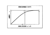
と表わされる。ここで、ω0 2は極の周波数であり、Qは極のQ値である。
となる。
である。
となる。
と表わされ、良く知られた時定数の式が得られる。
となる。
と表わされる。
VLPF<VDD/4−VDD/(2GV)
となり、差動増幅器108の出力電圧VCONは、GND電圧に張り付いている。したがって、デジェネレーション抵抗値は、無限大となり、gm値は最小値(=0)となり、位相器101の出力も固定となる。すなわち、位相検出器の出力は、周波数fREFの交流信号がそのままデューティ50%の矩形波となる。
となる。
と表わされる。
となる。
と表わされる。
となる。
と表わされる。
(i) LCRラダー手法
(ii) バイクァッド(biquad)手法
の2つの手法が知られている。
(i) LCRラダーフィルタをエミュレートする手法
(ii) バイクァッド手法
がある。
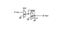
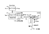
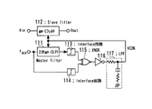
102 gm−Cフィルタ(スレーブフィルタ)
103、104 インタフェース回路
105 XNOR回路
106 インバータ
107 ループフィルタ
108 増幅器
109 スイッチ
110 V−I変換器
111 2次gm−Cフィルタ(マスタフィルタ)
112 gm−Cフィルタ(スレーブフィルタ)
113、114 インタフェース回路
115 XNOR回路
116 インバータ
117 ループフィルタ
Claims (13)
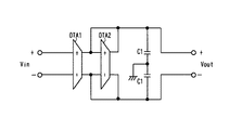
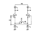
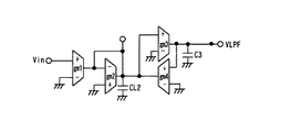
- 所定の周波数の交流信号を入力信号として入力し、複数のトランスコンダクタンスアンプ(「OTA」という)と容量から構成され、前記入力信号を所定の位相だけ可変させた信号を出力する位相器と、
前記位相器への前記入力信号と前記位相器からの出力信号とを入力とし、入力した信号間の位相差に応じた信号を出力する位相比較器と、
前記位相比較器の出力信号の直流電圧を増幅する増幅器と、
を備え、
前記増幅器の出力電圧を制御信号として、前記位相器を構成する少なくとも1つのOTAのトランスコンダクタンス(gm)を変化させることで、前記位相器での位相差が一定値になるように制御されるフェーズロックドループ(PLL)を有する、ことを特徴とするPLL回路。 - 所定の周波数の交流信号を入力信号として入力し、複数のトランスコンダクタンスアンプ(「OTA」という)と容量から構成され、前記入力信号を所定の位相だけ可変させた信号を出力する位相器と、
前記位相器への前記入力信号と前記位相器からの出力信号とを入力とし、入力した信号間の位相差に応じた信号を出力する位相比較器と、
前記位相比較器の出力信号の直流電圧を増幅する増幅器と、
前記増幅器の出力電圧を電流に変換する電圧−電流変換器と、
を備え、
前記電圧-電流変換器の出力電流を制御信号として、前記位相器を構成する少なくとも1つのOTAのトランスコンダクタンス(gm)を変化させることで、前記位相器での位相差が一定値になるように制御するフェーズロックドループ(PLL)を有する、ことを特徴とするPLL回路。 - 前記位相器が、奇数次のフィルタからなる、ことを特徴とする請求項1又は2記載のPLL回路。
- 前記増幅器が、前記直流電圧と入力された基準電圧とを差動増幅する差動増幅器よりなる、ことを特徴とする請求項3記載のPLL回路。
- 前記基準電圧は電源電圧の半分以下の電圧に設定されている、ことを特徴とする請求項4記載のPLL回路。
- 前記基準電圧は、前記電源電圧の1/4に設定される、ことを特徴とする請求項5記載のPLL回路。
- 前記位相比較器の出力を平滑化するフィルタを前記差動増幅器に一体に備えてなる、ことを特徴とする請求項4記載のPLL回路。
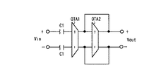
- 複数のトランスコンダクタンスアンプ(「OTA」という)と容量から構成される奇数次のフィルタよりなり、所定の周波数の交流信号を入力信号として入力し前記入力信号を所定位相シフトした信号を出力する位相器と、
前記位相器への前記入力信号と、前記位相器から出力される信号とを入力とし、入力した信号間の位相差に応じた信号を出力する位相比較器と、
前記位相比較器の出力信号を受け直流電圧を出力するループフィルタと、
前記ループフィルタの出力電圧と、入力される基準電圧とを差動増幅する差動増幅器と、
を備え、
前記差動増幅器の出力電圧、又は前記出力電圧を電圧−電流変換回路で電流に変換した信号を、制御信号として前記位相器に帰還入力し、前記制御信号により、前記位相器を構成する少なくとも1つのOTAのトランスコンダクタンス(gm)を可変させ前記位相器での位相差が一定値になるように制御するフェーズロックドループ(PLL)を有し、
前記基準電圧は、電源電圧の半分以下とされる、ことを特徴とするPLL回路。 - 前記位相器は位相を45度シフトし、前記基準電圧は電源電圧の1/4とされる、ことを特徴とする請求項8記載のPLL回路。
- 前記位相比較器の出力信号を受け前記直流電圧を出力するループフィルタを構成する少なくとも1つの容量を充電する充電手段を有し、
前記充電手段により、前記容量が前記基準電圧とほぼ等しい電圧に充電される、ことを特徴とする請求項4乃至9のいずれか一に記載のPLL回路。 - 前記充電手段が、前記ループフィルタを構成する少なくとも1つの容量と前記基準電圧との接続をオン・オフ制御するスイッチ回路を含む、ことを特徴とする請求項10記載のPLL回路。
- 請求項1乃至11のいずれか一に記載のPLL回路を備え、
OTAと容量より構成され、前記PLL回路からの前記制御信号により、前記位相器と共通に制御されるOTAを有するフィルタ(「gm−Cフィルタ」という)を備えている、ことを特徴とする周波数設定回路。 - 前記位相器の容量値は、前記gm−Cフィルタに用いる容量値とほぼ同じ値に合わされる、ことを特徴とする請求項12に記載の周波数設定回路。
Priority Applications (3)
| Application Number | Priority Date | Filing Date | Title |
|---|---|---|---|
| JP2004143752A JP2005328272A (ja) | 2004-05-13 | 2004-05-13 | Pll回路およびそれを用いた周波数設定回路 |
| US11/126,294 US7443214B2 (en) | 2004-05-13 | 2005-05-11 | PLL circuit and frequency setting circuit using the same |
| GB0509851A GB2415102B (en) | 2004-05-13 | 2005-05-13 | PLL circuit and frequency-setting circuit using the same |
Applications Claiming Priority (1)
| Application Number | Priority Date | Filing Date | Title |
|---|---|---|---|
| JP2004143752A JP2005328272A (ja) | 2004-05-13 | 2004-05-13 | Pll回路およびそれを用いた周波数設定回路 |
Publications (2)
| Publication Number | Publication Date |
|---|---|
| JP2005328272A true JP2005328272A (ja) | 2005-11-24 |
| JP2005328272A5 JP2005328272A5 (ja) | 2007-03-01 |
Family
ID=34709189
Family Applications (1)
| Application Number | Title | Priority Date | Filing Date |
|---|---|---|---|
| JP2004143752A Pending JP2005328272A (ja) | 2004-05-13 | 2004-05-13 | Pll回路およびそれを用いた周波数設定回路 |
Country Status (3)
| Country | Link |
|---|---|
| US (1) | US7443214B2 (ja) |
| JP (1) | JP2005328272A (ja) |
| GB (1) | GB2415102B (ja) |
Cited By (3)
| Publication number | Priority date | Publication date | Assignee | Title |
|---|---|---|---|---|
| JP2007166054A (ja) * | 2005-12-12 | 2007-06-28 | Niigata Seimitsu Kk | フィルタの自動調整装置 |
| WO2014122753A1 (ja) * | 2013-02-07 | 2014-08-14 | マークデバイシス株式会社 | フローティングイミタンス形成回路及びこれを用いたフローティングイミタンス回路 |
| JP2019071527A (ja) * | 2017-10-06 | 2019-05-09 | ザインエレクトロニクス株式会社 | 増幅回路 |
Families Citing this family (11)
| Publication number | Priority date | Publication date | Assignee | Title |
|---|---|---|---|---|
| EP1806842B1 (fr) * | 2005-12-30 | 2009-09-02 | Stmicroelectronics SA | Circuit de filtrage à transconductance, en particulier pour un téléphone cellulaire |
| JP2008078995A (ja) * | 2006-09-21 | 2008-04-03 | Nec Electronics Corp | 移相回路 |
| CN103048922B (zh) * | 2011-10-13 | 2015-08-12 | 中国科学院电子学研究所 | 基于跨导-电容结构的模拟比例积分控制器电路 |
| US8674736B2 (en) * | 2012-07-31 | 2014-03-18 | Fujitsu Limited | Clock synchronization circuit |
| US10175271B2 (en) * | 2012-12-31 | 2019-01-08 | Silicon Laboratories Inc. | Apparatus for differencing comparator and associated methods |
| US8947125B2 (en) * | 2013-02-21 | 2015-02-03 | Qualcomm Incorporated | Fast, low power comparator with dynamic bias background |
| US8760203B1 (en) | 2013-05-01 | 2014-06-24 | Cypress Semiconductor Corporation | OTA based fast lock PLL |
| CN113328727A (zh) * | 2018-01-29 | 2021-08-31 | 三峡大学 | 一种宽带90°移相方法 |
| US11025256B2 (en) * | 2018-08-21 | 2021-06-01 | Mediatek Inc. | Filter with direct current level shift and associated phase-locked loop circuit |
| CN109167572A (zh) * | 2018-10-12 | 2019-01-08 | 南京屹信航天科技有限公司 | 一种用于小型化odu接收通道的频率合成器 |
| CN116830453A (zh) * | 2021-03-18 | 2023-09-29 | 华为技术有限公司 | 移相器、相控阵、电子设备和终端设备 |
Citations (6)
| Publication number | Priority date | Publication date | Assignee | Title |
|---|---|---|---|---|
| JPH02130026A (ja) * | 1988-11-09 | 1990-05-18 | Oki Electric Ind Co Ltd | フェーズロックループ回路 |
| JPH0356227U (ja) * | 1989-10-03 | 1991-05-30 | ||
| JPH07212185A (ja) * | 1994-01-12 | 1995-08-11 | Hitachi Ltd | アナログフィルタ回路 |
| JP2000209066A (ja) * | 1999-01-14 | 2000-07-28 | Mitsubishi Electric Corp | フィルタ調整装置 |
| JP2002084189A (ja) * | 2000-03-21 | 2002-03-22 | Ntt Electornics Corp | 位相同期回路 |
| JP2003264449A (ja) * | 2002-03-11 | 2003-09-19 | Asahi Kasei Microsystems Kk | Gm−Cフィルタ及びそのテスト方法 |
Family Cites Families (17)
| Publication number | Priority date | Publication date | Assignee | Title |
|---|---|---|---|---|
| US4628272A (en) * | 1984-10-01 | 1986-12-09 | Motorola, Inc. | Tuned inductorless active phase shift demodulator |
| JP2973491B2 (ja) | 1990-08-22 | 1999-11-08 | ソニー株式会社 | Ntsc/pal信号判別回路およびこの判別回路を用いたアクティブフィルタ |
| US5245565A (en) * | 1991-07-31 | 1993-09-14 | International Microelectronic Products | Digitally programmable linear phase filter having phase equalization |
| JP3180424B2 (ja) * | 1992-03-11 | 2001-06-25 | ソニー株式会社 | 出力制御回路 |
| US5606284A (en) * | 1994-08-26 | 1997-02-25 | Matsushita Electric Industrial Co., Ltd. | Automatic gain control device for producing constant amplitude output signal |
| JPH08191231A (ja) | 1995-01-06 | 1996-07-23 | Sony Corp | フィルタ回路 |
| GB2323985B (en) | 1997-03-07 | 2001-09-05 | Mitel Semiconductor Ltd | Frequency tracking arrangments |
| GB9704719D0 (en) * | 1997-03-07 | 1997-04-23 | Plessey Semiconductors Ltd | Frequency tracking arrangements |
| US6172569B1 (en) * | 1999-03-16 | 2001-01-09 | Analog Devices, Inc. | Transconductance filter control system |
| US6323692B1 (en) * | 2000-05-19 | 2001-11-27 | Advanced Micro Devices, Inc. | Transconductance compensation circuit having a phase detector circuit with cycle slipping recovery operation and method |
| JP2002076842A (ja) | 2000-08-30 | 2002-03-15 | Sony Corp | フィルタ装置、フィルタ制御方法、及び受信装置 |
| US6549074B2 (en) * | 2000-12-05 | 2003-04-15 | Nippon Telegraph And Telephone Corporation | Transconductance amplifier, filter using the transconductance amplifier and tuning circuitry for transconductance amplifier in the filter |
| JP3606373B2 (ja) * | 2000-12-26 | 2005-01-05 | シャープ株式会社 | フィルタ具備装置 |
| US7051063B2 (en) * | 2002-05-03 | 2006-05-23 | Atheros Communications, Inc. | Integrated low power channel select filter having high dynamic range and bandwidth |
| US6842710B1 (en) * | 2002-08-22 | 2005-01-11 | Cypress Semiconductor Corporation | Calibration of integrated circuit time constants |
| US6977542B2 (en) * | 2002-11-25 | 2005-12-20 | Texas Instruments Incorporated | Adjusting the trans-conductance of a filter |
| JP2004336152A (ja) * | 2003-04-30 | 2004-11-25 | Sony Corp | 正弦波発生回路 |
-
2004
- 2004-05-13 JP JP2004143752A patent/JP2005328272A/ja active Pending
-
2005
- 2005-05-11 US US11/126,294 patent/US7443214B2/en not_active Expired - Fee Related
- 2005-05-13 GB GB0509851A patent/GB2415102B/en not_active Expired - Fee Related
Patent Citations (6)
| Publication number | Priority date | Publication date | Assignee | Title |
|---|---|---|---|---|
| JPH02130026A (ja) * | 1988-11-09 | 1990-05-18 | Oki Electric Ind Co Ltd | フェーズロックループ回路 |
| JPH0356227U (ja) * | 1989-10-03 | 1991-05-30 | ||
| JPH07212185A (ja) * | 1994-01-12 | 1995-08-11 | Hitachi Ltd | アナログフィルタ回路 |
| JP2000209066A (ja) * | 1999-01-14 | 2000-07-28 | Mitsubishi Electric Corp | フィルタ調整装置 |
| JP2002084189A (ja) * | 2000-03-21 | 2002-03-22 | Ntt Electornics Corp | 位相同期回路 |
| JP2003264449A (ja) * | 2002-03-11 | 2003-09-19 | Asahi Kasei Microsystems Kk | Gm−Cフィルタ及びそのテスト方法 |
Cited By (7)
| Publication number | Priority date | Publication date | Assignee | Title |
|---|---|---|---|---|
| JP2007166054A (ja) * | 2005-12-12 | 2007-06-28 | Niigata Seimitsu Kk | フィルタの自動調整装置 |
| WO2014122753A1 (ja) * | 2013-02-07 | 2014-08-14 | マークデバイシス株式会社 | フローティングイミタンス形成回路及びこれを用いたフローティングイミタンス回路 |
| WO2014122808A1 (ja) * | 2013-02-07 | 2014-08-14 | マークデバイシス株式会社 | イミタンス変換回路及びフィルタ |
| US9401695B2 (en) | 2013-02-07 | 2016-07-26 | Marcdevices Co., Ltd. | Immittance conversion circuit and filter |
| JP6041907B2 (ja) * | 2013-02-07 | 2016-12-14 | マークデバイシス株式会社 | イミタンス変換回路及びフィルタ |
| JP2019071527A (ja) * | 2017-10-06 | 2019-05-09 | ザインエレクトロニクス株式会社 | 増幅回路 |
| JP7081783B2 (ja) | 2017-10-06 | 2022-06-07 | ザインエレクトロニクス株式会社 | 増幅回路 |
Also Published As
| Publication number | Publication date |
|---|---|
| US20050253633A1 (en) | 2005-11-17 |
| GB2415102B (en) | 2006-11-22 |
| GB2415102A (en) | 2005-12-14 |
| GB0509851D0 (en) | 2005-06-22 |
| US7443214B2 (en) | 2008-10-28 |
Similar Documents
| Publication | Publication Date | Title |
|---|---|---|
| US7443214B2 (en) | PLL circuit and frequency setting circuit using the same | |
| US7180364B2 (en) | Filter apparatus including slave gm-C filter with frequency characteristics automatically tuned by master circuit | |
| Gopinathan et al. | Design considerations for high-frequency continuous-time filters and implementation of an antialiasing filter for digital video | |
| Khorramabadi et al. | High-frequency CMOS continuous-time filters | |
| US11201625B2 (en) | Phase locked loop | |
| TWI448083B (zh) | 環振盪器中的延遲單元及相關方法 | |
| US6335655B1 (en) | Filter circuit | |
| US20050156661A1 (en) | Filter apparatus including differential slave gm-C filter with frequency characteristics automatically tuned by master circuit | |
| JP2006191373A (ja) | アナログフィルタ回路、およびその調整方法 | |
| EP3079255A1 (en) | Multipath feedforward band pass amplifier | |
| TWI684329B (zh) | 用於迴路電路之基於電壓調節器的迴路濾波器以及迴路濾波方法 | |
| EP1384324B1 (en) | A cmos circuit with constant output swing and variable time delay for a voltage controlled oscillator | |
| JP2008278016A (ja) | Pll回路及びそれを用いた周波数設定回路 | |
| US7248103B2 (en) | Complex band-pass filter | |
| US7642867B2 (en) | Simple technique for reduction of gain in a voltage controlled oscillator | |
| JP4598691B2 (ja) | Pll回路及び半導体装置 | |
| JP5078393B2 (ja) | フィルターの中心周波数を自動的に校正できる校正ループ、フィルター回路及び関連方法 | |
| JP4323384B2 (ja) | フィードバック制御回路 | |
| Mehrmanesh et al. | An ultra low-voltage Gm-C filter for video applications | |
| CN110113024B (zh) | 一种多相滤波电路 | |
| JP2010093361A (ja) | フィルタ回路 | |
| US10972075B2 (en) | Active quadrature circuits for high frequency applications | |
| Kasimis et al. | OTA based frequency tuning system with reduced effect of DC offsets | |
| JP3147102B2 (ja) | 遮断周波数制御回路 | |
| Kassimis et al. | OTA based frequency tuning system |
Legal Events
| Date | Code | Title | Description |
|---|---|---|---|
| A521 | Request for written amendment filed |
Free format text: JAPANESE INTERMEDIATE CODE: A523 Effective date: 20070115 |
|
| A621 | Written request for application examination |
Free format text: JAPANESE INTERMEDIATE CODE: A621 Effective date: 20070405 |
|
| A977 | Report on retrieval |
Free format text: JAPANESE INTERMEDIATE CODE: A971007 Effective date: 20081128 |
|
| A131 | Notification of reasons for refusal |
Free format text: JAPANESE INTERMEDIATE CODE: A131 Effective date: 20090224 |
|
| A521 | Request for written amendment filed |
Free format text: JAPANESE INTERMEDIATE CODE: A523 Effective date: 20090427 |
|
| A131 | Notification of reasons for refusal |
Free format text: JAPANESE INTERMEDIATE CODE: A131 Effective date: 20100615 |
|
| A02 | Decision of refusal |
Free format text: JAPANESE INTERMEDIATE CODE: A02 Effective date: 20101019 |