JP2005294828A - 集積回路構造及び形成方法(高移動度平面cmossoi) - Google Patents
集積回路構造及び形成方法(高移動度平面cmossoi) Download PDFInfo
- Publication number
- JP2005294828A JP2005294828A JP2005085789A JP2005085789A JP2005294828A JP 2005294828 A JP2005294828 A JP 2005294828A JP 2005085789 A JP2005085789 A JP 2005085789A JP 2005085789 A JP2005085789 A JP 2005085789A JP 2005294828 A JP2005294828 A JP 2005294828A
- Authority
- JP
- Japan
- Prior art keywords
- substrate
- forming
- opening
- insulating layer
- type
- Prior art date
- Legal status (The legal status is an assumption and is not a legal conclusion. Google has not performed a legal analysis and makes no representation as to the accuracy of the status listed.)
- Granted
Links
Images


Classifications
-
- H—ELECTRICITY
- H10—SEMICONDUCTOR DEVICES; ELECTRIC SOLID-STATE DEVICES NOT OTHERWISE PROVIDED FOR
- H10P—GENERIC PROCESSES OR APPARATUS FOR THE MANUFACTURE OR TREATMENT OF DEVICES COVERED BY CLASS H10
- H10P90/00—Preparation of wafers not covered by a single main group of this subclass, e.g. wafer reinforcement
- H10P90/19—Preparing inhomogeneous wafers
- H10P90/1904—Preparing vertically inhomogeneous wafers
- H10P90/1906—Preparing SOI wafers
- H10P90/1914—Preparing SOI wafers using bonding
-
- H—ELECTRICITY
- H10—SEMICONDUCTOR DEVICES; ELECTRIC SOLID-STATE DEVICES NOT OTHERWISE PROVIDED FOR
- H10D—INORGANIC ELECTRIC SEMICONDUCTOR DEVICES
- H10D30/00—Field-effect transistors [FET]
- H10D30/01—Manufacture or treatment
- H10D30/021—Manufacture or treatment of FETs having insulated gates [IGFET]
- H10D30/024—Manufacture or treatment of FETs having insulated gates [IGFET] of fin field-effect transistors [FinFET]
-
- H—ELECTRICITY
- H10—SEMICONDUCTOR DEVICES; ELECTRIC SOLID-STATE DEVICES NOT OTHERWISE PROVIDED FOR
- H10D—INORGANIC ELECTRIC SEMICONDUCTOR DEVICES
- H10D30/00—Field-effect transistors [FET]
- H10D30/60—Insulated-gate field-effect transistors [IGFET]
- H10D30/62—Fin field-effect transistors [FinFET]
-
- H—ELECTRICITY
- H10—SEMICONDUCTOR DEVICES; ELECTRIC SOLID-STATE DEVICES NOT OTHERWISE PROVIDED FOR
- H10D—INORGANIC ELECTRIC SEMICONDUCTOR DEVICES
- H10D84/00—Integrated devices formed in or on semiconductor substrates that comprise only semiconducting layers, e.g. on Si wafers or on GaAs-on-Si wafers
- H10D84/01—Manufacture or treatment
- H10D84/0123—Integrating together multiple components covered by H10D12/00 or H10D30/00, e.g. integrating multiple IGBTs
- H10D84/0126—Integrating together multiple components covered by H10D12/00 or H10D30/00, e.g. integrating multiple IGBTs the components including insulated gates, e.g. IGFETs
- H10D84/0165—Integrating together multiple components covered by H10D12/00 or H10D30/00, e.g. integrating multiple IGBTs the components including insulated gates, e.g. IGFETs the components including complementary IGFETs, e.g. CMOS devices
- H10D84/0167—Manufacturing their channels
-
- H—ELECTRICITY
- H10—SEMICONDUCTOR DEVICES; ELECTRIC SOLID-STATE DEVICES NOT OTHERWISE PROVIDED FOR
- H10D—INORGANIC ELECTRIC SEMICONDUCTOR DEVICES
- H10D84/00—Integrated devices formed in or on semiconductor substrates that comprise only semiconducting layers, e.g. on Si wafers or on GaAs-on-Si wafers
- H10D84/01—Manufacture or treatment
- H10D84/0123—Integrating together multiple components covered by H10D12/00 or H10D30/00, e.g. integrating multiple IGBTs
- H10D84/0126—Integrating together multiple components covered by H10D12/00 or H10D30/00, e.g. integrating multiple IGBTs the components including insulated gates, e.g. IGFETs
- H10D84/0165—Integrating together multiple components covered by H10D12/00 or H10D30/00, e.g. integrating multiple IGBTs the components including insulated gates, e.g. IGFETs the components including complementary IGFETs, e.g. CMOS devices
- H10D84/0188—Manufacturing their isolation regions
-
- H—ELECTRICITY
- H10—SEMICONDUCTOR DEVICES; ELECTRIC SOLID-STATE DEVICES NOT OTHERWISE PROVIDED FOR
- H10D—INORGANIC ELECTRIC SEMICONDUCTOR DEVICES
- H10D84/00—Integrated devices formed in or on semiconductor substrates that comprise only semiconducting layers, e.g. on Si wafers or on GaAs-on-Si wafers
- H10D84/01—Manufacture or treatment
- H10D84/0123—Integrating together multiple components covered by H10D12/00 or H10D30/00, e.g. integrating multiple IGBTs
- H10D84/0126—Integrating together multiple components covered by H10D12/00 or H10D30/00, e.g. integrating multiple IGBTs the components including insulated gates, e.g. IGFETs
- H10D84/0165—Integrating together multiple components covered by H10D12/00 or H10D30/00, e.g. integrating multiple IGBTs the components including insulated gates, e.g. IGFETs the components including complementary IGFETs, e.g. CMOS devices
- H10D84/0193—Integrating together multiple components covered by H10D12/00 or H10D30/00, e.g. integrating multiple IGBTs the components including insulated gates, e.g. IGFETs the components including complementary IGFETs, e.g. CMOS devices the components including FinFETs
-
- H—ELECTRICITY
- H10—SEMICONDUCTOR DEVICES; ELECTRIC SOLID-STATE DEVICES NOT OTHERWISE PROVIDED FOR
- H10D—INORGANIC ELECTRIC SEMICONDUCTOR DEVICES
- H10D84/00—Integrated devices formed in or on semiconductor substrates that comprise only semiconducting layers, e.g. on Si wafers or on GaAs-on-Si wafers
- H10D84/01—Manufacture or treatment
- H10D84/02—Manufacture or treatment characterised by using material-based technologies
- H10D84/03—Manufacture or treatment characterised by using material-based technologies using Group IV technology, e.g. silicon technology or silicon-carbide [SiC] technology
- H10D84/038—Manufacture or treatment characterised by using material-based technologies using Group IV technology, e.g. silicon technology or silicon-carbide [SiC] technology using silicon technology, e.g. SiGe
-
- H—ELECTRICITY
- H10—SEMICONDUCTOR DEVICES; ELECTRIC SOLID-STATE DEVICES NOT OTHERWISE PROVIDED FOR
- H10D—INORGANIC ELECTRIC SEMICONDUCTOR DEVICES
- H10D86/00—Integrated devices formed in or on insulating or conducting substrates, e.g. formed in silicon-on-insulator [SOI] substrates or on stainless steel or glass substrates
- H10D86/01—Manufacture or treatment
- H10D86/011—Manufacture or treatment comprising FinFETs
-
- H—ELECTRICITY
- H10—SEMICONDUCTOR DEVICES; ELECTRIC SOLID-STATE DEVICES NOT OTHERWISE PROVIDED FOR
- H10D—INORGANIC ELECTRIC SEMICONDUCTOR DEVICES
- H10D86/00—Integrated devices formed in or on insulating or conducting substrates, e.g. formed in silicon-on-insulator [SOI] substrates or on stainless steel or glass substrates
- H10D86/201—Integrated devices formed in or on insulating or conducting substrates, e.g. formed in silicon-on-insulator [SOI] substrates or on stainless steel or glass substrates the substrates comprising an insulating layer on a semiconductor body, e.g. SOI
- H10D86/215—Integrated devices formed in or on insulating or conducting substrates, e.g. formed in silicon-on-insulator [SOI] substrates or on stainless steel or glass substrates the substrates comprising an insulating layer on a semiconductor body, e.g. SOI comprising FinFETs
-
- H—ELECTRICITY
- H10—SEMICONDUCTOR DEVICES; ELECTRIC SOLID-STATE DEVICES NOT OTHERWISE PROVIDED FOR
- H10D—INORGANIC ELECTRIC SEMICONDUCTOR DEVICES
- H10D87/00—Integrated devices comprising both bulk components and either SOI or SOS components on the same substrate
-
- H—ELECTRICITY
- H10—SEMICONDUCTOR DEVICES; ELECTRIC SOLID-STATE DEVICES NOT OTHERWISE PROVIDED FOR
- H10W—GENERIC PACKAGES, INTERCONNECTIONS, CONNECTORS OR OTHER CONSTRUCTIONAL DETAILS OF DEVICES COVERED BY CLASS H10
- H10W10/00—Isolation regions in semiconductor bodies between components of integrated devices
- H10W10/10—Isolation regions comprising dielectric materials
- H10W10/181—Semiconductor-on-insulator [SOI] isolation regions, e.g. buried oxide regions of SOI wafers
-
- Y—GENERAL TAGGING OF NEW TECHNOLOGICAL DEVELOPMENTS; GENERAL TAGGING OF CROSS-SECTIONAL TECHNOLOGIES SPANNING OVER SEVERAL SECTIONS OF THE IPC; TECHNICAL SUBJECTS COVERED BY FORMER USPC CROSS-REFERENCE ART COLLECTIONS [XRACs] AND DIGESTS
- Y10—TECHNICAL SUBJECTS COVERED BY FORMER USPC
- Y10S—TECHNICAL SUBJECTS COVERED BY FORMER USPC CROSS-REFERENCE ART COLLECTIONS [XRACs] AND DIGESTS
- Y10S438/00—Semiconductor device manufacturing: process
- Y10S438/982—Varying orientation of devices in array
Landscapes
- Metal-Oxide And Bipolar Metal-Oxide Semiconductor Integrated Circuits (AREA)
- Thin Film Transistor (AREA)
- Element Separation (AREA)
Abstract
【解決手段】少なくとも2つのタイプの結晶方位を有する基板を備える集積回路構造を開示する。第1のタイプの結晶方位を有する該基板の第1の部分の上に、第1のタイプのトランジスタ(例えばNFET)を形成し、第2のタイプの結晶方位を有する該基板の第2の部分の上に、第2のタイプのトランジスタ(例えばPFET)を形成する。この基板の第1の部分のうちのいくつかの部分は非浮遊基板部分を含み、基板の第1の部分の残りと全ての第2の部分とが、浮遊基板部分を含む。
【選択図】図7
Description
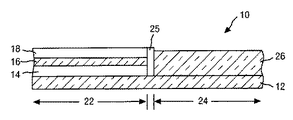
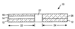
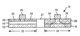
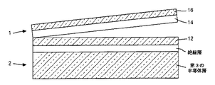
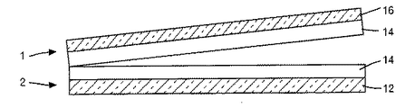
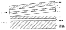
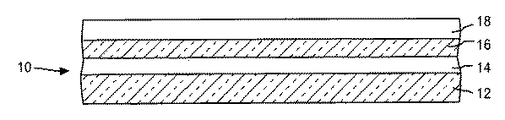
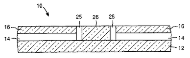
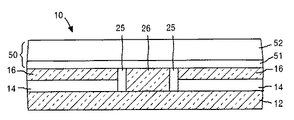
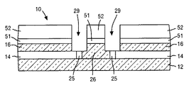
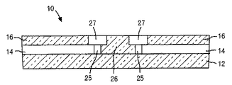
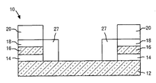
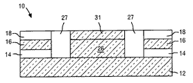
12 第2の半導体層
14 絶縁層
16 第1の半導体層
18 表面誘電体層
20 マスク
22 第1のデバイス領域
24 第2のデバイス領域
25 スペーサ(ライナ)
26 半導体材料
27 分離領域
29 トレンチ開口
30 第1の半導体デバイス
31 歪Si層
32 第2の半導体デバイス
34 ソース/ドレイン拡散領域
Claims (39)
- 少なくとも2つのタイプの結晶方位を有する基板と、
第1のタイプの結晶方位を有する前記基板の第1の部分の上に形成された第1のタイプのトランジスタと、
第2のタイプの結晶方位を有する前記基板の第2の部分の上に形成された第2のタイプのトランジスタとを含む集積回路構造であって、
前記基板の前記第1の部分のうち選択された部分が、非浮遊基板部分を含み、
前記基板の前記第1の部分の残りの部分と前記第2の部分の全てとが、浮遊基板部分を含む、集積回路構造。 - 前記浮遊基板部分が、シリコン・オン・インシュレータ(SOI)構造を含む、請求項1に記載の構造。
- 前記非浮遊基板部分が、前記基板の下の層によってバイアスされる、請求項1に記載の構造。
- 前記浮遊基板部分の下に完全な絶縁層をさらに含む、請求項1に記載の構造。
- 前記非浮遊基板部分の下に不完全な絶縁層をさらに含む、請求項1に記載の構造。
- 前記非浮遊基板部分と前記浮遊基板部分の間に浅いトレンチ分離(STI)領域をさらに含む、請求項1に記載の構造。
- 前記基板の前記第2の部分がそれぞれ複数の浮遊基板部分を含む、請求項1に記載の構造。
- 少なくとも2つのタイプの結晶方位を有する基板と、
第1のタイプの結晶方位を有する前記基板の第1の部分の上に形成されたN型トランジスタと、
第2のタイプの結晶方位を有する前記基板の第2の部分の上に形成されたP型トランジスタとを含む集積回路構造であって、
前記基板の前記第1の部分のうち選択された部分が、非浮遊基板部分を含み、
前記基板の前記第1の部分の残りの部分と前記第2の部分の全てとが、浮遊基板部分を含む、集積回路構造。 - 前記浮遊基板部分が、シリコン・オン・インシュレータ(SOI)構造を含む、請求項8に記載の構造。
- 前記非浮遊基板部分が、前記基板の下の層によってバイアスされる、請求項8に記載の構造。
- 前記浮遊基板部分の下に完全な(全て絶縁体の)絶縁層をさらに含む、請求項8に記載の構造。
- 前記非浮遊基板部分の下に不完全な絶縁層をさらに含む、請求項8に記載の構造。
- 前記非浮遊基板部分と前記浮遊基板部分の間に浅いトレンチ分離(STI)領域をさらに含む、請求項8に記載の構造。
- 前記基板の前記第2の部分がそれぞれ複数の浮遊基板部分を含む、請求項8に記載の構造。
- 集積回路構造を形成する方法であって、
第1の基板構造上に絶縁層を形成するステップと、
前記絶縁層に第2の基板構造を接合して、前記絶縁層の下に位置する第1の結晶方位を有する第1の基板および前記絶縁層の上に位置する第2の結晶方位を有する第2の基板を備える積層構造を形成するステップと、
前記第2の基板に、前記絶縁層まで延びる第1の開口を形成するステップと、
前記第1の開口より小さい第2の開口を前記第1の開口を貫通して前記絶縁層に形成して前記第1の基板を露出させるステップと、
前記第2の開口を貫通して前記第1の基板上に追加の材料を成長させて前記第1の開口を充填し、前記積層構造の上部に、前記第1のタイプの結晶方位を有する第1の部分および前記第2のタイプの結晶方位を有する第2の部分を備える表面を形成するステップと、
前記表面の前記第1の部分の上に第1のタイプのトランジスタを形成するステップと、
前記表面の前記第2の部分の上に第2のタイプのトランジスタを形成するステップとを含み、
前記表面の前記第1の部分のうち前記絶縁層の前記第2の開口の上に形成された部分が、非浮遊基板部分を含み、
前記表面の前記第1の部分の残りの部分と前記第2の部分の全てとが、浮遊基板部分を含む、方法。 - 前記追加の材料が、前記第1の基板と同じ結晶方位を有する、請求項15に記載の方法。
- 前記第1の開口を形成する前記ステップの前に、前記第2の基板を覆う保護キャップを形成するステップをさらに含み、前記第1の開口が、前記保護キャップおよび前記第2の基板を貫通して形成される、請求項15に記載の方法。
- 前記第1の開口を形成した後に、前記第1の開口によって露出した前記第2の基板の側壁に沿って分離材料を形成するステップをさらに含む、請求項15に記載の方法。
- 前記追加の材料を成長させる前記ステップの後に、前記第1の部分および前記第2の部分に浅いトレンチ分離(STI)構造を形成して前記第1の部分および前記第2の部分を細分割するステップをさらに含む、請求項15に記載の方法。
- 前記第2の開口が前記浅いトレンチ分離構造の間の距離よりも小さくすることにより、前記第2の開口のそれぞれが隣接する2つの浅いトレンチ分離構造の間に位置するようになっている、請求項15に記載の方法。
- 1タイプの結晶方位を有する材料を含む基板であって、第1の部分および第2の部分を含み、前記第1の部分の結晶構造が前記第2の部分の結晶構造に対して回転している基板と、
前記基板の前記第1の部分の上に形成された、第1のタイプのフィン型電界効果トランジスタ(FinFET)と、
前記基板の前記第2の部分の上に形成された第2のタイプのフィン型電界効果トランジスタとを含む集積回路構造であって、
前記第1のタイプのフィン型電界効果トランジスタが、前記第2のタイプのフィン型電界効果トランジスタのフィンと平行なフィンを有する、集積回路構造。 - 前記基板が浮遊基板を含む、請求項21に記載の構造。
- 前記第1のタイプのフィン型電界効果トランジスタおよび前記第2のタイプのフィン型電界効果トランジスタが、シリコン・オン・インシュレータ(SOI)構造を含む、請求項22に記載の構造。
- 前記浮遊基板の下に完全な絶縁層をさらに含む、請求項22に記載の構造。
- 前記基板の前記第1の部分と前記基板の前記第2の部分の間に、浅いトレンチ分離(STI)領域をさらに含む、請求項22に記載の構造。
- 集積回路構造を形成する方法であって、
第1の基板構造上に絶縁層を形成するステップと、
前記絶縁層に第2の基板構造を接合して、前記第1の基板構造と前記第2の基板構造の間に前記絶縁層を有する積層構造を形成するステップであって、前記第1の基板構造および前記第2の基板構造が同じタイプの結晶方位を有し、前記第1の基板構造の結晶構造が前記第2の基板構造の結晶構造に対して回転しているステップと、
前記第1の基板構造に、前記第2の基板構造まで延びる開口を形成するステップと、
前記開口を貫通して前記第2の基板構造上に材料を成長させて前記開口を充填して、前記積層構造の上部に、第1の部分および第2の部分を有する表面を形成するステップであって、前記第1の部分の結晶構造が前記第2の部分の結晶構造に対して回転しているステップと、
前記表面の前記第1の部分の上に第1のタイプのフィン型電界効果トランジスタを形成するステップと、
前記表面の前記第2の部分の上に第2のタイプのフィン型電界効果トランジスタを形成するステップとを含む方法。 - 前記開口を形成するステップの後に、前記開口の側壁に沿って分離材料を形成するステップをさらに含む、請求項26に記載の方法。
- 前記材料を成長させる前記ステップの後に、前記第1の部分および前記第2の部分に浅いトレンチ分離(STI)構造を形成して前記第1の部分および前記第2の部分を細分割するステップをさらに含む、請求項26に記載の方法。
- 集積回路構造を形成する方法であって、
第1の基板構造上に絶縁層を形成するステップと、
前記絶縁層に第2の基板構造を接合して、前記第1の基板構造と前記第2の基板構造の間に前記絶縁層を有する積層構造を形成するステップであって、前記第1の基板構造および前記第2の基板構造が同じタイプの結晶方位を有し、前記第1の基板構造の結晶構造が前記第2の基板構造の結晶構造に対して回転しているステップと、
前記第2の基板に、前記絶縁層まで延びる第1の開口を形成するステップと、
前記第1の開口より小さい第2の開口を前記第1の開口を貫通して前記絶縁層に形成して前記第1の基板構造を露出させるステップと、
前記第2の開口を貫通して前記第1の基板構造上に材料を成長させて前記第1の開口を充填して、前記積層構造の上部に、第1の部分および第2の部分を有する表面を形成するステップであって、前記第1の部分の結晶構造が前記第2の部分の結晶構造に対して回転しているステップと、
前記表面の前記第1の部分の上に第1のタイプのフィン型電界効果トランジスタ(FinFET)を形成するステップと、
前記表面の前記第2の部分の上に第2のタイプのフィン型電界効果トランジスタを形成するステップとを含み、
前記表面の前記第1の部分のうち前記絶縁層の前記第2の開口の上に形成された部分が、非浮遊基板部分を含み、
前記表面の前記第1の部分の残りの部分と前記第2の部分の全てとが、浮遊基板部分を含む、方法。 - 前記第1の開口を形成する前記ステップの前に、前記第2の基板構造を覆う保護キャップを形成するステップをさらに含み、前記第1の開口が、前記保護キャップおよび前記第2の基板を貫通して形成される、請求項29に記載の方法。
- 前記第1の開口を形成するステップの後に、前記第1の開口によって露出した前記第2の基板の側壁に沿って分離材料を形成するステップをさらに含む、請求項29に記載の方法。
- 前記材料を成長させる前記ステップの後に、前記第1の部分および前記第2の部分に浅いトレンチ分離(STI)構造を形成して前記第1の部分および前記第2の部分を細分割するステップをさらに含む、請求項29に記載の方法。
- 前記第1の基板が、前記第2の基板に対して45°回転している、請求項29に記載の方法。
- 集積回路構造を形成する方法であって、
第1の結晶方位を有する第1の基板構造上に絶縁層を形成するステップと、
第2の結晶方位を有する第2の基板構造を前記絶縁層に接合して、積層構造を形成するステップと、
前記第1の基板構造および前記絶縁層に開口を形成して、前記第2の基板構造の一部分を露出させるステップと、
前記第2の基板構造の露出部分の上にシリコン・ゲルマニウム層を形成するステップと、
前記開口を貫通して前記シリコン・ゲルマニウム層の上に材料を成長させて前記開口を充填し、前記積層構造の上部に、前記第1の結晶方位を有する第1の部分および前記第2の結晶方位を有する第2の部分を有する表面を形成するステップと、
前記第1の部分および前記第2の部分をパターン形成して第1のタイプのフィンおよび第2のタイプのフィンを形成するステップであって、前記第1のタイプのフィンは前記第1の結晶方位を有し、かつ前記絶縁層によって前記第2の基板から絶縁され、前記第2のタイプのフィンは前記第2の結晶方位を有し、かつ前記シリコン・ゲルマニウム層の上に位置するステップと、
前記シリコン・ゲルマニウム層を絶縁層に変化させるステップとを含む方法。 - 前記シリコン・ゲルマニウム層を形成するステップの前に、さらに追加の絶縁層を用いて、前記開口内の前記第1の基板の露出した側壁部分を保護するステップをさらに含む、請求項34に記載の方法。
- 前記シリコン・ゲルマニウム層を絶縁層に変化させる前記ステップが、前記シリコン・ゲルマニウム層の全厚にわたってを酸化することを含む、請求項34に記載の方法。
- 前記シリコン・ゲルマニウム層を絶縁層に変化させる前記ステップが、
前記第1のタイプのフィンおよび前記第2のタイプのフィンについて選択的に前記シリコン・ゲルマニウムを除去するステップと、
前記第2の基板構造上に前記絶縁層を形成するステップとを含む、請求項34に記載の方法。 - 前記第1の基板構造および前記第2の基板構造が、同じタイプの結晶方位を有し、前記第1の基板構造の結晶構造が、前記第2の基板構造の結晶構造に対して回転している、請求項34に記載の方法。
- 前記第1の基板構造および前記第2の基板構造が、異なるタイプの結晶方位を有する、請求項34に記載の方法。
Applications Claiming Priority (1)
| Application Number | Priority Date | Filing Date | Title |
|---|---|---|---|
| US10/708,907 US6998684B2 (en) | 2004-03-31 | 2004-03-31 | High mobility plane CMOS SOI |
Publications (2)
| Publication Number | Publication Date |
|---|---|
| JP2005294828A true JP2005294828A (ja) | 2005-10-20 |
| JP4243671B2 JP4243671B2 (ja) | 2009-03-25 |
Family
ID=35059712
Family Applications (1)
| Application Number | Title | Priority Date | Filing Date |
|---|---|---|---|
| JP2005085789A Expired - Fee Related JP4243671B2 (ja) | 2004-03-31 | 2005-03-24 | 集積回路構造及び形成方法 |
Country Status (4)
| Country | Link |
|---|---|
| US (2) | US6998684B2 (ja) |
| JP (1) | JP4243671B2 (ja) |
| CN (1) | CN100367500C (ja) |
| TW (1) | TWI332251B (ja) |
Cited By (10)
| Publication number | Priority date | Publication date | Assignee | Title |
|---|---|---|---|---|
| KR100741468B1 (ko) | 2006-07-10 | 2007-07-20 | 삼성전자주식회사 | 반도체 장치 및 그 형성 방법 |
| JP2008503104A (ja) * | 2004-06-10 | 2008-01-31 | フリースケール セミコンダクター インコーポレイテッド | 複数の半導体層を備えた半導体デバイス |
| JP2008131033A (ja) * | 2006-11-20 | 2008-06-05 | Internatl Business Mach Corp <Ibm> | 正孔移動度を向上させる方法 |
| JP2008141177A (ja) * | 2006-11-30 | 2008-06-19 | Internatl Business Mach Corp <Ibm> | 異なる垂直寸法のフィンを有するトリプル・ゲート・フィンfetおよびダブル・ゲート・フィンfet |
| JP2008211052A (ja) * | 2007-02-27 | 2008-09-11 | Toshiba Corp | 相補型半導体装置 |
| JP2009054705A (ja) * | 2007-08-24 | 2009-03-12 | Toshiba Corp | 半導体基板、半導体装置およびその製造方法 |
| JP2009514247A (ja) * | 2005-10-31 | 2009-04-02 | フリースケール セミコンダクター インコーポレイテッド | 半導体構造物の製造方法 |
| JP2013508951A (ja) * | 2009-10-16 | 2013-03-07 | ナショナル セミコンダクター コーポレーション | HOT(hybridorientationtechnology)を選択的エピタキシーに関連して用いて移動度を改善する方法およびそれに関連する装置 |
| JP2018182146A (ja) * | 2017-04-17 | 2018-11-15 | 株式会社Sumco | 多層膜soiウェーハの製造方法および多層膜soiウェーハ |
| JP2022515592A (ja) * | 2019-01-02 | 2022-02-21 | インターナショナル・ビジネス・マシーンズ・コーポレーション | 積層垂直輸送電界効果トランジスタのための2重輸送配向 |
Families Citing this family (81)
| Publication number | Priority date | Publication date | Assignee | Title |
|---|---|---|---|---|
| US7094634B2 (en) * | 2004-06-30 | 2006-08-22 | International Business Machines Corporation | Structure and method for manufacturing planar SOI substrate with multiple orientations |
| US7439542B2 (en) * | 2004-10-05 | 2008-10-21 | International Business Machines Corporation | Hybrid orientation CMOS with partial insulation process |
| US7144785B2 (en) * | 2004-11-01 | 2006-12-05 | Advanced Micro Devices, Inc. | Method of forming isolation trench with spacer formation |
| US7393733B2 (en) * | 2004-12-01 | 2008-07-01 | Amberwave Systems Corporation | Methods of forming hybrid fin field-effect transistor structures |
| US7196380B2 (en) * | 2005-01-13 | 2007-03-27 | International Business Machines Corporation | High mobility plane FinFET with equal drive strength |
| US7388278B2 (en) | 2005-03-24 | 2008-06-17 | International Business Machines Corporation | High performance field effect transistors on SOI substrate with stress-inducing material as buried insulator and methods |
| US7348611B2 (en) * | 2005-04-22 | 2008-03-25 | International Business Machines Corporation | Strained complementary metal oxide semiconductor (CMOS) on rotated wafers and methods thereof |
| US20060292719A1 (en) * | 2005-05-17 | 2006-12-28 | Amberwave Systems Corporation | Lattice-mismatched semiconductor structures with reduced dislocation defect densities and related methods for device fabrication |
| US8324660B2 (en) | 2005-05-17 | 2012-12-04 | Taiwan Semiconductor Manufacturing Company, Ltd. | Lattice-mismatched semiconductor structures with reduced dislocation defect densities and related methods for device fabrication |
| US9153645B2 (en) * | 2005-05-17 | 2015-10-06 | Taiwan Semiconductor Manufacturing Company, Ltd. | Lattice-mismatched semiconductor structures with reduced dislocation defect densities and related methods for device fabrication |
| US20070267722A1 (en) * | 2006-05-17 | 2007-11-22 | Amberwave Systems Corporation | Lattice-mismatched semiconductor structures with reduced dislocation defect densities and related methods for device fabrication |
| FR2886763B1 (fr) * | 2005-06-06 | 2007-08-03 | Commissariat Energie Atomique | Procede de realisation d'un composant comportant au moins un element a base de germanium et composant ainsi obtenu |
| US7473985B2 (en) * | 2005-06-16 | 2009-01-06 | International Business Machines Corporation | Hybrid oriented substrates and crystal imprinting methods for forming such hybrid oriented substrates |
| US7358164B2 (en) * | 2005-06-16 | 2008-04-15 | International Business Machines Corporation | Crystal imprinting methods for fabricating substrates with thin active silicon layers |
| US7439108B2 (en) * | 2005-06-16 | 2008-10-21 | International Business Machines Corporation | Coplanar silicon-on-insulator (SOI) regions of different crystal orientations and methods of making the same |
| US7190050B2 (en) * | 2005-07-01 | 2007-03-13 | Synopsys, Inc. | Integrated circuit on corrugated substrate |
| US7247887B2 (en) * | 2005-07-01 | 2007-07-24 | Synopsys, Inc. | Segmented channel MOS transistor |
| US7265008B2 (en) | 2005-07-01 | 2007-09-04 | Synopsys, Inc. | Method of IC production using corrugated substrate |
| CN101268547B (zh) * | 2005-07-26 | 2014-07-09 | 琥珀波系统公司 | 包含交替有源区材料的结构及其形成方法 |
| US7382029B2 (en) * | 2005-07-29 | 2008-06-03 | International Business Machines Corporation | Method and apparatus for improving integrated circuit device performance using hybrid crystal orientations |
| KR100655437B1 (ko) * | 2005-08-09 | 2006-12-08 | 삼성전자주식회사 | 반도체 웨이퍼 및 그 제조방법 |
| US7638842B2 (en) * | 2005-09-07 | 2009-12-29 | Amberwave Systems Corporation | Lattice-mismatched semiconductor structures on insulators |
| US7986029B2 (en) * | 2005-11-08 | 2011-07-26 | Taiwan Semiconductor Manufacturing Company, Ltd. | Dual SOI structure |
| US8319285B2 (en) * | 2005-12-22 | 2012-11-27 | Infineon Technologies Ag | Silicon-on-insulator chip having multiple crystal orientations |
| US7531392B2 (en) * | 2006-02-27 | 2009-05-12 | International Business Machines Corporation | Multi-orientation semiconductor-on-insulator (SOI) substrate, and method of fabricating same |
| US20070215984A1 (en) * | 2006-03-15 | 2007-09-20 | Shaheen Mohamad A | Formation of a multiple crystal orientation substrate |
| US7777250B2 (en) | 2006-03-24 | 2010-08-17 | Taiwan Semiconductor Manufacturing Company, Ltd. | Lattice-mismatched semiconductor structures and related methods for device fabrication |
| US8946811B2 (en) * | 2006-07-10 | 2015-02-03 | Taiwan Semiconductor Manufacturing Company, Ltd. | Body-tied, strained-channel multi-gate device and methods of manufacturing same |
| US8173551B2 (en) | 2006-09-07 | 2012-05-08 | Taiwan Semiconductor Manufacturing Co., Ltd. | Defect reduction using aspect ratio trapping |
| WO2008036256A1 (en) * | 2006-09-18 | 2008-03-27 | Amberwave Systems Corporation | Aspect ratio trapping for mixed signal applications |
| US7875958B2 (en) | 2006-09-27 | 2011-01-25 | Taiwan Semiconductor Manufacturing Company, Ltd. | Quantum tunneling devices and circuits with lattice-mismatched semiconductor structures |
| WO2008039495A1 (en) * | 2006-09-27 | 2008-04-03 | Amberwave Systems Corporation | Tri-gate field-effect transistors formed by aspect ratio trapping |
| WO2008051503A2 (en) | 2006-10-19 | 2008-05-02 | Amberwave Systems Corporation | Light-emitter-based devices with lattice-mismatched semiconductor structures |
| US7393738B1 (en) | 2007-01-16 | 2008-07-01 | International Business Machines Corporation | Subground rule STI fill for hot structure |
| FR2913528B1 (fr) | 2007-03-06 | 2009-07-03 | Soitec Silicon On Insulator | Procede de fabrication d'un substrat comportant une couche d'oxyde enterree pour la realisation de composants electroniques ou analogues. |
| US7825328B2 (en) | 2007-04-09 | 2010-11-02 | Taiwan Semiconductor Manufacturing Company, Ltd. | Nitride-based multi-junction solar cell modules and methods for making the same |
| US8304805B2 (en) | 2009-01-09 | 2012-11-06 | Taiwan Semiconductor Manufacturing Company, Ltd. | Semiconductor diodes fabricated by aspect ratio trapping with coalesced films |
| WO2008124154A2 (en) | 2007-04-09 | 2008-10-16 | Amberwave Systems Corporation | Photovoltaics on silicon |
| US8237151B2 (en) | 2009-01-09 | 2012-08-07 | Taiwan Semiconductor Manufacturing Company, Ltd. | Diode-based devices and methods for making the same |
| US8329541B2 (en) | 2007-06-15 | 2012-12-11 | Taiwan Semiconductor Manufacturing Company, Ltd. | InP-based transistor fabrication |
| DE112008002387B4 (de) | 2007-09-07 | 2022-04-07 | Taiwan Semiconductor Manufacturing Co., Ltd. | Struktur einer Mehrfachübergangs-Solarzelle, Verfahren zur Bildung einer photonischenVorrichtung, Photovoltaische Mehrfachübergangs-Zelle und Photovoltaische Mehrfachübergangs-Zellenvorrichtung, |
| EP2065921A1 (en) * | 2007-11-29 | 2009-06-03 | S.O.I.T.E.C. Silicon on Insulator Technologies | Method for fabricating a semiconductor substrate with areas with different crystal orienation |
| EP2073267A1 (en) * | 2007-12-19 | 2009-06-24 | INTERUNIVERSITAIR MICROELEKTRONICA CENTRUM vzw (IMEC) | Method of fabricating multi-gate semiconductor devices and devices obtained |
| US7982269B2 (en) * | 2008-04-17 | 2011-07-19 | International Business Machines Corporation | Transistors having asymmetric strained source/drain portions |
| US8106459B2 (en) | 2008-05-06 | 2012-01-31 | Taiwan Semiconductor Manufacturing Company, Ltd. | FinFETs having dielectric punch-through stoppers |
| US8183667B2 (en) | 2008-06-03 | 2012-05-22 | Taiwan Semiconductor Manufacturing Co., Ltd. | Epitaxial growth of crystalline material |
| KR101046380B1 (ko) * | 2008-06-05 | 2011-07-05 | 주식회사 하이닉스반도체 | 반도체 소자 및 그의 제조방법 |
| US8274097B2 (en) | 2008-07-01 | 2012-09-25 | Taiwan Semiconductor Manufacturing Company, Ltd. | Reduction of edge effects from aspect ratio trapping |
| US8981427B2 (en) | 2008-07-15 | 2015-03-17 | Taiwan Semiconductor Manufacturing Company, Ltd. | Polishing of small composite semiconductor materials |
| US20100072515A1 (en) | 2008-09-19 | 2010-03-25 | Amberwave Systems Corporation | Fabrication and structures of crystalline material |
| CN102160145B (zh) | 2008-09-19 | 2013-08-21 | 台湾积体电路制造股份有限公司 | 通过外延层过成长的元件形成 |
| US8253211B2 (en) | 2008-09-24 | 2012-08-28 | Taiwan Semiconductor Manufacturing Company, Ltd. | Semiconductor sensor structures with reduced dislocation defect densities |
| US8263462B2 (en) * | 2008-12-31 | 2012-09-11 | Taiwan Semiconductor Manufacturing Company, Ltd. | Dielectric punch-through stoppers for forming FinFETs having dual fin heights |
| US8293616B2 (en) | 2009-02-24 | 2012-10-23 | Taiwan Semiconductor Manufacturing Company, Ltd. | Methods of fabrication of semiconductor devices with low capacitance |
| JP5705207B2 (ja) * | 2009-04-02 | 2015-04-22 | 台湾積體電路製造股▲ふん▼有限公司Taiwan Semiconductor Manufacturing Company,Ltd. | 結晶物質の非極性面から形成される装置とその製作方法 |
| CN102790054B (zh) * | 2011-05-16 | 2015-09-16 | 中国科学院上海微系统与信息技术研究所 | 锗和iii-v混合共平面的半导体结构及其制备方法 |
| US8697522B2 (en) * | 2011-07-05 | 2014-04-15 | International Business Machines Corporation | Bulk finFET with uniform height and bottom isolation |
| CN106847805B (zh) * | 2011-12-23 | 2020-08-21 | 英特尔公司 | 具有包含不同材料取向或组成的纳米线或半导体主体的共衬底半导体器件 |
| US8466012B1 (en) * | 2012-02-01 | 2013-06-18 | International Business Machines Corporation | Bulk FinFET and SOI FinFET hybrid technology |
| US9817928B2 (en) | 2012-08-31 | 2017-11-14 | Synopsys, Inc. | Latch-up suppression and substrate noise coupling reduction through a substrate back-tie for 3D integrated circuits |
| US9190346B2 (en) | 2012-08-31 | 2015-11-17 | Synopsys, Inc. | Latch-up suppression and substrate noise coupling reduction through a substrate back-tie for 3D integrated circuits |
| CN103715091A (zh) * | 2012-09-29 | 2014-04-09 | 中芯国际集成电路制造(上海)有限公司 | 半导体基底、晶体管和鳍部的形成方法 |
| US9275911B2 (en) | 2012-10-12 | 2016-03-01 | Globalfoundries Inc. | Hybrid orientation fin field effect transistor and planar field effect transistor |
| US8847324B2 (en) | 2012-12-17 | 2014-09-30 | Synopsys, Inc. | Increasing ION /IOFF ratio in FinFETs and nano-wires |
| US9379018B2 (en) | 2012-12-17 | 2016-06-28 | Synopsys, Inc. | Increasing Ion/Ioff ratio in FinFETs and nano-wires |
| US8906768B2 (en) * | 2013-03-15 | 2014-12-09 | GlobalFoundries, Inc. | Wrap around stressor formation |
| US9396931B2 (en) * | 2013-08-01 | 2016-07-19 | Qualcomm Incorporated | Method of forming fins from different materials on a substrate |
| US9224841B2 (en) * | 2014-01-23 | 2015-12-29 | Globalfoundries Inc. | Semiconductor fins on a trench isolation region in a bulk semiconductor substrate and a method of forming the semiconductor fins |
| US9123585B1 (en) | 2014-02-11 | 2015-09-01 | International Business Machines Corporation | Method to form group III-V and Si/Ge FINFET on insulator |
| US9129863B2 (en) | 2014-02-11 | 2015-09-08 | International Business Machines Corporation | Method to form dual channel group III-V and Si/Ge FINFET CMOS |
| US9490161B2 (en) * | 2014-04-29 | 2016-11-08 | International Business Machines Corporation | Channel SiGe devices with multiple threshold voltages on hybrid oriented substrates, and methods of manufacturing same |
| EP2947693B1 (en) | 2014-05-22 | 2022-07-13 | IMEC vzw | Method of Producing a III-V Fin Structure |
| US10056293B2 (en) * | 2014-07-18 | 2018-08-21 | International Business Machines Corporation | Techniques for creating a local interconnect using a SOI wafer |
| US10411135B2 (en) | 2015-06-08 | 2019-09-10 | Synopsys, Inc. | Substrates and transistors with 2D material channels on 3D geometries |
| CN104966672B (zh) * | 2015-06-30 | 2019-01-25 | 上海华力微电子有限公司 | 鳍式场效应管基体制备方法 |
| US9935106B2 (en) | 2016-04-01 | 2018-04-03 | Globalfoundries Inc. | Multi-finger devices in mutliple-gate-contacted-pitch, integrated structures |
| US9847418B1 (en) * | 2016-07-26 | 2017-12-19 | Globalfoundries Inc. | Methods of forming fin cut regions by oxidizing fin portions |
| CN106711194B (zh) * | 2016-12-28 | 2019-08-20 | 中国科学院微电子研究所 | 一种环栅场效应晶体管及其制备方法 |
| US10930569B2 (en) * | 2018-07-31 | 2021-02-23 | Taiwan Semiconductor Manufacturing Co., Ltd. | Dual crystal orientation for semiconductor devices |
| CN111799365B (zh) * | 2020-06-29 | 2022-03-25 | 上海新硅聚合半导体有限公司 | 基于同一衬底制备不同厚度薄膜的方法及其结构、及应用器件 |
| CN112563332A (zh) * | 2020-12-16 | 2021-03-26 | 南京工程学院 | Ge基双栅型InGaAs nMOSFET器件及其制备方法 |
Family Cites Families (9)
| Publication number | Priority date | Publication date | Assignee | Title |
|---|---|---|---|---|
| JPH01162376A (ja) * | 1987-12-18 | 1989-06-26 | Fujitsu Ltd | 半導体装置の製造方法 |
| US5959335A (en) * | 1998-09-23 | 1999-09-28 | International Business Machines Corporation | Device design for enhanced avalanche SOI CMOS |
| JP2001111056A (ja) * | 1999-10-06 | 2001-04-20 | Mitsubishi Electric Corp | 半導体装置およびその製造方法 |
| US6657259B2 (en) * | 2001-12-04 | 2003-12-02 | International Business Machines Corporation | Multiple-plane FinFET CMOS |
| US6657223B1 (en) | 2002-10-29 | 2003-12-02 | Advanced Micro Devices, Inc. | Strained silicon MOSFET having silicon source/drain regions and method for its fabrication |
| US6794718B2 (en) * | 2002-12-19 | 2004-09-21 | International Business Machines Corporation | High mobility crystalline planes in double-gate CMOS technology |
| US6900502B2 (en) | 2003-04-03 | 2005-05-31 | Taiwan Semiconductor Manufacturing Company, Ltd. | Strained channel on insulator device |
| US6902962B2 (en) | 2003-04-04 | 2005-06-07 | Taiwan Semiconductor Manufacturing Company, Ltd. | Silicon-on-insulator chip with multiple crystal orientations |
| US6995456B2 (en) * | 2004-03-12 | 2006-02-07 | International Business Machines Corporation | High-performance CMOS SOI devices on hybrid crystal-oriented substrates |
-
2004
- 2004-03-31 US US10/708,907 patent/US6998684B2/en not_active Expired - Lifetime
-
2005
- 2005-03-24 CN CNB2005100591708A patent/CN100367500C/zh not_active Expired - Lifetime
- 2005-03-24 JP JP2005085789A patent/JP4243671B2/ja not_active Expired - Fee Related
- 2005-03-25 TW TW094109281A patent/TWI332251B/zh not_active IP Right Cessation
- 2005-11-09 US US11/270,708 patent/US7439109B2/en not_active Expired - Fee Related
Cited By (13)
| Publication number | Priority date | Publication date | Assignee | Title |
|---|---|---|---|---|
| JP2008503104A (ja) * | 2004-06-10 | 2008-01-31 | フリースケール セミコンダクター インコーポレイテッド | 複数の半導体層を備えた半導体デバイス |
| JP2009514247A (ja) * | 2005-10-31 | 2009-04-02 | フリースケール セミコンダクター インコーポレイテッド | 半導体構造物の製造方法 |
| KR100741468B1 (ko) | 2006-07-10 | 2007-07-20 | 삼성전자주식회사 | 반도체 장치 및 그 형성 방법 |
| JP2008131033A (ja) * | 2006-11-20 | 2008-06-05 | Internatl Business Mach Corp <Ibm> | 正孔移動度を向上させる方法 |
| JP2008141177A (ja) * | 2006-11-30 | 2008-06-19 | Internatl Business Mach Corp <Ibm> | 異なる垂直寸法のフィンを有するトリプル・ゲート・フィンfetおよびダブル・ゲート・フィンfet |
| JP2013179343A (ja) * | 2006-11-30 | 2013-09-09 | Internatl Business Mach Corp <Ibm> | 異なる垂直寸法のフィンを有するトリプル・ゲート・フィンfetおよびダブル・ゲート・フィンfet |
| JP2008211052A (ja) * | 2007-02-27 | 2008-09-11 | Toshiba Corp | 相補型半導体装置 |
| JP2009054705A (ja) * | 2007-08-24 | 2009-03-12 | Toshiba Corp | 半導体基板、半導体装置およびその製造方法 |
| US8039843B2 (en) | 2007-08-24 | 2011-10-18 | Kabushiki Kaisha Toshiba | Semiconductor wafer, semiconductor device and method of fabricating the same |
| JP2013508951A (ja) * | 2009-10-16 | 2013-03-07 | ナショナル セミコンダクター コーポレーション | HOT(hybridorientationtechnology)を選択的エピタキシーに関連して用いて移動度を改善する方法およびそれに関連する装置 |
| JP2018182146A (ja) * | 2017-04-17 | 2018-11-15 | 株式会社Sumco | 多層膜soiウェーハの製造方法および多層膜soiウェーハ |
| JP2022515592A (ja) * | 2019-01-02 | 2022-02-21 | インターナショナル・ビジネス・マシーンズ・コーポレーション | 積層垂直輸送電界効果トランジスタのための2重輸送配向 |
| JP7422765B2 (ja) | 2019-01-02 | 2024-01-26 | インターナショナル・ビジネス・マシーンズ・コーポレーション | 積層垂直輸送電界効果トランジスタのための2重輸送配向 |
Also Published As
| Publication number | Publication date |
|---|---|
| US20060076623A1 (en) | 2006-04-13 |
| US6998684B2 (en) | 2006-02-14 |
| CN1681124A (zh) | 2005-10-12 |
| TWI332251B (en) | 2010-10-21 |
| JP4243671B2 (ja) | 2009-03-25 |
| US7439109B2 (en) | 2008-10-21 |
| CN100367500C (zh) | 2008-02-06 |
| US20050224875A1 (en) | 2005-10-13 |
| TW200537648A (en) | 2005-11-16 |
Similar Documents
| Publication | Publication Date | Title |
|---|---|---|
| JP4243671B2 (ja) | 集積回路構造及び形成方法 | |
| US6995456B2 (en) | High-performance CMOS SOI devices on hybrid crystal-oriented substrates | |
| JP4931211B2 (ja) | ハイブリッド結晶配向基板上の高性能cmossoiデバイス | |
| US7915100B2 (en) | Hybrid orientation CMOS with partial insulation process | |
| US9355887B2 (en) | Dual trench isolation for CMOS with hybrid orientations | |
| KR100613188B1 (ko) | 웨이퍼 본딩 공정과 simox 공정을 이용하여 다른결정 방향을 갖는 자기 정렬된 soi | |
| US7023057B2 (en) | CMOS on hybrid substrate with different crystal orientations using silicon-to-silicon direct wafer bonding | |
| US7833854B2 (en) | Structure and method of fabricating a hybrid substrate for high-performance hybrid-orientation silicon-on-insulator CMOS devices | |
| US20050082531A1 (en) | Double silicon-on-insulator (SOI) metal oxide semiconductor field effect transistor (MOSFET) structures | |
| JP2008536335A (ja) | 適応ウェル・バイアシング、並びにパワー及び性能強化のためのハイブリッド結晶配向cmos構造体 | |
| US7393738B1 (en) | Subground rule STI fill for hot structure | |
| US7691482B2 (en) | Structure for planar SOI substrate with multiple orientations | |
| CN100361302C (zh) | 混合衬底、集成半导体结构以及它们的制备方法 |
Legal Events
| Date | Code | Title | Description |
|---|---|---|---|
| A977 | Report on retrieval |
Free format text: JAPANESE INTERMEDIATE CODE: A971007 Effective date: 20070808 |
|
| A131 | Notification of reasons for refusal |
Free format text: JAPANESE INTERMEDIATE CODE: A131 Effective date: 20070821 |
|
| A521 | Request for written amendment filed |
Free format text: JAPANESE INTERMEDIATE CODE: A821 Effective date: 20071120 Free format text: JAPANESE INTERMEDIATE CODE: A523 Effective date: 20071120 |
|
| RD12 | Notification of acceptance of power of sub attorney |
Free format text: JAPANESE INTERMEDIATE CODE: A7432 Effective date: 20071120 |
|
| A521 | Request for written amendment filed |
Free format text: JAPANESE INTERMEDIATE CODE: A821 Effective date: 20071121 |
|
| A131 | Notification of reasons for refusal |
Free format text: JAPANESE INTERMEDIATE CODE: A131 Effective date: 20080812 |
|
| A521 | Request for written amendment filed |
Free format text: JAPANESE INTERMEDIATE CODE: A523 Effective date: 20081110 Free format text: JAPANESE INTERMEDIATE CODE: A821 Effective date: 20081110 |
|
| TRDD | Decision of grant or rejection written | ||
| A521 | Request for written amendment filed |
Free format text: JAPANESE INTERMEDIATE CODE: A821 Effective date: 20081205 |
|
| RD14 | Notification of resignation of power of sub attorney |
Free format text: JAPANESE INTERMEDIATE CODE: A7434 Effective date: 20081205 |
|
| A01 | Written decision to grant a patent or to grant a registration (utility model) |
Free format text: JAPANESE INTERMEDIATE CODE: A01 Effective date: 20081205 |
|
| A01 | Written decision to grant a patent or to grant a registration (utility model) |
Free format text: JAPANESE INTERMEDIATE CODE: A01 |
|
| A521 | Request for written amendment filed |
Free format text: JAPANESE INTERMEDIATE CODE: A821 Effective date: 20081216 |
|
| RD14 | Notification of resignation of power of sub attorney |
Free format text: JAPANESE INTERMEDIATE CODE: A7434 Effective date: 20081216 |
|
| A61 | First payment of annual fees (during grant procedure) |
Free format text: JAPANESE INTERMEDIATE CODE: A61 Effective date: 20081210 |
|
| R150 | Certificate of patent or registration of utility model |
Free format text: JAPANESE INTERMEDIATE CODE: R150 |
|
| FPAY | Renewal fee payment (event date is renewal date of database) |
Free format text: PAYMENT UNTIL: 20120116 Year of fee payment: 3 |
|
| FPAY | Renewal fee payment (event date is renewal date of database) |
Free format text: PAYMENT UNTIL: 20130116 Year of fee payment: 4 |
|
| FPAY | Renewal fee payment (event date is renewal date of database) |
Free format text: PAYMENT UNTIL: 20140116 Year of fee payment: 5 |
|
| LAPS | Cancellation because of no payment of annual fees |