JP2005290076A - Epoxy resin composition and semiconductor device - Google Patents
Epoxy resin composition and semiconductor device Download PDFInfo
- Publication number
- JP2005290076A JP2005290076A JP2004103869A JP2004103869A JP2005290076A JP 2005290076 A JP2005290076 A JP 2005290076A JP 2004103869 A JP2004103869 A JP 2004103869A JP 2004103869 A JP2004103869 A JP 2004103869A JP 2005290076 A JP2005290076 A JP 2005290076A
- Authority
- JP
- Japan
- Prior art keywords
- epoxy resin
- resin composition
- spherical alumina
- spherical
- alumina
- Prior art date
- Legal status (The legal status is an assumption and is not a legal conclusion. Google has not performed a legal analysis and makes no representation as to the accuracy of the status listed.)
- Granted
Links
- 229920000647 polyepoxide Polymers 0.000 title claims abstract description 63
- 239000003822 epoxy resin Substances 0.000 title claims abstract description 62
- 239000004065 semiconductor Substances 0.000 title claims abstract description 49
- 239000000203 mixture Substances 0.000 title claims abstract description 42
- PNEYBMLMFCGWSK-UHFFFAOYSA-N aluminium oxide Inorganic materials [O-2].[O-2].[O-2].[Al+3].[Al+3] PNEYBMLMFCGWSK-UHFFFAOYSA-N 0.000 claims abstract description 78
- 239000002245 particle Substances 0.000 claims abstract description 59
- VYPSYNLAJGMNEJ-UHFFFAOYSA-N Silicium dioxide Chemical compound O=[Si]=O VYPSYNLAJGMNEJ-UHFFFAOYSA-N 0.000 claims abstract description 24
- 238000009826 distribution Methods 0.000 claims abstract description 19
- 238000005538 encapsulation Methods 0.000 claims abstract description 13
- 239000000377 silicon dioxide Substances 0.000 claims abstract description 11
- 239000005011 phenolic resin Substances 0.000 claims abstract description 10
- 238000002156 mixing Methods 0.000 claims description 7
- 239000004593 Epoxy Substances 0.000 claims description 3
- 239000011342 resin composition Substances 0.000 claims description 3
- 238000007789 sealing Methods 0.000 claims description 3
- 239000012798 spherical particle Substances 0.000 claims 1
- 239000011256 inorganic filler Substances 0.000 abstract description 13
- 229910003475 inorganic filler Inorganic materials 0.000 abstract description 13
- 230000000694 effects Effects 0.000 abstract description 6
- 230000017525 heat dissipation Effects 0.000 abstract description 5
- 230000002542 deteriorative effect Effects 0.000 abstract description 2
- 230000003750 conditioning effect Effects 0.000 abstract 1
- 238000005476 soldering Methods 0.000 abstract 1
- 238000000034 method Methods 0.000 description 15
- PCHJSUWPFVWCPO-UHFFFAOYSA-N gold Chemical compound [Au] PCHJSUWPFVWCPO-UHFFFAOYSA-N 0.000 description 9
- 229920005989 resin Polymers 0.000 description 8
- 239000011347 resin Substances 0.000 description 8
- 229910000679 solder Inorganic materials 0.000 description 8
- 229910052782 aluminium Inorganic materials 0.000 description 6
- XAGFODPZIPBFFR-UHFFFAOYSA-N aluminium Chemical compound [Al] XAGFODPZIPBFFR-UHFFFAOYSA-N 0.000 description 6
- -1 dicyclopentadiene modified phenol Chemical class 0.000 description 6
- 238000011049 filling Methods 0.000 description 6
- ISWSIDIOOBJBQZ-UHFFFAOYSA-N Phenol Chemical compound OC1=CC=CC=C1 ISWSIDIOOBJBQZ-UHFFFAOYSA-N 0.000 description 5
- 125000002887 hydroxy group Chemical group [H]O* 0.000 description 5
- 229920003986 novolac Polymers 0.000 description 5
- XLYOFNOQVPJJNP-UHFFFAOYSA-N water Substances O XLYOFNOQVPJJNP-UHFFFAOYSA-N 0.000 description 5
- 229910052581 Si3N4 Inorganic materials 0.000 description 4
- 230000002950 deficient Effects 0.000 description 4
- 238000004519 manufacturing process Methods 0.000 description 4
- 238000000465 moulding Methods 0.000 description 4
- 239000000843 powder Substances 0.000 description 4
- HQVNEWCFYHHQES-UHFFFAOYSA-N silicon nitride Chemical compound N12[Si]34N5[Si]62N3[Si]51N64 HQVNEWCFYHHQES-UHFFFAOYSA-N 0.000 description 4
- USFPINLPPFWTJW-UHFFFAOYSA-N tetraphenylphosphonium Chemical compound C1=CC=CC=C1[P+](C=1C=CC=CC=1)(C=1C=CC=CC=1)C1=CC=CC=C1 USFPINLPPFWTJW-UHFFFAOYSA-N 0.000 description 4
- 239000000919 ceramic Substances 0.000 description 3
- PMHQVHHXPFUNSP-UHFFFAOYSA-M copper(1+);methylsulfanylmethane;bromide Chemical compound Br[Cu].CSC PMHQVHHXPFUNSP-UHFFFAOYSA-M 0.000 description 3
- 239000007822 coupling agent Substances 0.000 description 3
- 125000003700 epoxy group Chemical group 0.000 description 3
- 238000011156 evaluation Methods 0.000 description 3
- 239000000945 filler Substances 0.000 description 3
- 230000001771 impaired effect Effects 0.000 description 3
- 238000002347 injection Methods 0.000 description 3
- 239000007924 injection Substances 0.000 description 3
- 238000005259 measurement Methods 0.000 description 3
- 239000000126 substance Substances 0.000 description 3
- 238000001721 transfer moulding Methods 0.000 description 3
- 239000001993 wax Substances 0.000 description 3
- IJGRMHOSHXDMSA-UHFFFAOYSA-N Atomic nitrogen Chemical compound N#N IJGRMHOSHXDMSA-UHFFFAOYSA-N 0.000 description 2
- BTBUEUYNUDRHOZ-UHFFFAOYSA-N Borate Chemical compound [O-]B([O-])[O-] BTBUEUYNUDRHOZ-UHFFFAOYSA-N 0.000 description 2
- QIGBRXMKCJKVMJ-UHFFFAOYSA-N Hydroquinone Chemical compound OC1=CC=C(O)C=C1 QIGBRXMKCJKVMJ-UHFFFAOYSA-N 0.000 description 2
- XYFCBTPGUUZFHI-UHFFFAOYSA-N Phosphine Chemical compound P XYFCBTPGUUZFHI-UHFFFAOYSA-N 0.000 description 2
- FKNQFGJONOIPTF-UHFFFAOYSA-N Sodium cation Chemical compound [Na+] FKNQFGJONOIPTF-UHFFFAOYSA-N 0.000 description 2
- 239000002253 acid Substances 0.000 description 2
- 239000000654 additive Substances 0.000 description 2
- ADCOVFLJGNWWNZ-UHFFFAOYSA-N antimony trioxide Chemical compound O=[Sb]O[Sb]=O ADCOVFLJGNWWNZ-UHFFFAOYSA-N 0.000 description 2
- 125000002529 biphenylenyl group Chemical group C1(=CC=CC=2C3=CC=CC=C3C12)* 0.000 description 2
- IISBACLAFKSPIT-UHFFFAOYSA-N bisphenol A Chemical compound C=1C=C(O)C=CC=1C(C)(C)C1=CC=C(O)C=C1 IISBACLAFKSPIT-UHFFFAOYSA-N 0.000 description 2
- PXKLMJQFEQBVLD-UHFFFAOYSA-N bisphenol F Chemical compound C1=CC(O)=CC=C1CC1=CC=C(O)C=C1 PXKLMJQFEQBVLD-UHFFFAOYSA-N 0.000 description 2
- 239000006229 carbon black Substances 0.000 description 2
- 239000004203 carnauba wax Substances 0.000 description 2
- 235000013869 carnauba wax Nutrition 0.000 description 2
- 239000003795 chemical substances by application Substances 0.000 description 2
- ZUOUZKKEUPVFJK-UHFFFAOYSA-N diphenyl Chemical compound C1=CC=CC=C1C1=CC=CC=C1 ZUOUZKKEUPVFJK-UHFFFAOYSA-N 0.000 description 2
- 238000000605 extraction Methods 0.000 description 2
- LNEPOXFFQSENCJ-UHFFFAOYSA-N haloperidol Chemical compound C1CC(O)(C=2C=CC(Cl)=CC=2)CCN1CCCC(=O)C1=CC=C(F)C=C1 LNEPOXFFQSENCJ-UHFFFAOYSA-N 0.000 description 2
- 150000002500 ions Chemical class 0.000 description 2
- 238000000691 measurement method Methods 0.000 description 2
- 238000002844 melting Methods 0.000 description 2
- 230000008018 melting Effects 0.000 description 2
- 239000000178 monomer Substances 0.000 description 2
- QWVGKYWNOKOFNN-UHFFFAOYSA-N o-cresol Chemical compound CC1=CC=CC=C1O QWVGKYWNOKOFNN-UHFFFAOYSA-N 0.000 description 2
- 150000002989 phenols Chemical class 0.000 description 2
- 229920000642 polymer Polymers 0.000 description 2
- 239000002994 raw material Substances 0.000 description 2
- 229910001415 sodium ion Inorganic materials 0.000 description 2
- 239000000758 substrate Substances 0.000 description 2
- RIOQSEWOXXDEQQ-UHFFFAOYSA-N triphenylphosphine Chemical compound C1=CC=CC=C1P(C=1C=CC=CC=1)C1=CC=CC=C1 RIOQSEWOXXDEQQ-UHFFFAOYSA-N 0.000 description 2
- JYEUMXHLPRZUAT-UHFFFAOYSA-N 1,2,3-triazine Chemical compound C1=CN=NN=C1 JYEUMXHLPRZUAT-UHFFFAOYSA-N 0.000 description 1
- YJTKZCDBKVTVBY-UHFFFAOYSA-N 1,3-Diphenylbenzene Chemical group C1=CC=CC=C1C1=CC=CC(C=2C=CC=CC=2)=C1 YJTKZCDBKVTVBY-UHFFFAOYSA-N 0.000 description 1
- XQUPVDVFXZDTLT-UHFFFAOYSA-N 1-[4-[[4-(2,5-dioxopyrrol-1-yl)phenyl]methyl]phenyl]pyrrole-2,5-dione Chemical compound O=C1C=CC(=O)N1C(C=C1)=CC=C1CC1=CC=C(N2C(C=CC2=O)=O)C=C1 XQUPVDVFXZDTLT-UHFFFAOYSA-N 0.000 description 1
- KJCVRFUGPWSIIH-UHFFFAOYSA-N 1-naphthol Chemical compound C1=CC=C2C(O)=CC=CC2=C1 KJCVRFUGPWSIIH-UHFFFAOYSA-N 0.000 description 1
- LXBGSDVWAMZHDD-UHFFFAOYSA-N 2-methyl-1h-imidazole Chemical compound CC1=NC=CN1 LXBGSDVWAMZHDD-UHFFFAOYSA-N 0.000 description 1
- QTWJRLJHJPIABL-UHFFFAOYSA-N 2-methylphenol;3-methylphenol;4-methylphenol Chemical compound CC1=CC=C(O)C=C1.CC1=CC=CC(O)=C1.CC1=CC=CC=C1O QTWJRLJHJPIABL-UHFFFAOYSA-N 0.000 description 1
- UUEWCQRISZBELL-UHFFFAOYSA-N 3-trimethoxysilylpropane-1-thiol Chemical compound CO[Si](OC)(OC)CCCS UUEWCQRISZBELL-UHFFFAOYSA-N 0.000 description 1
- 238000004438 BET method Methods 0.000 description 1
- VEXZGXHMUGYJMC-UHFFFAOYSA-M Chloride anion Chemical compound [Cl-] VEXZGXHMUGYJMC-UHFFFAOYSA-M 0.000 description 1
- KRHYYFGTRYWZRS-UHFFFAOYSA-M Fluoride anion Chemical compound [F-] KRHYYFGTRYWZRS-UHFFFAOYSA-M 0.000 description 1
- RMXQRHVIUMSGLJ-UHFFFAOYSA-N O.[Bi]=O Chemical compound O.[Bi]=O RMXQRHVIUMSGLJ-UHFFFAOYSA-N 0.000 description 1
- 239000004698 Polyethylene Substances 0.000 description 1
- BLRPTPMANUNPDV-UHFFFAOYSA-N Silane Chemical compound [SiH4] BLRPTPMANUNPDV-UHFFFAOYSA-N 0.000 description 1
- 239000006087 Silane Coupling Agent Substances 0.000 description 1
- 235000021355 Stearic acid Nutrition 0.000 description 1
- PJANXHGTPQOBST-VAWYXSNFSA-N Stilbene Natural products C=1C=CC=CC=1/C=C/C1=CC=CC=C1 PJANXHGTPQOBST-VAWYXSNFSA-N 0.000 description 1
- GWEVSGVZZGPLCZ-UHFFFAOYSA-N Titan oxide Chemical compound O=[Ti]=O GWEVSGVZZGPLCZ-UHFFFAOYSA-N 0.000 description 1
- RTAQQCXQSZGOHL-UHFFFAOYSA-N Titanium Chemical compound [Ti] RTAQQCXQSZGOHL-UHFFFAOYSA-N 0.000 description 1
- 238000002441 X-ray diffraction Methods 0.000 description 1
- QCWXUUIWCKQGHC-UHFFFAOYSA-N Zirconium Chemical compound [Zr] QCWXUUIWCKQGHC-UHFFFAOYSA-N 0.000 description 1
- 238000010521 absorption reaction Methods 0.000 description 1
- 239000002156 adsorbate Substances 0.000 description 1
- 150000001343 alkyl silanes Chemical class 0.000 description 1
- 229910045601 alloy Inorganic materials 0.000 description 1
- 239000000956 alloy Substances 0.000 description 1
- WNROFYMDJYEPJX-UHFFFAOYSA-K aluminium hydroxide Chemical compound [OH-].[OH-].[OH-].[Al+3] WNROFYMDJYEPJX-UHFFFAOYSA-K 0.000 description 1
- 239000003963 antioxidant agent Substances 0.000 description 1
- 230000003078 antioxidant effect Effects 0.000 description 1
- 235000010290 biphenyl Nutrition 0.000 description 1
- 239000004305 biphenyl Substances 0.000 description 1
- 150000001642 boronic acid derivatives Chemical class 0.000 description 1
- 238000011088 calibration curve Methods 0.000 description 1
- 238000006243 chemical reaction Methods 0.000 description 1
- 239000000460 chlorine Substances 0.000 description 1
- 239000003086 colorant Substances 0.000 description 1
- 230000000052 comparative effect Effects 0.000 description 1
- 238000000748 compression moulding Methods 0.000 description 1
- 238000007796 conventional method Methods 0.000 description 1
- 229930003836 cresol Natural products 0.000 description 1
- 239000013078 crystal Substances 0.000 description 1
- 229910002026 crystalline silica Inorganic materials 0.000 description 1
- 230000008021 deposition Effects 0.000 description 1
- 235000014113 dietary fatty acids Nutrition 0.000 description 1
- XXBDWLFCJWSEKW-UHFFFAOYSA-N dimethylbenzylamine Chemical compound CN(C)CC1=CC=CC=C1 XXBDWLFCJWSEKW-UHFFFAOYSA-N 0.000 description 1
- 239000008393 encapsulating agent Substances 0.000 description 1
- 238000005516 engineering process Methods 0.000 description 1
- 230000007613 environmental effect Effects 0.000 description 1
- 239000004744 fabric Substances 0.000 description 1
- 239000000194 fatty acid Substances 0.000 description 1
- 229930195729 fatty acid Natural products 0.000 description 1
- 150000004665 fatty acids Chemical class 0.000 description 1
- 239000003063 flame retardant Substances 0.000 description 1
- 239000007789 gas Substances 0.000 description 1
- 239000011521 glass Substances 0.000 description 1
- 238000000227 grinding Methods 0.000 description 1
- 150000002460 imidazoles Chemical class 0.000 description 1
- 239000012535 impurity Substances 0.000 description 1
- 239000004615 ingredient Substances 0.000 description 1
- 238000001746 injection moulding Methods 0.000 description 1
- 229910001410 inorganic ion Inorganic materials 0.000 description 1
- 238000007561 laser diffraction method Methods 0.000 description 1
- VTHJTEIRLNZDEV-UHFFFAOYSA-L magnesium dihydroxide Chemical compound [OH-].[OH-].[Mg+2] VTHJTEIRLNZDEV-UHFFFAOYSA-L 0.000 description 1
- 239000000347 magnesium hydroxide Substances 0.000 description 1
- 229910001862 magnesium hydroxide Inorganic materials 0.000 description 1
- 229910052751 metal Inorganic materials 0.000 description 1
- 239000002184 metal Substances 0.000 description 1
- UJNZOIKQAUQOCN-UHFFFAOYSA-N methyl(diphenyl)phosphane Chemical compound C=1C=CC=CC=1P(C)C1=CC=CC=C1 UJNZOIKQAUQOCN-UHFFFAOYSA-N 0.000 description 1
- 239000004570 mortar (masonry) Substances 0.000 description 1
- GKTNLYAAZKKMTQ-UHFFFAOYSA-N n-[bis(dimethylamino)phosphinimyl]-n-methylmethanamine Chemical compound CN(C)P(=N)(N(C)C)N(C)C GKTNLYAAZKKMTQ-UHFFFAOYSA-N 0.000 description 1
- 229910052757 nitrogen Inorganic materials 0.000 description 1
- QIQXTHQIDYTFRH-UHFFFAOYSA-N octadecanoic acid Chemical compound CCCCCCCCCCCCCCCCCC(O)=O QIQXTHQIDYTFRH-UHFFFAOYSA-N 0.000 description 1
- OQCDKBAXFALNLD-UHFFFAOYSA-N octadecanoic acid Natural products CCCCCCCC(C)CCCCCCCCC(O)=O OQCDKBAXFALNLD-UHFFFAOYSA-N 0.000 description 1
- 230000008520 organization Effects 0.000 description 1
- 150000003003 phosphines Chemical class 0.000 description 1
- XYFCBTPGUUZFHI-UHFFFAOYSA-O phosphonium Chemical compound [PH4+] XYFCBTPGUUZFHI-UHFFFAOYSA-O 0.000 description 1
- 150000004714 phosphonium salts Chemical class 0.000 description 1
- 229910000073 phosphorus hydride Inorganic materials 0.000 description 1
- 229920003192 poly(bis maleimide) Polymers 0.000 description 1
- 229920000573 polyethylene Polymers 0.000 description 1
- 238000011417 postcuring Methods 0.000 description 1
- 238000002360 preparation method Methods 0.000 description 1
- 238000010298 pulverizing process Methods 0.000 description 1
- 150000003839 salts Chemical class 0.000 description 1
- 238000005070 sampling Methods 0.000 description 1
- 238000000790 scattering method Methods 0.000 description 1
- 239000003566 sealing material Substances 0.000 description 1
- FZHAPNGMFPVSLP-UHFFFAOYSA-N silanamine Chemical compound [SiH3]N FZHAPNGMFPVSLP-UHFFFAOYSA-N 0.000 description 1
- 229910000077 silane Inorganic materials 0.000 description 1
- 235000012239 silicon dioxide Nutrition 0.000 description 1
- 229920002545 silicone oil Polymers 0.000 description 1
- 229920002379 silicone rubber Polymers 0.000 description 1
- 239000004945 silicone rubber Substances 0.000 description 1
- IYMSIPPWHNIMGE-UHFFFAOYSA-N silylurea Chemical compound NC(=O)N[SiH3] IYMSIPPWHNIMGE-UHFFFAOYSA-N 0.000 description 1
- 239000011734 sodium Substances 0.000 description 1
- 239000007787 solid Substances 0.000 description 1
- 239000002904 solvent Substances 0.000 description 1
- 238000001179 sorption measurement Methods 0.000 description 1
- 239000008117 stearic acid Substances 0.000 description 1
- PJANXHGTPQOBST-UHFFFAOYSA-N stilbene Chemical compound C=1C=CC=CC=1C=CC1=CC=CC=C1 PJANXHGTPQOBST-UHFFFAOYSA-N 0.000 description 1
- 235000021286 stilbenes Nutrition 0.000 description 1
- TXDNPSYEJHXKMK-UHFFFAOYSA-N sulfanylsilane Chemical compound S[SiH3] TXDNPSYEJHXKMK-UHFFFAOYSA-N 0.000 description 1
- 239000000454 talc Substances 0.000 description 1
- 229910052623 talc Inorganic materials 0.000 description 1
- 235000012222 talc Nutrition 0.000 description 1
- 235000007586 terpenes Nutrition 0.000 description 1
- 235000010215 titanium dioxide Nutrition 0.000 description 1
- IMFACGCPASFAPR-UHFFFAOYSA-N tributylamine Chemical compound CCCCN(CCCC)CCCC IMFACGCPASFAPR-UHFFFAOYSA-N 0.000 description 1
- BIKXLKXABVUSMH-UHFFFAOYSA-N trizinc;diborate Chemical compound [Zn+2].[Zn+2].[Zn+2].[O-]B([O-])[O-].[O-]B([O-])[O-] BIKXLKXABVUSMH-UHFFFAOYSA-N 0.000 description 1
- UKRDPEFKFJNXQM-UHFFFAOYSA-N vinylsilane Chemical compound [SiH3]C=C UKRDPEFKFJNXQM-UHFFFAOYSA-N 0.000 description 1
- XOOUIPVCVHRTMJ-UHFFFAOYSA-L zinc stearate Chemical compound [Zn+2].CCCCCCCCCCCCCCCCCC([O-])=O.CCCCCCCCCCCCCCCCCC([O-])=O XOOUIPVCVHRTMJ-UHFFFAOYSA-L 0.000 description 1
- XAEWLETZEZXLHR-UHFFFAOYSA-N zinc;dioxido(dioxo)molybdenum Chemical compound [Zn+2].[O-][Mo]([O-])(=O)=O XAEWLETZEZXLHR-UHFFFAOYSA-N 0.000 description 1
- 229910052726 zirconium Inorganic materials 0.000 description 1
Landscapes
- Epoxy Resins (AREA)
- Structures Or Materials For Encapsulating Or Coating Semiconductor Devices Or Solid State Devices (AREA)
- Compositions Of Macromolecular Compounds (AREA)
Abstract
Description
本発明は、半導体封止用エポキシ樹脂組成物及び半導体装置に関するものである。 The present invention relates to an epoxy resin composition for semiconductor encapsulation and a semiconductor device.
近年の電子機器の高機能化、高速化に伴い、その発熱量が増大傾向にある。そのため封止用エポキシ樹脂組成物に対しても高熱放散性の要求が高まっており、それを構成する無機充填材においても様々な検討が進められている。これまで高熱伝導性の無機充填材としては窒化アルミニウム、窒化ケイ素及びアルミナが主として使用されているが、いずれもエポキシ樹脂組成物としての要求特性を満足させるレベルには至っていない。窒化アルミニウム、窒化ケイ素は、アルミナよりも高い熱伝導率を有するが、エポキシ樹脂組成物の流動性が極端に低下する、成形時の金型磨耗が著しいなどの問題が懸念され、本格的に普及するまでには至っていない。これに対し、アルミナは熱伝導率こそ窒化アルミニウム、窒化ケイ素に比べて劣るものの、球状化して用いることにより流動性と金型磨耗性の観点からは比較的良好である。流動性を向上させるために粒度分布や粒子形状に着目した方法が提案されており、0.4〜0.7μm、12〜18μm、30〜38μmに粒度分布の極大ピークをもたせる方法(たとえば、特許文献1参照。)、平均粒径1〜40μm、平均球形度0.85以上の球状アルミナであり、粒子径2μm以下の微粉の構成割合が10〜35%で、その微粉の平均球形度が0.90以上である球状アルミナで構成させる方法(たとえば、特許文献2参照。)などがある。 With the recent increase in functionality and speed of electronic devices, the amount of generated heat tends to increase. For this reason, there is an increasing demand for high heat dissipating properties for the epoxy resin composition for sealing, and various studies are being conducted on the inorganic filler constituting the epoxy resin composition. Until now, aluminum nitride, silicon nitride, and alumina have been mainly used as inorganic fillers with high thermal conductivity, but none of them has reached a level that satisfies the required characteristics as an epoxy resin composition. Aluminum nitride and silicon nitride have higher thermal conductivity than alumina. However, due to concerns about problems such as extremely low fluidity of the epoxy resin composition and significant wear of the mold during molding, they are widely spread. It hasn't been done yet. In contrast, alumina has a thermal conductivity that is inferior to that of aluminum nitride or silicon nitride, but it is relatively good in terms of fluidity and mold wear when used in a spheroidized form. In order to improve fluidity, methods focusing on particle size distribution and particle shape have been proposed, and methods of giving a maximum peak of particle size distribution to 0.4 to 0.7 μm, 12 to 18 μm, and 30 to 38 μm (for example, patents) Reference 1), spherical alumina having an average particle diameter of 1 to 40 μm and an average sphericity of 0.85 or more, and the composition ratio of fine powder having a particle diameter of 2 μm or less is 10 to 35%, and the average sphericity of the fine powder is 0. There is a method (for example, refer to Patent Document 2) in which spherical alumina is 90 or more.
更に近年の新たな動きとして、環境対応のため半導体装置を実装する際に従来よりも融点の高い無鉛半田の使用が高まってきている。この半田の適用により実装温度を従来に比べ約20℃高くする必要があり、実装後の半導体装置の耐熱性が現状に比べ著しく低下する問題が生じており、向上の必要性が加速的に強くなってきている。これを解決し得る半導体装置の低応力化、低吸水化を達成するためには、更なる無機充填材の高充填化が必要となっている。 Furthermore, as a new movement in recent years, the use of lead-free solder having a higher melting point than before is increasing when mounting semiconductor devices for environmental reasons. The application of this solder requires that the mounting temperature be increased by about 20 ° C. compared to the conventional case, and there is a problem that the heat resistance of the semiconductor device after mounting is significantly reduced compared to the current situation. It has become to. In order to achieve low stress and low water absorption of a semiconductor device that can solve this, it is necessary to further increase the filling of the inorganic filler.
またアルミナを充填材として用いた場合に耐湿性を向上させるための手法も提案されており、純度が99.5%以上でNa2Oの含有率が0.03%以下であり、かつ100℃の水で抽出した時のナトリウムイオンが含有量5ppm以下、Clイオン含有量が1ppm以下であるアルミナを使用する方法(たとえば、特許文献3参照。)、アルミナを必須成分とするエポキシ樹脂組成物硬化体の抽出水中のナトリウムイオン含有量が50ppm以下、塩素イオン含有量が30ppm以下、フッ素イオン含有量が20ppm以下であり、かつ抽出水の電気伝導度を100μS/cm以下とする方法(たとえば、特許文献4参照。)などがあるが、いずれも不純物成分量を抑制する手法であり、アルミナの結晶構造自体に着目したものは見当たらない。そのため、耐湿性において十分な性能が得られていないのが実状である。 A method for improving moisture resistance when alumina is used as a filler has also been proposed. The purity is 99.5% or more, the Na 2 O content is 0.03% or less, and 100 ° C. A method of using alumina having a sodium ion content of 5 ppm or less and a Cl ion content of 1 ppm or less when extracted with water (see, for example, Patent Document 3), curing an epoxy resin composition containing alumina as an essential component A method in which the sodium ion content in the body extraction water is 50 ppm or less, the chlorine ion content is 30 ppm or less, the fluorine ion content is 20 ppm or less, and the electrical conductivity of the extraction water is 100 μS / cm or less (for example, patent (Refer to Reference 4.) However, all of these are techniques for suppressing the amount of impurity components. There. Therefore, the actual situation is that sufficient performance in moisture resistance is not obtained.
本発明は、従来の背景技術の問題点を解決するためになされたものであり、その目的とするところは硬化性、熱放散性及び他の諸特性を劣化させることなく、耐湿性に優れた半導体封止用エポキシ樹脂組成物、及びこれを用いた半導体装置を提供することにある。 The present invention has been made to solve the problems of the conventional background art, and the object thereof is excellent in moisture resistance without deteriorating curability, heat dissipation and other characteristics. It is providing the epoxy resin composition for semiconductor sealing, and a semiconductor device using the same.
本発明は、
[1] エポキシ樹脂(A)、フェノール樹脂(B)、硬化促進剤(C)、球状アルミナ(D)を含むエポキシ樹脂組成物であって、上記球状アルミナ(D)が、粒度分布の極大点を2つ以上有し、各々の極大点を構成する粒子群がα構造の球状アルミナを30重量%以上含有するもののみからなることを特徴とする半導体封止用エポキシ樹脂組成物、
[2] 上記球状アルミナ(D)が、3〜50μmに2つ以上の極大点をもつものである第[1]項記載の半導体封止用エポキシ樹脂組成物、
[3] 上記球状アルミナ(D)が、更に、α構造の球状アルミナの含有率が30重量%未満であり、粒度分布の極大点を構成し得る粒子群を上記球状アルミナ(D)全体の5重量%を下回る割合で含有する第[1]又は[2]項記載の半導体封止用エポキシ樹脂組成物、
[4] エポキシ樹脂(A)、フェノール樹脂(B)、硬化促進剤(C)、球状アルミナ(D)を含むエポキシ樹脂組成物であって、上記球状アルミナ(D)が平均粒径の異なる単分散の球状アルミナを2種類以上混合することにより得られるものであり、上記単分散の球状アルミナの各々がα構造の球状アルミナを30重量%以上含有するもののみからなることを特徴とする半導体封止用エポキシ樹脂組成物、
[5] 上記球状アルミナ(D)が、いずれも平均粒径が3〜50μmで、かつ互いに平均粒径が異なる単分散の球状アルミナを2つ以上混合することにより得られるものである第[4]項記載の半導体封止用エポキシ樹脂組成物、
[6] 上記球状アルミナ(D)が、更に、α構造の球状アルミナの含有率が30重量%未満である単分散の球状アルミナを上記球状アルミナ(D)全体の5重量%を下回る割合で含有する第[4]又は[5]項記載の半導体封止用エポキシ樹脂組成物、
[7] 上記樹脂組成物が、更に、0.4〜2.0μmに1つ以上の極大点をもつ球状シリカを有する第[1]ないし[6]項のいずれかに記載の半導体封止用エポキシ樹脂組成物、
[8] 請求項第[1]ないし[7]項のいずれかに記載のエポキシ樹脂組成物を用いて半導体素子を封止してなることを特徴とする半導体装置、
である。
The present invention
[1] An epoxy resin composition containing an epoxy resin (A), a phenol resin (B), a curing accelerator (C), and spherical alumina (D), wherein the spherical alumina (D) is the maximum point of the particle size distribution. An epoxy resin composition for encapsulating a semiconductor, characterized in that the particle group constituting each maximal point consists only of those containing 30 wt% or more of α-structured spherical alumina,
[2] The epoxy resin composition for semiconductor encapsulation according to item [1], wherein the spherical alumina (D) has two or more maximum points in 3 to 50 μm,
[3] In the spherical alumina (D), the content of α-structured spherical alumina is less than 30% by weight, and a particle group that can constitute the maximum point of the particle size distribution is defined as 5 of the entire spherical alumina (D). The epoxy resin composition for semiconductor encapsulation according to item [1] or [2], which is contained in a proportion of less than% by weight,
[4] An epoxy resin composition containing an epoxy resin (A), a phenol resin (B), a curing accelerator (C), and a spherical alumina (D), wherein the spherical alumina (D) is a single particle having a different average particle diameter. A semiconductor encapsulant obtained by mixing two or more kinds of dispersed spherical alumina, wherein each of the monodispersed spherical aluminas comprises only 30% by weight or more of α-structured spherical alumina. Epoxy resin composition for stopping,
[5] The spherical alumina (D) is obtained by mixing two or more monodispersed spherical aluminas each having an average particle size of 3 to 50 μm and different in average particle size. ] The epoxy resin composition for semiconductor encapsulation according to the item,
[6] The spherical alumina (D) further contains a monodispersed spherical alumina in which the content of the spherical alumina having an α structure is less than 30% by weight in a proportion less than 5% by weight of the entire spherical alumina (D). The epoxy resin composition for semiconductor encapsulation according to item [4] or [5],
[7] For semiconductor encapsulation according to any one of [1] to [6], wherein the resin composition further comprises spherical silica having one or more maximum points at 0.4 to 2.0 μm. Epoxy resin composition,
[8] A semiconductor device comprising a semiconductor element sealed using the epoxy resin composition according to any one of [1] to [7].
It is.
本発明に従うと、従来の技術では得られなかった耐湿性能を得ることが出来、なおかつアルミナを高充填することにより優れた、熱放散性、耐半田性を付与することが出来るので、半導体封止用エポキシ樹脂組成物及びこれを用いた半導体装置として好適である。 According to the present invention, it is possible to obtain moisture resistance performance that could not be obtained by conventional techniques, and also to provide excellent heat dissipation and solder resistance by high filling with alumina. It is suitable as an epoxy resin composition for use and a semiconductor device using the same.
本発明は、エポキシ樹脂、フェノール樹脂、硬化促進剤、特定結晶構造を特定比率以上有する球状アルミナを含むエポキシ樹脂組成物を用いることにより、耐湿性を向上させる効果が得られるものである。更に球状アルミナ、球状シリカの粒度分布を調整することにより無機充填材の高充填化が可能になるため、耐半田性を向上させる効果も得られるものである。
以下、本発明について詳細に説明する。
In the present invention, by using an epoxy resin composition containing an epoxy resin, a phenol resin, a curing accelerator, and a spherical alumina having a specific crystal structure in a specific ratio or more, an effect of improving moisture resistance can be obtained. Further, by adjusting the particle size distribution of spherical alumina and spherical silica, the inorganic filler can be highly filled, so that the effect of improving solder resistance can be obtained.
Hereinafter, the present invention will be described in detail.
本発明に用いるエポキシ樹脂(A)としては、1分子内にエポキシ基を2個以上有するモノマー、オリゴマー、ポリマー全般であり、その分子量、分子構造は特に限定するものではないが、例えばビフェニル型エポキシ樹脂、ビスフェノールA型エポキシ樹脂、ビスフェノールF型エポキシ樹脂、ビフェニレン骨格含有フェノールアラルキル型エポキシ樹脂、スチルベン型エポキシ樹脂、フェノールノボラック型エポキシ樹脂、オルソクレゾールノボラック型エポキシ樹脂、ナフトールノボラック型エポキシ樹脂、トリフェノールメタン型エポキシ樹脂、ジシクロベンタジエン変性フェノール型エポキシ樹脂、テルペン変性フェノール型エポキシ樹脂、ハイドロキノン型エポキシ樹脂などが挙げられる。またこれらは単独でも混合して用いてもよい。なお無機充填材を高充填化するという観点では、常温で固形、かつ成形時の溶融粘度が非常に低い結晶性エポキシ樹脂を用いることが好ましい。 Examples of the epoxy resin (A) used in the present invention include monomers, oligomers, and polymers in general having two or more epoxy groups in one molecule, and the molecular weight and molecular structure are not particularly limited. Resin, bisphenol A type epoxy resin, bisphenol F type epoxy resin, biphenylene skeleton-containing phenol aralkyl type epoxy resin, stilbene type epoxy resin, phenol novolac type epoxy resin, orthocresol novolak type epoxy resin, naphthol novolak type epoxy resin, triphenolmethane Type epoxy resin, dicyclopentadiene modified phenol type epoxy resin, terpene modified phenol type epoxy resin, hydroquinone type epoxy resin and the like. These may be used alone or in combination. From the viewpoint of increasing the inorganic filler, it is preferable to use a crystalline epoxy resin that is solid at room temperature and has a very low melt viscosity at the time of molding.
本発明に用いるフェノール樹脂(B)としては、1分子内にフェノール性水酸基を2個以上有するモノマー、オリゴマー、ポリマー全般であり、その分子量、分子構造を特に限定するものではないが、例えばフェノールノボラック樹脂、クレゾールノボラック樹脂、ジシクロベンタジエン変性フェノール樹脂、フェノールアラルキル樹脂、ビフェニレン骨格を有するフェノールアラルキル樹脂、テルペン変性フェノール樹脂、トリフェノールメタン型樹脂などが挙げられる。またこれらは単独でも混合して用いてもよい。なお無機充填材を高充填化するという観点では、エポキシ樹脂と同様に低粘度のものが好ましい。
本発明に用いる全エポキシ樹脂のエポキシ基数と全フェノール樹脂のフェノール性水酸基数の当量比としては、好ましくは0.5〜2であり、特に0.7〜1.5がより好ましい。上記範囲を外れると、耐湿性、硬化性などが低下する恐れがあるので好ましくない。
Examples of the phenol resin (B) used in the present invention include monomers, oligomers, and polymers in general having two or more phenolic hydroxyl groups in one molecule, and the molecular weight and molecular structure thereof are not particularly limited. Examples thereof include resins, cresol novolac resins, dicyclopentadiene-modified phenol resins, phenol aralkyl resins, phenol aralkyl resins having a biphenylene skeleton, terpene-modified phenol resins, and triphenolmethane type resins. These may be used alone or in combination. In addition, the thing with low viscosity is preferable similarly to an epoxy resin from a viewpoint of highly filling an inorganic filler.
The equivalent ratio of the number of epoxy groups of all epoxy resins and the number of phenolic hydroxyl groups of all phenol resins used in the present invention is preferably 0.5 to 2, and more preferably 0.7 to 1.5. If it is out of the above range, the moisture resistance, curability and the like may be lowered, which is not preferable.
本発明に用いる硬化促進剤(C)としては、エポキシ基とフェノール性水酸基との硬化反応を促進させるものであればよく、一般に封止材料に使用するものを用いることができる。例えば、1,8−ジアザビシクロ(5,4,0)ウンデセン−7等のジアザビシクロアルケン及びその誘導体、トリブチルアミン、ベンジルジメチルアミン等のアミン系化合物、2−メチルイミダゾール等のイミダゾール化合物、トリフェニルホスフィン、メチルジフェニルホスフィン等の有機ホスフィン類、テトラフェニルホスホニウム・テトラフェニルボレート、テトラフェニルホスホニウム・テトラ安息香酸ボレート、テトラフェニルホスホニウム・テトラナフトイックアシッドボレート、テトラフェニルホスホニウム・テトラナフトイルオキシボレート、テトラフェニルホスホニウム・テトラナフチルオキシボレート等のテトラ置換ホスホニウム・テトラ置換ボレート等が挙げられ、これらは単独でも混合して用いても差し支えない。 As a hardening accelerator (C) used for this invention, what is necessary is just to accelerate | stimulate the hardening reaction of an epoxy group and a phenolic hydroxyl group, and what is generally used for a sealing material can be used. For example, diazabicycloalkenes such as 1,8-diazabicyclo (5,4,0) undecene-7 and derivatives thereof, amine compounds such as tributylamine and benzyldimethylamine, imidazole compounds such as 2-methylimidazole, and triphenyl Organic phosphines such as phosphine, methyldiphenylphosphine, tetraphenylphosphonium / tetraphenylborate, tetraphenylphosphonium / tetrabenzoic acid borate, tetraphenylphosphonium / tetranaphthoic acid borate, tetraphenylphosphonium / tetranaphthoyloxyborate, tetraphenyl Examples include tetra-substituted phosphonium and tetra-substituted borates such as phosphonium and tetranaphthyloxyborate, and these may be used alone or in combination.
本発明においては、高熱伝導性を付与する目的で、充填材として球状アルミナ(D)を用いる。本発明で用いる球状アルミナは、粒度分布の極大点を2つ以上有し、各々の極大点を構成する粒子群(正規分布もしくはそれに類似し、1つの極大点を有する粒子群を意味する。)がα構造の球状アルミナを30重量%以上含有するもののみからなることが必須である。球状アルミナの粒度分布の極大点が1つの場合は、充分な流動性が得られず、充填不良や金線変形等の不具合を発生する可能性がある。粒度分布の極大点を構成する粒子群の各々がα構造の球状アルミナを30重量%以上含有する球状アルミナ(D)を用いると、半導体素子のアルミ配線を腐食させ難く、耐湿性を低下させない効果が得られる。また、本願発明においては、上記の効果を損なわない範囲であれば、更に、α構造の球状アルミナの含有率が30重量%未満であり、粒度分布の極大点を構成し得る粒子群を上記球状アルミナ(D)全体の5重量%を下回る割合で含有することもできる。 In the present invention, spherical alumina (D) is used as a filler for the purpose of imparting high thermal conductivity. The spherical alumina used in the present invention has two or more maximum points of the particle size distribution, and each particle group constituting each maximum point (meaning a particle group having a normal distribution or similar and having one maximum point). It is essential to consist only of those containing 30 wt% or more of α-structured spherical alumina. When the maximum point of the particle size distribution of the spherical alumina is one, sufficient fluidity cannot be obtained, and there is a possibility that problems such as poor filling and deformation of the gold wire may occur. Use of spherical alumina (D) in which each of the particle groups constituting the maximum point of the particle size distribution contains 30% by weight or more of α-structured spherical alumina makes it difficult for the aluminum wiring of the semiconductor element to corrode and does not lower the moisture resistance. Is obtained. Further, in the present invention, within the range that does not impair the above effect, the content of the α-structured spherical alumina is less than 30% by weight, and the particle group that can constitute the maximum point of the particle size distribution is the spherical shape. It can also be contained in a proportion of less than 5% by weight of the entire alumina (D).
粒度分布の極大点を2つ以上有する球状アルミナの製法については、特に限定するものではないが、例えば、平均粒径の異なる単分散の球状アルミナを2種類以上混合する方法等が挙げられる。単分散の球状アルミナの各々がα構造の球状アルミナを30重量%以上含有する球状アルミナ(D)を用いると、半導体素子のアルミ配線を腐食させ難く、耐湿性を低下させない効果が得られる。また、本願発明においては、上記の効果を損なわない範囲であれば、更に、α構造の球状アルミナの含有率が30重量%未満である単分散の球状アルミナを上記球状アルミナ(D)全体の5重量%を下回る割合で含有することもできる。 The method for producing spherical alumina having two or more maximum points of the particle size distribution is not particularly limited, and examples thereof include a method of mixing two or more monodispersed spherical aluminas having different average particle sizes. If each monodispersed spherical alumina uses spherical alumina (D) containing 30 wt% or more of α-structured spherical alumina, it is difficult to corrode the aluminum wiring of the semiconductor element, and the effect of not reducing the moisture resistance can be obtained. In the present invention, if the content of the α-structured spherical alumina is less than 30% by weight, the monodispersed spherical alumina is further added to 5% of the total amount of the spherical alumina (D). It can also be contained in a proportion of less than% by weight.
ここでの球状アルミナのα構造の含有率は、JIS K0131−1996X線回折分析通則に準じ、試料を、乳鉢を用いて手動粉砕(粒子がほぐれる程度)した後、試料ホルダーに充填し、(株)リガク製のX線回折装置RINT−2500V等を用いて測定することができる。なお標準物質としては、国際標準化機構標準物質委員会(ISO/REMCO)で認知されている国際標準物質データベース(COMAR)に登録されているα型三酸化二アルミニウム等を用いることができる。ここでのα構造の含有率は、試料のα構造に由来する回折X線強度のピークと積分幅の積をその強度として、標準物質を用いて作成した検量線から求めた値である。 Here, the content ratio of the α structure of the spherical alumina is in accordance with JIS K0131-1996 X-ray diffraction analysis general rules. After manually pulverizing the sample using a mortar (to the extent that particles are loosened), the sample holder is filled with ) It can be measured using a Rigaku X-ray diffractometer RINT-2500V or the like. As the standard substance, α-type dialuminum trioxide registered in the international standard substance database (COMAR) recognized by the International Standards Organization Standards Committee (ISO / REMCO) can be used. Here, the content of the α structure is a value obtained from a calibration curve prepared using a standard substance, with the product of the peak of the diffraction X-ray intensity derived from the α structure of the sample and the integral width as its intensity.
また、本発明に用いる球状アルミナ(D)の粒度分布は特に規定しないが、3〜50μmに2つ以上の極大点を有することが好ましい。上記のような球状アルミナ(D)を製造する方法は、特に限定するものではないが、例えば、いずれも平均粒径が3〜50μmで、かつ互いに平均粒径が異なる単分散の球状アルミナを2つ以上混合する方法等が挙げられる。極大点が下限値を下回ると、α構造の含有率が小さくなり易い傾向があり、なおかつ流動性を損なう場合がある。また極大点が上限値を上回ると、狭い充填領域が存在する小型半導体装置において未充填を引き起こす、及び金線間隔の狭い半導体装置において流動を阻害し、金線変形を引き起こす懸念が生じる。 Further, the particle size distribution of the spherical alumina (D) used in the present invention is not particularly defined, but it is preferable to have two or more maximum points in 3 to 50 μm. The method for producing the spherical alumina (D) as described above is not particularly limited. For example, in any case, two monodispersed spherical aluminas having an average particle diameter of 3 to 50 μm and different average particle diameters are used. The method etc. of mixing two or more are mentioned. When the maximum point is below the lower limit, the content of the α structure tends to be small, and the fluidity may be impaired. Further, when the maximum point exceeds the upper limit value, there is a concern that unfilling is caused in a small semiconductor device having a narrow filling region, and flow is hindered in a semiconductor device having a narrow gold wire interval to cause deformation of the gold wire.
なお、本発明では、充填材として球状アルミナを単独で用いる必要はなく、例えば、溶融球状シリカ、溶融破砕シリカ、結晶シリカ、タルク、チタンホワイト、窒化珪素等と併用してもよい。中でも、0.4〜2.0μmに1つ以上の極大点をもつ球状シリカを用いると、流動性向上、バリ低減においてより好ましい。極大点が下限値を下回ると流動性を損なう場合があり、上限値を上回ると流動性が低下、なおかつバリが悪化する場合がある。本発明に用いる球状アルミナの含有量は、全エポキシ樹脂組成物中に80〜90重量%が好ましく、下限値未満だと目的とする熱伝導性が得られず、上限値を超えると流動性が損なわれるおそれがあり好ましくない。また、全無機充填材の含有量は、全エポキシ樹脂組成物中に80〜93重量%が好ましく、下限値未満だと良好な熱放散性、耐半田性が得られず、上限値を超えると流動性が損なわれるおそれがあり好ましくない。 In the present invention, spherical alumina does not need to be used alone as a filler, and may be used in combination with, for example, fused spherical silica, fused crushed silica, crystalline silica, talc, titanium white, or silicon nitride. Among these, the use of spherical silica having one or more maximum points at 0.4 to 2.0 μm is more preferable in improving fluidity and reducing burrs. If the maximum point is below the lower limit, the fluidity may be impaired, and if it exceeds the upper limit, the fluidity may be lowered and burrs may be deteriorated. The content of the spherical alumina used in the present invention is preferably 80 to 90% by weight in the total epoxy resin composition, and if it is less than the lower limit, the intended thermal conductivity cannot be obtained, and if it exceeds the upper limit, the fluidity is There is a risk of damage, which is not preferable. Further, the content of the total inorganic filler is preferably 80 to 93% by weight in the total epoxy resin composition, and if it is less than the lower limit, good heat dissipation and solder resistance cannot be obtained, and if the upper limit is exceeded. Since fluidity may be impaired, it is not preferable.
ここでの球状アルミナ及び球状シリカ等の無機充填材の粒度分布は、JIS M8100粉塊混合物−サンプリング方法通則に準じて無機充填材を採取し、JIS R 1622−1995 ファインセラミック原料粒子径分布測定のための試料調整通則に準じて、無機充填材を測定用試料として調整し、JIS R 1629−1997ファインセラミック原料のレーザー回折・散乱法による粒子径分布測定方法に準じて(株)島津製作所製のレーザー回折式粒度分布測定装置SALD−7000(レーザー波長:405nm)等を用いて、溶媒に水を用い無機充填材の屈折率が所定の条件(例えば、球状アルミナの場合:実数部1.80、虚数部1.00、球状シリカの場合:実数部1.45、虚数部0.00)のもと測定することができる。
また球状アルミナ及び球状シリカ等の無機充填材の比表面積は、JIS R 1626−1996 ファインセラミックス粉体の気体吸着BET法による比表面積の測定方法に準じて、窒素を吸着質として用い、BET1点法等によって測定することができる。
Here, the particle size distribution of the inorganic filler such as spherical alumina and spherical silica is obtained by collecting the inorganic filler in accordance with JIS M8100 powder mixture-sampling method general rules and measuring the particle size distribution of fine ceramic raw material. In accordance with the general rules for sample preparation, inorganic fillers were prepared as measurement samples, and JIS R 1629-1997 fine ceramic raw material was manufactured by Shimadzu Corporation according to the particle size distribution measurement method by laser diffraction / scattering method. Using a laser diffraction particle size distribution analyzer SALD-7000 (laser wavelength: 405 nm) or the like, water is used as the solvent and the refractive index of the inorganic filler is in a predetermined condition (for example, in the case of spherical alumina: real part 1.80, In the case of imaginary part 1.00 and spherical silica: real part 1.45, imaginary part 0.00).
Further, the specific surface area of inorganic fillers such as spherical alumina and spherical silica is determined by the BET one-point method using nitrogen as an adsorbate according to the measurement method of specific surface area by gas adsorption BET method of JIS R 1626-1996 fine ceramic powder. Etc. can be measured.
本発明のエポキシ樹脂組成物は、(A)〜(D)成分の他、必要に応じて、エポキシシラン、メルカプトシラン、アミノシラン、アルキルシラン、ウレイドシラン、ビニルシラン等のシランカップリング剤や、チタネートカップリング剤、アルミニウムカップリング剤、アルミニウム/ジルコニウムカップリング剤等のカップリング剤、カルナバワックス等の天然ワックス、ポリエチレンワックス等の合成ワックス、ステアリン酸やステアリン酸亜鉛等の高級脂肪酸及びその金属塩類若しくはパラフィン等の離型剤、カーボンブラック、ベンガラ等の着色剤、臭素化エポキシ樹脂、三酸化アンチモン、水酸化アルミニウム、水酸化マグネシウム、硼酸亜鉛、モリブデン酸亜鉛、フォスファゼン等の難燃剤、酸化ビスマス水和物等の無機イオン交換体、シリコーンオイル、シリコーンゴム等の低応力化成分、酸化防止剤等の各種添加剤が適宜配合可能である。 In addition to the components (A) to (D), the epoxy resin composition of the present invention includes, as necessary, silane coupling agents such as epoxy silane, mercapto silane, amino silane, alkyl silane, ureido silane, vinyl silane, and titanate cups. Ring agents, aluminum coupling agents, coupling agents such as aluminum / zirconium coupling agents, natural waxes such as carnauba wax, synthetic waxes such as polyethylene wax, higher fatty acids such as stearic acid and zinc stearate, and metal salts or paraffins thereof Release agents such as carbon black, colorants such as bengara, brominated epoxy resins, antimony trioxide, aluminum hydroxide, magnesium hydroxide, zinc borate, zinc molybdate, phosphazene and other flame retardants, bismuth oxide hydrate Inorganic ions such as Recombinants, silicone oil, low-stress ingredients such as silicone rubber, various additives such as an antioxidant can be appropriately blended.
本発明のエポキシ樹脂組成物は、(A)〜(D)成分、及びその他の添加剤等を、ミキサー等を用いて常温混合し、ロール、ニーダー、押出機等の混練機で加熱混練、冷却後粉砕して得られる。
本発明のエポキシ樹脂組成物を用いて、半導体素子等の電子部品を封止し、半導体装置を製造するには、トランスファーモールド、コンプレッションモールド、インジェクションモールド等の従来からの成形方法で硬化成形すればよい。その他の半導体装置の製造方法は、公知の方法を用いることができる。
In the epoxy resin composition of the present invention, the components (A) to (D) and other additives are mixed at room temperature using a mixer or the like, heated and kneaded with a kneader such as a roll, kneader, or extruder, and cooled. Obtained by post-grinding.
In order to seal an electronic component such as a semiconductor element and manufacture a semiconductor device using the epoxy resin composition of the present invention, it can be cured by a conventional molding method such as transfer molding, compression molding, injection molding, etc. Good. As other semiconductor device manufacturing methods, known methods can be used.
以下に、実施例を挙げて本発明を説明するが、これらの実施例に限定されるものではない。配合割合は重量部とする。
実施例1
ビフェニル型エポキシ樹脂(ジャパンエポキシレジン(株)製、YX4000K、融点105℃、エポキシ当量185) 5.23重量部
フェノールノボラック樹脂(軟化点80℃、水酸基当量105) 1.96重量部
ビフェニレン骨格を有するフェノールアラルキル樹脂(明和化成(株)製、MEH−7851SS、軟化点65℃、水酸基当量203) 1.96重量部
トリフェニルホスフィン 0.15重量部
球状アルミナA(平均粒径18.2μm、比表面積0.9m2/g、極大点粒径19μm、α構造含有率40重量%) 56.80重量部
球状アルミナB(平均粒径10.8μm、比表面積1.5m2/g、極大点粒径11μm、α構造含有率33重量%) 25.00重量部
溶融球状シリカA(平均粒径1.6μm、比表面積4.4m2/g、極大点粒径1.6μm) 4.00重量部
溶融球状シリカB(平均粒径0.6μm、比表面積6.4m2/g、極大点粒径0.6μm) 4.00重量部
イオン交換体 BiO(OH)0.74(NO3)0.15(HSiO3)0.11(平均粒径1.5μm) 0.20重量部
γ−メルカプトプロピルトリメトキシシラン 0.20重量部
カルナバワックス 0.20重量部
カーボンブラック 0.30重量部
をミキサーで混合した後、表面温度が90℃と45℃の2本ロールを用いて混練して、冷却後粉砕してエポキシ樹脂組成物とした。得られたエポキシ樹脂組成物を以下の方法で評価した。結果を表1に示す。
EXAMPLES The present invention will be described below with reference to examples, but the present invention is not limited to these examples. The blending ratio is parts by weight.
Example 1
Biphenyl type epoxy resin (Japan Epoxy Resin Co., Ltd., YX4000K, melting point 105 ° C., epoxy equivalent 185) 5.23 parts by weight Phenol novolac resin (softening point 80 ° C., hydroxyl group equivalent 105) 1.96 parts by weight Biphenylene skeleton Phenol aralkyl resin (Maywa Kasei Co., Ltd., MEH-7851SS, softening point 65 ° C., hydroxyl group equivalent 203) 1.96 parts by weight Triphenylphosphine 0.15 parts by weight Spherical alumina A (average particle size 18.2 μm, specific surface area) 0.9 m 2 / g, maximum point particle size 19 μm, α structure content 40% by weight) 56.80 parts by weight Spherical alumina B (average particle size 10.8 μm, specific surface area 1.5 m 2 / g, maximum point particle size 11 μm, α structure content 33 wt%) 25.00 parts by weight Fused spherical silica A (average particle size 1.6 μm, specific surface area 4.4) 2 / g, maximum point particle size 1.6 [mu] m) 4.00 parts by weight of fused spherical silica B (average particle size 0.6 .mu.m, specific surface area 6.4 m 2 / g, maximum point particle size 0.6 .mu.m) 4.00 Weight Parts Ion exchanger BiO (OH) 0.74 (NO 3 ) 0.15 (HSiO 3 ) 0.11 (average particle size 1.5 μm) 0.20 parts by weight γ-mercaptopropyltrimethoxysilane 0.20 parts by weight Carnauba wax 0.20 parts by weight Part 0.30 parts by weight of carbon black was mixed with a mixer, kneaded using two rolls having surface temperatures of 90 ° C. and 45 ° C., cooled and pulverized to obtain an epoxy resin composition. The obtained epoxy resin composition was evaluated by the following methods. The results are shown in Table 1.
評価方法
スパイラルフロー:EMMI−1−66に準じたスパイラルフロー測定用の金型を用い、金型温度175℃、注入圧力6.9MPa、硬化時間2分で測定した。単位はcm。
Evaluation method Spiral flow: Using a mold for spiral flow measurement according to EMMI-1-66, measurement was performed at a mold temperature of 175 ° C., an injection pressure of 6.9 MPa, and a curing time of 2 minutes. The unit is cm.
金線変形率:トランスファー成形機を用い、金型温度175℃、注入圧力6.9MPa、硬化時間2分で352ピンBGA(基板は厚さ0.56mmのビスマレイミド・トリアジン樹脂/ガラスクロス基板、半導体装置のサイズは30mm×30mm、厚さ1.17mm、半導体素子のサイズ10mm×10mm、厚さ0.35mm、半導体素子と回路基板のボンディングパッドを25μm径の金線でボンディングしている。)を成形し、175℃、2時間で後硬化してサンプルを得た。得られた半導体装置を軟X線透視装置で観察し、金線の変形率を(流れ量)/(金線長)の比率で表した。単位は%。 Deformation rate of wire: Using a transfer molding machine, a mold temperature of 175 ° C., an injection pressure of 6.9 MPa, a curing time of 2 minutes, and a 352-pin BGA (the substrate is a bismaleimide / triazine resin / glass cloth substrate having a thickness of 0.56 mm, The size of the semiconductor device is 30 mm × 30 mm, the thickness is 1.17 mm, the size of the semiconductor element is 10 mm × 10 mm, the thickness is 0.35 mm, and the bonding pads of the semiconductor element and the circuit board are bonded with a gold wire with a diameter of 25 μm.) Was molded and post-cured at 175 ° C. for 2 hours to obtain a sample. The obtained semiconductor device was observed with a soft X-ray fluoroscope, and the deformation rate of the gold wire was expressed as a ratio of (flow rate) / (gold wire length). Units%.
バリ長さ:金線変形率の評価で作製した352ピンBGAパッケージの約30μm厚のベント部から漏れる樹脂バリの長さを測定した。単位はmm。 Burr length: The length of the resin burr leaking from the vent part having a thickness of about 30 μm of the 352-pin BGA package produced by evaluating the gold wire deformation rate was measured. The unit is mm.
耐半田性:金線変形率の評価と同様の方法で得られた半導体装置各10個を、60℃、相対湿度60%の環境下で120時間、又は85℃、相対湿度60%の環境下で168時間処理した後、ピーク温度260℃のIRリフロー処理(255℃以上が10秒)を行った。処理後の内部の剥離及びクラックの有無を超音波探傷機で観察し、不良半導体装置の個数を数えた。不良半導体装置の個数がn個であるとき、n/10と表示した。 Solder resistance: Ten semiconductor devices obtained by the same method as the evaluation of the deformation rate of gold wire are each 120 hours in an environment of 60 ° C. and a relative humidity of 60%, or in an environment of 85 ° C. and a relative humidity of 60%. After 168 hours of treatment, IR reflow treatment at a peak temperature of 260 ° C. (255 ° C. or more is 10 seconds) was performed. The presence or absence of internal peeling and cracks after the treatment was observed with an ultrasonic flaw detector, and the number of defective semiconductor devices was counted. When the number of defective semiconductor devices was n, it was displayed as n / 10.
耐湿性:トランスファー成形機を用い、金型温度175℃、注入圧9.8MPa、硬化時間2分で16pSOP(モールドサイズ11mm×7mm、厚さ1.95mm、半導体素子サイズ3.5mm×3.0mm、厚さ0.48mm、半導体素子のボンディングパッドと42アロイフレームを25μm径の金線で12箇所ボンディングしている。半導体素子はアルミ配線幅10μm、配線間距離10μm、アルミ蒸着厚み1μm。)を成形し、175℃、2時間で後硬化してサンプルを得た。得られた半導体装置5個を室温に冷却後、140℃、相対湿度85%の環境下で20V印加(ボンディングした12箇所のうち6箇所を陽極、6箇所を陰極)、500Hr処理してからパッケージを取り出し、各々の端子にテスターを当てて回路の抵抗値を測定した。抵抗値が初期値の200%を超えたものを不良とし、不良箇所がn箇所であるときn/15と表示した(陽極:1パッケージ当たり3箇所×5個、陰極:1パッケージ当たり3箇所×5個)。 Moisture resistance: Using a transfer molding machine, mold temperature of 175 ° C., injection pressure of 9.8 MPa, curing time of 2 minutes, 16 pSOP (mold size 11 mm × 7 mm, thickness 1.95 mm, semiconductor element size 3.5 mm × 3.0 mm The semiconductor element bonding pad and 42 alloy frame are bonded to each other at 12 locations with a 25 μm diameter gold wire. The semiconductor element has an aluminum wiring width of 10 μm, an inter-wiring distance of 10 μm, and an aluminum deposition thickness of 1 μm. A sample was obtained by molding and post-curing at 175 ° C. for 2 hours. After 5 semiconductor devices obtained were cooled to room temperature, 20V was applied in an environment of 140 ° C. and 85% relative humidity (6 out of 12 bonded locations were anodes and 6 locations were cathodes), treated for 500 hours, and then packaged. The resistance value of the circuit was measured by applying a tester to each terminal. When the resistance value exceeded 200% of the initial value, it was regarded as defective, and indicated as n / 15 when there were n defective portions (Anode: 3 locations per package x 5, Cathode: 3 locations per package x 5).
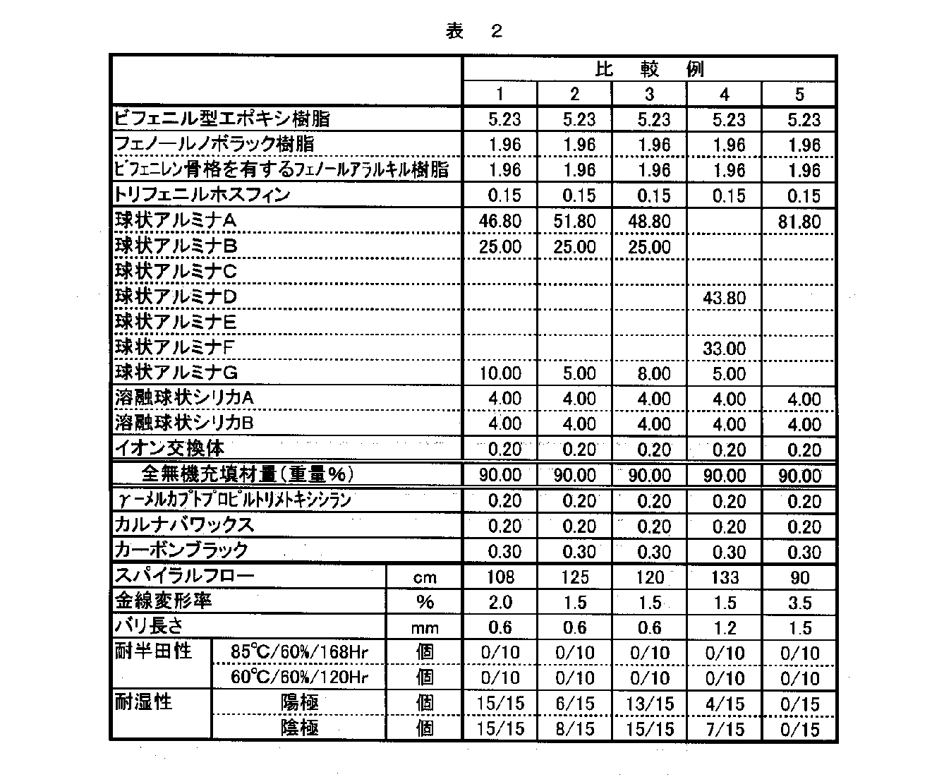
実施例2〜8、比較例1〜5
表1、表2の配合に従い、実施例1と同様にしてエポキシ樹脂組成物を得、同様に評価した。これらの評価結果を表1、表2に示す。
実施例1以外で用いたアルミナを以下に示す。
アルミナC(平均粒径55.0μm、比表面積0.1m2/g、極大点粒径55μm、α構造含有率95重量%)
アルミナD(平均粒径38.0μm、比表面積0.1m2/g、極大点粒径38μm、α構造含有率95重量%)
アルミナE(平均粒径33.0μm、比表面積0.3m2/g、極大点粒径33μm、α構造含有率95重量%)
アルミナF(平均粒径3.0μm、比表面積0.8m2/g、極大点粒径3μm、α構造含有率30重量%)
アルミナG(平均粒径0.6μm、比表面積8.1m2/g、極大点粒径0.6μm、α構造含有率1重量%)
Examples 2-8, Comparative Examples 1-5
According to the composition of Table 1 and Table 2, an epoxy resin composition was obtained in the same manner as in Example 1 and evaluated in the same manner. These evaluation results are shown in Tables 1 and 2.
Alumina used in other than Example 1 is shown below.
Alumina C (average particle size 55.0 μm, specific surface area 0.1 m 2 / g, maximum point particle size 55 μm, α structure content 95% by weight)
Alumina D (average particle size 38.0 μm, specific surface area 0.1 m 2 / g, maximum point particle size 38 μm, α structure content 95% by weight)
Alumina E (average particle size 33.0 μm, specific surface area 0.3 m 2 / g, maximum point particle size 33 μm, α structure content 95% by weight)
Alumina F (average particle size 3.0 μm, specific surface area 0.8 m 2 / g, maximum point particle size 3 μm, α structure content 30% by weight)
Alumina G (average particle size 0.6 μm, specific surface area 8.1 m 2 / g, maximum point particle size 0.6 μm, α structure content 1% by weight)
本発明の半導体封止用エポキシ樹脂組成物は、従来の技術では得られなかった耐湿性能を得ることが出来、なおかつアルミナを高充填することにより優れた、熱放散性、耐半田性を付与することが出来るので、表面実装用の樹脂封止型半導体装置、とりわけ無鉛半田対応用として好適に用いることができる。
The epoxy resin composition for semiconductor encapsulation of the present invention can obtain moisture resistance performance that was not obtained by the conventional technology, and imparts excellent heat dissipation and solder resistance by high filling with alumina. Therefore, it can be suitably used as a resin-sealed semiconductor device for surface mounting, particularly for lead-free solder.
Claims (8)
Priority Applications (1)
| Application Number | Priority Date | Filing Date | Title |
|---|---|---|---|
| JP2004103869A JP4525139B2 (en) | 2004-03-31 | 2004-03-31 | The manufacturing method of the epoxy resin composition for semiconductor sealing. |
Applications Claiming Priority (1)
| Application Number | Priority Date | Filing Date | Title |
|---|---|---|---|
| JP2004103869A JP4525139B2 (en) | 2004-03-31 | 2004-03-31 | The manufacturing method of the epoxy resin composition for semiconductor sealing. |
Publications (2)
| Publication Number | Publication Date |
|---|---|
| JP2005290076A true JP2005290076A (en) | 2005-10-20 |
| JP4525139B2 JP4525139B2 (en) | 2010-08-18 |
Family
ID=35323385
Family Applications (1)
| Application Number | Title | Priority Date | Filing Date |
|---|---|---|---|
| JP2004103869A Expired - Fee Related JP4525139B2 (en) | 2004-03-31 | 2004-03-31 | The manufacturing method of the epoxy resin composition for semiconductor sealing. |
Country Status (1)
| Country | Link |
|---|---|
| JP (1) | JP4525139B2 (en) |
Cited By (13)
| Publication number | Priority date | Publication date | Assignee | Title |
|---|---|---|---|---|
| JPWO2006011662A1 (en) * | 2004-07-29 | 2008-05-01 | 住友ベークライト株式会社 | Epoxy resin composition and semiconductor device |
| JP2008248004A (en) * | 2007-03-29 | 2008-10-16 | Admatechs Co Ltd | Inorganic powder for resin composition addition and resin composition |
| WO2013018525A1 (en) | 2011-08-04 | 2013-02-07 | 株式会社日立製作所 | Epoxy resin composition for cast molding and electrical device using same |
| WO2015060125A1 (en) | 2013-10-24 | 2015-04-30 | Dic株式会社 | Resin composition, heat-dissipating material, and heat-dissipating member |
| JP2017190425A (en) * | 2016-04-15 | 2017-10-19 | 京セラ株式会社 | Granular resin composition for semiconductor sealing and semiconductor device |
| WO2019131669A1 (en) * | 2017-12-28 | 2019-07-04 | 日立化成株式会社 | Sealing composition and semiconductor device |
| JPWO2018181601A1 (en) * | 2017-03-28 | 2020-02-06 | 日立化成株式会社 | Epoxy resin composition for sealing and electronic component device |
| WO2020193323A1 (en) * | 2019-03-27 | 2020-10-01 | Siemens Aktiengesellschaft | Casting resin, moulding material therefrom, use therefor, and electrical insulation |
| JP2021138864A (en) * | 2020-03-06 | 2021-09-16 | 住友ベークライト株式会社 | Sealing resin composition and electronic device |
| US20220098455A1 (en) * | 2020-08-19 | 2022-03-31 | Lg Chem, Ltd. | Resin composition for bonding semiconductor and adhesive film for semiconductor using the same |
| JP2023114497A (en) * | 2022-02-07 | 2023-08-18 | 信越化学工業株式会社 | Thermally conductive resin composition |
| WO2025084382A1 (en) * | 2023-10-19 | 2025-04-24 | デンカ株式会社 | Alumina powder, resin composition, and adhesive agent |
| WO2025084383A1 (en) * | 2023-10-19 | 2025-04-24 | デンカ株式会社 | Alumina powder, resin composition, and adhesive |
Families Citing this family (1)
| Publication number | Priority date | Publication date | Assignee | Title |
|---|---|---|---|---|
| CN109909494B (en) * | 2019-03-14 | 2021-05-04 | 昆山市中迪新材料技术有限公司 | High-thermal-conductivity powder and preparation method and application thereof |
Citations (7)
| Publication number | Priority date | Publication date | Assignee | Title |
|---|---|---|---|---|
| JPH0418445A (en) * | 1990-05-10 | 1992-01-22 | Shin Etsu Chem Co Ltd | Epoxy resin composition and cured product thereof |
| JPH07278415A (en) * | 1994-04-13 | 1995-10-24 | Shin Etsu Chem Co Ltd | Resin composition for semiconductor encapsulation and semiconductor device |
| JP2001019425A (en) * | 1999-07-06 | 2001-01-23 | Denki Kagaku Kogyo Kk | Spherical alumina powder and method for producing the same |
| JP2003020364A (en) * | 2001-07-05 | 2003-01-24 | Denki Kagaku Kogyo Kk | Spherical inorganic powder and resin composition filled with the same |
| JP2003110065A (en) * | 2001-10-01 | 2003-04-11 | Denki Kagaku Kogyo Kk | Spherical inorganic powder and its use |
| JP2003146648A (en) * | 2001-11-15 | 2003-05-21 | Denki Kagaku Kogyo Kk | Spherical inorganic powder and resin composition filled with the same |
| JP2004244491A (en) * | 2003-02-13 | 2004-09-02 | Denki Kagaku Kogyo Kk | High thermal conductive inorganic powder and resin composition thereof |
-
2004
- 2004-03-31 JP JP2004103869A patent/JP4525139B2/en not_active Expired - Fee Related
Patent Citations (7)
| Publication number | Priority date | Publication date | Assignee | Title |
|---|---|---|---|---|
| JPH0418445A (en) * | 1990-05-10 | 1992-01-22 | Shin Etsu Chem Co Ltd | Epoxy resin composition and cured product thereof |
| JPH07278415A (en) * | 1994-04-13 | 1995-10-24 | Shin Etsu Chem Co Ltd | Resin composition for semiconductor encapsulation and semiconductor device |
| JP2001019425A (en) * | 1999-07-06 | 2001-01-23 | Denki Kagaku Kogyo Kk | Spherical alumina powder and method for producing the same |
| JP2003020364A (en) * | 2001-07-05 | 2003-01-24 | Denki Kagaku Kogyo Kk | Spherical inorganic powder and resin composition filled with the same |
| JP2003110065A (en) * | 2001-10-01 | 2003-04-11 | Denki Kagaku Kogyo Kk | Spherical inorganic powder and its use |
| JP2003146648A (en) * | 2001-11-15 | 2003-05-21 | Denki Kagaku Kogyo Kk | Spherical inorganic powder and resin composition filled with the same |
| JP2004244491A (en) * | 2003-02-13 | 2004-09-02 | Denki Kagaku Kogyo Kk | High thermal conductive inorganic powder and resin composition thereof |
Cited By (31)
| Publication number | Priority date | Publication date | Assignee | Title |
|---|---|---|---|---|
| JPWO2006011662A1 (en) * | 2004-07-29 | 2008-05-01 | 住友ベークライト株式会社 | Epoxy resin composition and semiconductor device |
| JP5019251B2 (en) * | 2004-07-29 | 2012-09-05 | 住友ベークライト株式会社 | Epoxy resin composition and semiconductor device |
| JP2008248004A (en) * | 2007-03-29 | 2008-10-16 | Admatechs Co Ltd | Inorganic powder for resin composition addition and resin composition |
| WO2013018525A1 (en) | 2011-08-04 | 2013-02-07 | 株式会社日立製作所 | Epoxy resin composition for cast molding and electrical device using same |
| CN103717669A (en) * | 2011-08-04 | 2014-04-09 | 株式会社日立制作所 | Epoxy resin composition for injection molding and electric appliance using same |
| WO2015060125A1 (en) | 2013-10-24 | 2015-04-30 | Dic株式会社 | Resin composition, heat-dissipating material, and heat-dissipating member |
| KR20160078340A (en) | 2013-10-24 | 2016-07-04 | 디아이씨 가부시끼가이샤 | Resin composition, heat-dissipating material, and heat-dissipating member |
| US10113096B2 (en) | 2013-10-24 | 2018-10-30 | Dic Corporation | Resin composition, heat-dissipating material, and heat-dissipating member |
| JP2017190425A (en) * | 2016-04-15 | 2017-10-19 | 京セラ株式会社 | Granular resin composition for semiconductor sealing and semiconductor device |
| JP7443768B2 (en) | 2017-03-28 | 2024-03-06 | 株式会社レゾナック | Epoxy resin composition for sealing and electronic component devices |
| JPWO2018181601A1 (en) * | 2017-03-28 | 2020-02-06 | 日立化成株式会社 | Epoxy resin composition for sealing and electronic component device |
| JPWO2019131669A1 (en) * | 2017-12-28 | 2020-12-24 | 昭和電工マテリアルズ株式会社 | Encapsulation composition and semiconductor device |
| CN111566163B (en) * | 2017-12-28 | 2024-02-13 | 株式会社力森诺科 | Sealing compositions and semiconductor devices |
| KR102815688B1 (en) | 2017-12-28 | 2025-06-04 | 가부시끼가이샤 레조낙 | Sealing composition and semiconductor device |
| CN111566163A (en) * | 2017-12-28 | 2020-08-21 | 日立化成株式会社 | Sealing composition and semiconductor device |
| JP7571810B2 (en) | 2017-12-28 | 2024-10-23 | 株式会社レゾナック | Encapsulating composition and semiconductor device |
| KR20200103682A (en) * | 2017-12-28 | 2020-09-02 | 히타치가세이가부시끼가이샤 | Sealing composition and semiconductor device |
| WO2019131669A1 (en) * | 2017-12-28 | 2019-07-04 | 日立化成株式会社 | Sealing composition and semiconductor device |
| JP7238791B2 (en) | 2017-12-28 | 2023-03-14 | 株式会社レゾナック | Encapsulating composition and semiconductor device |
| TWI797222B (en) * | 2017-12-28 | 2023-04-01 | 日商日立化成股份有限公司 | Sealing composition and semiconductor device |
| JP2023067951A (en) * | 2017-12-28 | 2023-05-16 | 株式会社レゾナック | Encapsulating composition and semiconductor device |
| CN113906524A (en) * | 2019-03-27 | 2022-01-07 | 西门子股份公司 | Casting resin, molding material made of the same, use thereof and electrical insulation |
| CN113906524B (en) * | 2019-03-27 | 2024-09-20 | 西门子股份公司 | Casting resins, molding materials made therefrom, their use and electrical insulation |
| WO2020193323A1 (en) * | 2019-03-27 | 2020-10-01 | Siemens Aktiengesellschaft | Casting resin, moulding material therefrom, use therefor, and electrical insulation |
| JP2021138864A (en) * | 2020-03-06 | 2021-09-16 | 住友ベークライト株式会社 | Sealing resin composition and electronic device |
| US20220098455A1 (en) * | 2020-08-19 | 2022-03-31 | Lg Chem, Ltd. | Resin composition for bonding semiconductor and adhesive film for semiconductor using the same |
| US11939494B2 (en) * | 2020-08-19 | 2024-03-26 | Lg Chem, Ltd. | Resin composition for bonding semiconductor and adhesive film for semiconductor using the same |
| JP2023114497A (en) * | 2022-02-07 | 2023-08-18 | 信越化学工業株式会社 | Thermally conductive resin composition |
| US12565608B2 (en) | 2022-02-07 | 2026-03-03 | Shin-Etsu Chemical Co., Ltd. | Thermally conductive resin composition |
| WO2025084382A1 (en) * | 2023-10-19 | 2025-04-24 | デンカ株式会社 | Alumina powder, resin composition, and adhesive agent |
| WO2025084383A1 (en) * | 2023-10-19 | 2025-04-24 | デンカ株式会社 | Alumina powder, resin composition, and adhesive |
Also Published As
| Publication number | Publication date |
|---|---|
| JP4525139B2 (en) | 2010-08-18 |
Similar Documents
| Publication | Publication Date | Title |
|---|---|---|
| JP4525139B2 (en) | The manufacturing method of the epoxy resin composition for semiconductor sealing. | |
| JP4496786B2 (en) | Epoxy resin composition and semiconductor device | |
| JP4973322B2 (en) | Epoxy resin composition and semiconductor device | |
| WO2006059542A1 (en) | Epoxy resin composition and semiconductor devices | |
| JP4736432B2 (en) | Epoxy resin composition and semiconductor device | |
| JP5407767B2 (en) | Epoxy resin composition and semiconductor device | |
| JP2004292514A (en) | Epoxy resin composition and semiconductor device | |
| JP4631296B2 (en) | Epoxy resin composition and semiconductor device | |
| JP4525141B2 (en) | Method for producing epoxy resin composition for semiconductor encapsulation and method for producing epoxy resin composition for area mounting type semiconductor encapsulation | |
| JP5098125B2 (en) | Epoxy resin composition and semiconductor device | |
| JP2003213084A (en) | Epoxy resin composition and semiconductor device | |
| JP5067994B2 (en) | Epoxy resin composition and semiconductor device | |
| JP2006104393A (en) | Epoxy resin composition and semiconductor device | |
| JP2005146141A (en) | Resin composition for sealing and resin sealing type semiconductor device | |
| JP2006022188A (en) | Epoxy resin composition, method for producing the same, and semiconductor device | |
| JP2006257309A (en) | Epoxy resin composition for sealing semiconductor and semiconductor device | |
| JP3986917B2 (en) | Epoxy resin composition and semiconductor device | |
| JP2007231252A (en) | Epoxy resin composition for semiconductor encapsulation and semiconductor device sealed with the composition | |
| JP4687195B2 (en) | Epoxy resin composition for semiconductor encapsulation and semiconductor device | |
| JP2003292569A (en) | Epoxy resin composition and semiconductor device | |
| JP5055778B2 (en) | Epoxy resin composition, epoxy resin molding material and semiconductor device | |
| JP2005139260A (en) | Epoxy resin composition and semiconductor device | |
| JP2001253999A (en) | Epoxy resin molding material and semiconductor device | |
| JP2003238660A (en) | Epoxy resin composition and semiconductor device | |
| JP2002317102A (en) | Epoxy resin composition and semiconductor device |
Legal Events
| Date | Code | Title | Description |
|---|---|---|---|
| A621 | Written request for application examination |
Free format text: JAPANESE INTERMEDIATE CODE: A621 Effective date: 20070112 |
|
| A131 | Notification of reasons for refusal |
Free format text: JAPANESE INTERMEDIATE CODE: A131 Effective date: 20090901 |
|
| A521 | Request for written amendment filed |
Free format text: JAPANESE INTERMEDIATE CODE: A523 Effective date: 20091027 |
|
| A131 | Notification of reasons for refusal |
Free format text: JAPANESE INTERMEDIATE CODE: A131 Effective date: 20100112 |
|
| A521 | Request for written amendment filed |
Free format text: JAPANESE INTERMEDIATE CODE: A523 Effective date: 20100310 |
|
| TRDD | Decision of grant or rejection written | ||
| A01 | Written decision to grant a patent or to grant a registration (utility model) |
Free format text: JAPANESE INTERMEDIATE CODE: A01 Effective date: 20100511 |
|
| A01 | Written decision to grant a patent or to grant a registration (utility model) |
Free format text: JAPANESE INTERMEDIATE CODE: A01 |
|
| A61 | First payment of annual fees (during grant procedure) |
Free format text: JAPANESE INTERMEDIATE CODE: A61 Effective date: 20100524 |
|
| FPAY | Renewal fee payment (event date is renewal date of database) |
Free format text: PAYMENT UNTIL: 20130611 Year of fee payment: 3 |
|
| R150 | Certificate of patent or registration of utility model |
Ref document number: 4525139 Country of ref document: JP Free format text: JAPANESE INTERMEDIATE CODE: R150 Free format text: JAPANESE INTERMEDIATE CODE: R150 |
|
| FPAY | Renewal fee payment (event date is renewal date of database) |
Free format text: PAYMENT UNTIL: 20130611 Year of fee payment: 3 |
|
| FPAY | Renewal fee payment (event date is renewal date of database) |
Free format text: PAYMENT UNTIL: 20140611 Year of fee payment: 4 |
|
| LAPS | Cancellation because of no payment of annual fees |