EP4557906A2 - Verfahren zum lesen eines dreidimensionalen flash-speichers - Google Patents
Verfahren zum lesen eines dreidimensionalen flash-speichers Download PDFInfo
- Publication number
- EP4557906A2 EP4557906A2 EP25167197.0A EP25167197A EP4557906A2 EP 4557906 A2 EP4557906 A2 EP 4557906A2 EP 25167197 A EP25167197 A EP 25167197A EP 4557906 A2 EP4557906 A2 EP 4557906A2
- Authority
- EP
- European Patent Office
- Prior art keywords
- voltage
- select gate
- unsel
- applying
- prepare
- Prior art date
- Legal status (The legal status is an assumption and is not a legal conclusion. Google has not performed a legal analysis and makes no representation as to the accuracy of the status listed.)
- Pending
Links
Images


Classifications
-
- G—PHYSICS
- G11—INFORMATION STORAGE
- G11C—STATIC STORES
- G11C11/00—Digital stores characterised by the use of particular electric or magnetic storage elements; Storage elements therefor
- G11C11/56—Digital stores characterised by the use of particular electric or magnetic storage elements; Storage elements therefor using storage elements with more than two stable states represented by steps, e.g. of voltage, current, phase, frequency
- G11C11/5671—Digital stores characterised by the use of particular electric or magnetic storage elements; Storage elements therefor using storage elements with more than two stable states represented by steps, e.g. of voltage, current, phase, frequency using charge trapping in an insulator
-
- G—PHYSICS
- G11—INFORMATION STORAGE
- G11C—STATIC STORES
- G11C16/00—Erasable programmable read-only memories
- G11C16/02—Erasable programmable read-only memories electrically programmable
- G11C16/04—Erasable programmable read-only memories electrically programmable using variable threshold transistors, e.g. FAMOS
- G11C16/0483—Erasable programmable read-only memories electrically programmable using variable threshold transistors, e.g. FAMOS comprising cells having several storage transistors connected in series
-
- G—PHYSICS
- G11—INFORMATION STORAGE
- G11C—STATIC STORES
- G11C16/00—Erasable programmable read-only memories
- G11C16/02—Erasable programmable read-only memories electrically programmable
- G11C16/06—Auxiliary circuits, e.g. for writing into memory
- G11C16/08—Address circuits; Decoders; Word-line control circuits
-
- G—PHYSICS
- G11—INFORMATION STORAGE
- G11C—STATIC STORES
- G11C16/00—Erasable programmable read-only memories
- G11C16/02—Erasable programmable read-only memories electrically programmable
- G11C16/06—Auxiliary circuits, e.g. for writing into memory
- G11C16/26—Sensing or reading circuits; Data output circuits
-
- G—PHYSICS
- G11—INFORMATION STORAGE
- G11C—STATIC STORES
- G11C16/00—Erasable programmable read-only memories
- G11C16/02—Erasable programmable read-only memories electrically programmable
- G11C16/06—Auxiliary circuits, e.g. for writing into memory
- G11C16/32—Timing circuits
-
- G—PHYSICS
- G11—INFORMATION STORAGE
- G11C—STATIC STORES
- G11C16/00—Erasable programmable read-only memories
- G11C16/02—Erasable programmable read-only memories electrically programmable
- G11C16/06—Auxiliary circuits, e.g. for writing into memory
- G11C16/34—Determination of programming status, e.g. threshold voltage, overprogramming or underprogramming, retention
- G11C16/3418—Disturbance prevention or evaluation; Refreshing of disturbed memory data
- G11C16/3427—Circuits or methods to prevent or reduce disturbance of the state of a memory cell when neighbouring cells are read or written
-
- G—PHYSICS
- G11—INFORMATION STORAGE
- G11C—STATIC STORES
- G11C16/00—Erasable programmable read-only memories
- G11C16/02—Erasable programmable read-only memories electrically programmable
- G11C16/06—Auxiliary circuits, e.g. for writing into memory
- G11C16/34—Determination of programming status, e.g. threshold voltage, overprogramming or underprogramming, retention
- G11C16/3436—Arrangements for verifying correct programming or erasure
- G11C16/3454—Arrangements for verifying correct programming or for detecting overprogrammed cells
- G11C16/3459—Circuits or methods to verify correct programming of nonvolatile memory cells
-
- H—ELECTRICITY
- H10—SEMICONDUCTOR DEVICES; ELECTRIC SOLID-STATE DEVICES NOT OTHERWISE PROVIDED FOR
- H10B—ELECTRONIC MEMORY DEVICES
- H10B41/00—Electrically erasable-and-programmable ROM [EEPROM] devices comprising floating gates
- H10B41/10—Electrically erasable-and-programmable ROM [EEPROM] devices comprising floating gates characterised by the top-view layout
-
- H—ELECTRICITY
- H10—SEMICONDUCTOR DEVICES; ELECTRIC SOLID-STATE DEVICES NOT OTHERWISE PROVIDED FOR
- H10B—ELECTRONIC MEMORY DEVICES
- H10B41/00—Electrically erasable-and-programmable ROM [EEPROM] devices comprising floating gates
- H10B41/20—Electrically erasable-and-programmable ROM [EEPROM] devices comprising floating gates characterised by three-dimensional arrangements, e.g. with cells on different height levels
- H10B41/23—Electrically erasable-and-programmable ROM [EEPROM] devices comprising floating gates characterised by three-dimensional arrangements, e.g. with cells on different height levels with source and drain on different levels, e.g. with sloping channels
- H10B41/27—Electrically erasable-and-programmable ROM [EEPROM] devices comprising floating gates characterised by three-dimensional arrangements, e.g. with cells on different height levels with source and drain on different levels, e.g. with sloping channels the channels comprising vertical portions, e.g. U-shaped channels
-
- H—ELECTRICITY
- H10—SEMICONDUCTOR DEVICES; ELECTRIC SOLID-STATE DEVICES NOT OTHERWISE PROVIDED FOR
- H10B—ELECTRONIC MEMORY DEVICES
- H10B43/00—EEPROM devices comprising charge-trapping gate insulators
- H10B43/10—EEPROM devices comprising charge-trapping gate insulators characterised by the top-view layout
-
- H—ELECTRICITY
- H10—SEMICONDUCTOR DEVICES; ELECTRIC SOLID-STATE DEVICES NOT OTHERWISE PROVIDED FOR
- H10B—ELECTRONIC MEMORY DEVICES
- H10B43/00—EEPROM devices comprising charge-trapping gate insulators
- H10B43/20—EEPROM devices comprising charge-trapping gate insulators characterised by three-dimensional arrangements, e.g. with cells on different height levels
- H10B43/23—EEPROM devices comprising charge-trapping gate insulators characterised by three-dimensional arrangements, e.g. with cells on different height levels with source and drain on different levels, e.g. with sloping channels
- H10B43/27—EEPROM devices comprising charge-trapping gate insulators characterised by three-dimensional arrangements, e.g. with cells on different height levels with source and drain on different levels, e.g. with sloping channels the channels comprising vertical portions, e.g. U-shaped channels
-
- G—PHYSICS
- G11—INFORMATION STORAGE
- G11C—STATIC STORES
- G11C2211/00—Indexing scheme relating to digital stores characterized by the use of particular electric or magnetic storage elements; Storage elements therefor
- G11C2211/56—Indexing scheme relating to G11C11/56 and sub-groups for features not covered by these groups
- G11C2211/562—Multilevel memory programming aspects
- G11C2211/5621—Multilevel programming verification
Definitions
- the present disclosure generally relates to the field of semiconductor technology, and more particularly, to a method for reading a three-dimensional (3D) memory.
- a three-dimensional (3D) memory architecture can address the density and performance limitation in planar memory cells.
- memory cells can be programmed for data storage based on charge-trapping technology.
- the storage information of a memory cell depends on the amount of charge trapped in a storage layer.
- fast charges i.e., charges trapped in shallow traps
- the threshold voltage determining the stored information can be different between write and read operations.
- a read-prepare step is included in a read-verification operation after programming to remove the fast charges and verify the threshold voltage of the memory cell.
- Fast charge loss depending on the intrinsic de-trapping process in the storage layer can be long, making the read-verification operation inefficient. Therefore, a need exists for a method to accelerate fast charge loss so that threshold voltage or storage information of the memory cell can be verified or read more accurately and efficiently.
- Embodiments of a method for conducting read-verification operation of a memory cell in a three-dimensional (3D) memory device is described in the present disclosure.
- One aspect of the present disclosure provides a method for conducting a read-verification operation on a target memory cell in a three-dimensional (3D) memory device.
- the method includes removing fast charges of the target memory cell at a read-prepare step, which includes applying a prepare voltage (V prepare ) on an unselected top select gate (Unsel_TSG) of an unselected memory string, applying a first off voltage (V off ) on a selected word line (Sel_WL) associated with the target memory cell, and applying a pass voltage (V pass ) on an unselected word line (Unsel_WL).
- the method also includes measuring a threshold voltage of the target memory cell at a sensing step.
- the method further includes applying a top select gate voltage (V tsg ) on a selected top select gate (Sel_TSG) of a selected memory string containing the target memory cell, and applying a lower select gate voltage (V lsg ) on a lower select gate (LSG) of the selected memory string containing the target memory cell.
- V tsg top select gate voltage
- V lsg lower select gate voltage
- applying the top select gate voltage (V tsg ) includes electrically connecting the selected memory string to a bit line.
- applying the lower select gate voltage (V lsg ) includes electrically connecting the selected memory string to an array common source.
- applying the top select gate voltage (V tsg ) includes applying a voltage between 4V to 7V. In some embodiments, applying the lower select gate voltage (V lsg ) includes applying a voltage between 4V to 7V.
- applying the pass voltage (V pass ) includes applying the pass voltage with a delay period after the selected top select gate (Sel_TSG) and the lower select gate (LSG) are at the top select gate voltage (V tsg ) and the lower select gate voltage (V lsg ), respectively.
- measuring the threshold voltage includes applying a read voltage (V read ) on the selected word line (Sel_WL). In some embodiments, applying the read voltage (V read ) includes applying a voltage between 0 to 2V. In some embodiments, applying the read voltage (V read ) includes applying a second off voltage on the unselected word line (Unsel_WL). In some embodiments, applying the second off voltage on the unselected word line (Unsel_WL) includes applying a 0V.
- applying the read voltage (V read ) includes applying the read voltage (V read ) when a voltage of the unselected top select gate (Unsel_TSG) is higher than a threshold voltage of an unselected memory cell. In some embodiments, applying the read voltage (V read ) includes applying the read voltage (V read ) when a voltage of the unselected top select gate (Unsel_TSG) equals to a threshold voltage of an unselected memory cell. In some embodiments, applying the read voltage (V read ) includes applying the read voltage (V read ) when a voltage of the unselected top select gate (Unsel_TSG) is lower than a threshold voltage of an unselected memory cell.
- applying the prepare voltage (V prepare ) includes applying a voltage between 4V to 7V.
- applying the first off voltage (V off ) includes applying a 0V.
- applying the pass voltage (V pass ) includes applying a voltage between 5V to 9V.
- removing the fast charges includes removing the fast charges from a storage layer of the target memory cell of a selected memory string, wherein the selected memory string includes a channel hole penetrating vertically through a film stack of alternating conductive and dielectric layers, a core filling film in a center of the channel hole, and a memory film covering a sidewall of the channel hole.
- the selected memory string also includes a channel layer sandwiched between the memory film and the core filling film.
- the memory film includes a barrier layer, the storage layer and a tunneling layer.
- removing the fast charges includes removing electrical charges from shallow traps in the storage layer of the target memory cell.
- removing the fast charges includes removing the fast charges from the target memory cell to a neighboring unselected memory cell.
- spatially relative terms such as “beneath,” “below,” “lower,” “above,” “upper,” and the like, can be used herein for ease of description to describe one element or feature's relationship to another element(s) or feature(s) as illustrated in the figures.
- the spatially relative terms are intended to encompass different orientations of the device in use or process step in addition to the orientation depicted in the figures.
- the apparatus can be otherwise oriented (rotated 90 degrees or at other orientations) and the spatially relative descriptors used herein can likewise be interpreted accordingly.
- the region 108 of the 3D memory device 100 can include a staircase region 210 and a channel structure region 211.
- the channel structure region 211 can include an array of memory strings 212, each including a plurality of stacked memory cells.
- the staircase region 210 can include a staircase structure and an array of contact structures 214 formed on the staircase structure.
- a plurality of slit structures 216 extending in WL direction across the channel structure region 211 and the staircase region 210, can divide a memory block into multiple memory fingers 218.
- At least some slit structures 216 can function as the common source contact (e.g., array common source) for an array of memory strings 212 in channel structure regions 211.
- a top select gate cut 220 can be disposed, for example, in the middle of each memory finger 218 to divide a top select gate (TSG) of the memory finger 218 into two portions, and thereby can divide a memory finger into two memory slices 224, where memory cells in a memory slice 224 that share the same word line form a programmable (read/write) memory page. While erase operation of a 3D NAND memory can be carried out at memory block level, read and write operations can be carried out at memory page level.
- a memory page can be kilobytes (KB) in size.
- region 108 also includes dummy memory strings 222 for process variation control during fabrication and/or for additional mechanical support.
- each memory string 212 can include three memory cells 340-1, 340-2 and 340-3, corresponding to the control gates 333-1, 333-2 and 333-3, respectively.
- the number of control gates and the number of memory cells can be more than three to increase storage capacity.
- the memory array structure 300 can also include other structures, for example, TSG cut, common source contact (i.e., array common source) and dummy memory string. These structures are not shown in Fig. 3 for simplicity.
- Fig. 4(a) illustrates a schematic cross-section of a 3D NAND memory 400a, which includes memory cells similar to the memory cell 340 in Fig. 3 .
- the memory cell 340-3 includes a control gate (e.g., the control gate 333), a memory film (e.g., the memory film 337) and a channel layer (e.g., the channel layer 338, also referred to as the channel).
- the memory film 337 can be disposed on a sidewall of each channel hole 336 (illustrated in Fig. 3 ).
- the memory film 337 can include a barrier layer 422, a storage layer 424, and a tunneling layer 426.
- the barrier layer 422 can be used to block the movement of electronic charges 428 between the control gate 333 and the storage layer 424.
- the barrier layer 422 can include silicon oxide and high dielectric constant (high-k) dielectrics, for example, aluminum oxide.
- the storage layer 424 can be used to store electronic charges 428 and can include silicon nitride. The storage and/or removal of charges in the storage layer 424 can impact the on/off state and/or a conductance of the channel layer 338.
- the tunneling layer 426 can be used to control the tunneling of electronic charges 428 (electrons or holes) between the channel layer 338 and the storage layer 424.
- the tunneling layer 426 can be silicon oxide, silicon nitride, silicon oxynitride, or any combination thereof.
- the channel layer 338 can be disposed on a sidewall of the memory film 337 in the channel hole 336 (in Fig. 3 .)
- the channel layer 338 can include amorphous silicon, polycrystalline silicon, and/or monocrystalline silicon.
- Fig. 4(b) shows a schematic circuit diagram of a 3D memory array 400b.
- the 3D memory array 400b includes a plurality of memory strings 212, each memory string 212 having a plurality of stacked memory cells 340.
- the memory string 212 also includes at least one field effect transistor (e.g., MOSFET) at each end, which is controlled by the lower select gate (LSG) 332 and the top select gate (TSG) 334, respectively. And the two respective transistors are referred to as lower and top select transistors 332-T and 334-T.
- the stacked memory cells 340 can be controlled by the control gates 333, where the control gates 333 are connected to word lines (not shown) of the 3D memory array 400b.
- the drain terminal of the top select transistor 334-T can be connected to the bit lines (e.g., the bit line 341-1, 341-2, 341-3, etc.), and the source terminal of the lower select transistor 332-T can be connected to the doped source line region 344 ( see Fig. 3 ), from where an array common source (ACS) 446 can be formed.
- the array common source 446 can be shared by the memory strings 212 in an entire memory block, and is also referred to as the common source line.
- a NAND memory in a NAND memory, read and write operations can be performed in a memory page, for example memory page 448, which includes memory cells sharing the same word line.
- each memory cell can be in an erased state or a programmed state. Initially, all memory cells in a block can be reset to the erased state as logic "1" by applying, for example, a negative voltage between the control gates 333 and source terminals of the memory cells (e.g., the array common source 446) such that all the electronic charges 428 in the storage layers 424 of the memory cells can be removed.
- the threshold voltage V th of the memory cells 340 can be reset to the lowest value, and the corresponding current flowing through the memory cells 340 between the source terminal (e.g., the array common source 446) and the drain terminal (e.g., the bit lines 341) can be at the highest level for a given bias on the word lines.
- a high positive voltage pulse (e.g., 12V to 18V) can be applied on the control gate 333 such that electronic charges 428 (e.g., electrons) can be injected into the storage layer 424 of the memory cell 340, where the electronic charges 428-1 and 428-2 can be randomly captured by deep and shallow traps, respectively.
- the threshold voltage V th of the memory cell 340 can be raised to a higher value than that of the erased state. At a higher threshold voltage V th , the current flowing through the source and drain terminals of the memory cell can be at a reduced level for a given bias on the word lines. By measuring (i.e., reading) the memory cell current, the threshold voltage V th and thereby the state of the memory cell 340 can be determined accordingly.
- each memory cell 340 can have multiple programed states, i.e., multiple values of threshold voltages V th . After every programming pulse, a read-verification operation can be performed to check the state of the memory cell. As such, each memory cell 340 can store multiple bits, leading to significant increase of storage capacity.
- the programmed state immediately after writing cannot reflect the target threshold voltage V th of the memory cell 340 in real applications. Applying the fake high threshold voltage V th can cause high bit-error-rate in the memory. Therefore, it is necessary to de-trap and remove fast charges prior to read operation such that the V th distribution profile of each programmed state can be more accurately determined.
- Fig. 5 illustrates a timing diagram of a read-verification operation 500 with a prepare voltage (pre-pulse) applied on a selected word line, according to some embodiments of the present disclosure.
- the read-verification operation 500 can reduce read disturb for unselected memory strings in a 3D NAND memory. Read disturb can occur when the threshold voltage V th (i.e., the programmed state) of an unselected memory cell is changed or disturbed during read or read-verification of a selected memory cell.
- the read-verification operation 500 includes two steps, i.e., a read-prepare step and a sensing step, having duration of t prepare and t sensing , respectively.
- a selected top select gate (Sel_TSG), unselected top select gates (Unsel_TSG), a selected word line (Sel_WL), unselected word lines (Unsel_WL) and the lower select gate (LSG) are shown in Fig. 5 .
- the read-verification operation 500 starts with the read-prepare step.
- the TSG 334 and the LSG 332 of a selected memory string for example TSG 334-3 and LSG 332-3 of a selected memory string 212-3 in Fig. 4(b) , can be applied with a top select gate voltage V tsg and a lower select gate voltage V lsg .
- a corresponding top select transistor 334-T and a lower select transistor 332-T of the selected memory string 212-3 can be switched on.
- the top and lower select gate voltages V tsg and V lsg can be in a range between 4V to 7V. Accordingly, a current path through the stacked memory cells 340 can be established for the selected memory string 212-3. For example, the current flowing through the selected memory string 212-3 can be detected from the bit line 341-3 and the array common source 446 that are electrically connected with the selected memory string 212-3.
- the TSG of unselected memory strings (Unsel-TSG), for example TSG 334-1 of memory string 212-1 in Fig. 4(b) , can be applied with a first off voltage (V off ), for example 0V, to switch off a corresponding top select transistor 334-T.
- V off first off voltage
- Current path between the unselected memory strings 212-1 and bit lines 341-1 can be disconnected. Therefore, the channel of selected memory string 212-3 and unselected memory strings 212-1 can be electrically isolated.
- a selected word line (e.g., Sel_WL in Fig. 4(b) ) can be applied with a prepare voltage V prepare (also referred to as pre-pulse), while other word lines not selected (e.g., Unsel_WL in Fig. 4(b) ) can be applied with a pass voltage V pass .
- the selected word line are electrically connected to the control gate 333 of the target memory cell 340-3.
- the prepare voltage V prepare can be in a range between 4V to 7V, and the pass voltage V pass can be in a range between 5V to 9V.
- the pass voltage V pass can be higher than the highest threshold voltage of the programmed states such that the memory cells on the selected memory string 212-3 can be fully switched on.
- the prepare voltage V prepare is applied on the selected word line Sel_WL
- the target memory cell 340-3 can also be switched on. Therefore, at time t 1 , the top and lower select transistors 334-T and 332-T, and all memory cells 340 of the selected memory string 212-3 are switched on.
- de-trapped fast charges 428-2 from the storage layer 424 can be removed through the conductive path.
- fast charge loss can be a slow process, which is shown in the timing diagram of the selected word line (Sel_WL) in Fig. 5 .
- fast charges 428-2 can also be removed by thermal annealing or by implementing soft erase with a low negative voltage on the control gate.
- the read-prepare step generally can take a long time and thus impact the efficiency of the read-verification operation. Therefore, a need exists for a read-verification operation to provide accelerated fast charge loss and shorten read-prepare step.
- the read-prepare step can reduce read disturb for the unselected memory strings, for example, memory strings 212-1 and 212-2 in Fig. 4(b) .
- the unselected top select gates (Unsel_TSG) for unselected memory strings e.g., TSG 334-1 of memory string 212-1
- V off the first off voltage
- bit lines e.g., bit line 341-1
- the lower select gates (LSG) of the unselected memory strings are applied with the lower select gate voltage V lsg such that the lower select transistors 332-T are switched on.
- the prepare voltage V prepare on the selected word line (Sel_WL)
- corresponding memory cells e.g., memory cells 340-1, 340-2, 340-3, etc.
- the channel of the memory cells of the unselected memory strings can be electrically connected to the array common source 446 to maintain at a predetermined potential, e . g ., ground.
- the memory cells corresponding to the selected word line may not be fully switched on (e.g., a voltage applied on the selected word line is lower than the threshold voltage V th of the memory cell 340-1).
- Upper memory cells i.e., memory cells located between the bit line (e.g., bit line 341-1) and the selected word line (Sel_WL) of the unselected memory string (e.g., memory string 212-1), can have floating channels, where the channel layer is not electrically connected to the bit lines 341 or the common array source 446.
- Channel potential of the upper memory cells of the unselected memory string can vary randomly. Memory cells with floating channel can suffer charge loss due to an unknown electrical field between the control gate 333 and the channel layer 338 ( see FIG. 4(a) ). The trapped charges 428 and thereby the threshold voltages V th (i.e., programmed states) of the memory cells can be changed or disturbed, where the change can be significant with the increased number of reading operation. By introducing the read_prepare step prior to the sensing step, as described previously, read disturb on the unselected memory strings can be reduced.
- the voltage bias on the selected word line can be reduced from the prepare voltage V prepare to a read voltage V read to sense (i.e., read or measure) the threshold voltage V th of the target memory cell.
- the read voltage V read can be in a range between 0V to 2V.
- the target memory cell can be switch on and form a conductive path in the channel layer 338. If the threshold voltage V th is higher than the read voltage V read , the channel of the target memory cell is switched off. The programmed state of the target memory cell can be determined accordingly.
- the transition period from the prepare voltage V prepare to the read voltage V read is a slow process due to parasitic capacitance and resistance as well as slow de-trapping process of fast trap loss.
- the sensing step can start after the Sel_WL reach the read voltage V read , which increases the overall duration t prepare of read-prepare step.
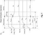
- Fig. 6 illustrates a read-verification operation 600 designed to accelerate fast charge loss in a three-dimensional flash memory, according to some embodiments of the present disclosure.
- the read-verification operation 600 also includes the read-prepare step and the sensing step.
- the Sel_TSG and the LSG can be applied with the top and lower select gate voltages V tsg and V lsg , respectively, to switch on the top and lower select transistors 334-T and 332-T (in Fig. 4(b) ), similar to those used in the read-verification operation 500 in Fig. 5 .
- the Unsel_TSG of the read-verification operation 600 is applied with the prepare voltage V prepare during the read-prepare step. Accordingly, the selected and unselected memory strings can all be electrically accessed from the bit line 341 and the array common source 446.
- the selected memory cell can be switched off by applying a second off voltage, e.g., 0V on the selected WL (i.e., Sel_WL).
- the unselected memory cells i.e., Unsel_WL
- the unselected memory cells can be switched on with the pass voltage V pass after a delay period t delay1 .
- all select transistors controlled by Sel_TSG, Unsel_TSG and LSG are turned on with applied voltages V tsg , V prepare and V lsg and thus the channel of the memory string 212 can be electrically connected to the bit line 341 and the array common source 446 (shown in Fig.
- the channel of the selected memory cell can be electrically connected to the bit line 341 through upper memory cells and to the array common source 446 through the lower memory cells. The channel of the selected memory cell can thereby be held at a potential adjustable by the voltage of the bit line 341 and the array common source 446.
- the delay period t delay1 is implemented such that the channel of the memory string 212 is not electrically isolated from the bit line 341 or the array common source 446 before Unsel_WL can be ramped up from 0V to the pass voltage V pass .
- the top select transistors are off and upper portion of the channel layer 338 that is located close to the bit line 341 becomes a floating node. More specifically upper memory cells located between the bit line and the selected memory cell can have a floating channel potential.
- lower portion of the channel layer 338 that is located close to the array common source 446 becomes a floating node.
- More specifically lower memory cells located between the bit line and the selected memory cell can have a floating channel potential.
- channel potential of the memory cells can be boosted by the pass voltage V pass of the Unsel_WL through coupled capacitance.
- the boosted channel potential of the unselected memory cells can influence the channel potential of the neighboring selected memory cell and influence fast charge removing process.
- the neighboring unselected memory cells 340 are switched on.
- an electric field parallel to the channel can be established accordingly.
- the electric field between the neighboring selected and unselected word line can also extend into the charge storage layer 424, the tunneling layer 426 and the channel layer 338.
- the electric field can generate an electric force on the fast charges 428-2 captured in the storage layer 424. The electric force can de-trap the fast charges 428-2 from the shallow traps, pull them towards the neighboring unselected memory cells.
- fast charges 428-2 in the storage layer 424 of the selected memory cell 340-3 can be removed through electric field from neighboring unselected memory cells.
- the duration of the read-prepare step of the read-verification operation 600 includes the sum of the delay period t delay1 and t delay2 . Both t delay1 and t delay2 can be pre-determined values.
- the read voltage V read is applied on the Sel_WL to start the sensing step and BL pre-charge.
- the sensing step has a duration of t sensing , which can also be a predetermined value.
- a voltage of 0V is applied on the Unsel_TSG, which switches off the unselected top select gates and electrically isolates the channel of selected memory string from the channel of unselected memory strings. Similar to the read-verification operation 500 (in Fig. 5 ), the ramping-down process from the prepare voltage V prepare to 0V has a delay time, resulting from parasitic resistance and capacitance of the 3D memory structure.
- duration of the read-prepare step i.e., t delay1 +t delay2 is less than t prepare2 .
- the sensing step and BL pre-charge start when Unsel_TSG is above V th and the unselected top select transistor is still on. This operation can provide a minimum time used for the read-prepare step, although more power is consumed.
- the time saved t PROG-save is a difference between t prepare1 and t delay1 +t delay2 .
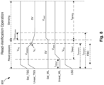
- Fig. 7 illustrates a read-verification operation 700 designed to accelerate fast charge loss in a three-dimensional flash memory, according to some embodiments of the present disclosure.
- the read-verification operation 700 is similar to the read-verification operation 600, except having a duration of the read-prepare step (i.e., t delay1 +t delay2 ) equals t prepare2 , the minimum time requirement for turning off the Unsel_TSG.
- the sensing step and BL pre-charge start when the unselected top select transistors are just turned off.
- the time saved t PROG-save can be expressed as the difference between t prepare1 and t delay1 +t delay2 , as shown in Fig. 7 . This operation can be sped-up, and thus improved, without consuming more power.
- accelerating fast charge loss in a 3D NAND flash memory can be achieved by applying the prepare voltage V prepare on Unsel_TSG, the pass voltage V pass on the Unsel_WL, and 0V on the Sel-WL at the read-prepare step.
- the threshold voltage V th of the target memory cell, associated with the Sel_WL, can be stabilized before the sensing step such that the verified storage data can be more reliable.
- the read-verification operation described above can greatly reduce the time required at the read-prepare step.
- 3D NAND flash memory with multi-level-cells typically uses an algorithm with incremental step pulses to program the memory cells. After every program pulse, a read-verification operation is performed to check the state of the memory cells. When the memory cell reaches the target state (i.e., target threshold voltage), the program will be stopped. In the meantime, the memory cells not programed to the target state are calculated towards failed bit count (FBC), where the FBC can be executed in parallel to the read-verification operation to save the time of the entire programming cycle. As shown in Figs. 6-8 , FBC operation can be performed in parallel with the read-prepare step.
- FBC failed bit count
- the present disclosure provides a method for conducting a read-verification operation on a target memory cell in a three-dimensional (3D) memory device, where the method includes removing fast charges of the target memory cell at a read-prepare step and measuring a threshold voltage of the target memory cell at a sensing step.
- Removing the fast charges of the target memory cell includes applying a prepare voltage (V prepare ) on an unselected top select gate (Unsel_TSG) of an unselected memory string, applying a first off voltage (V off ) on a selected word line (Sel_WL) associated with the target memory cell, and applying a pass voltage (V pass ) on an unselected word line (Unsel_WL).
Landscapes
- Engineering & Computer Science (AREA)
- Microelectronics & Electronic Packaging (AREA)
- Computer Hardware Design (AREA)
- Read Only Memory (AREA)
- Semiconductor Memories (AREA)
- Non-Volatile Memory (AREA)
Priority Applications (1)
| Application Number | Priority Date | Filing Date | Title |
|---|---|---|---|
| EP25167197.0A EP4557906A3 (de) | 2019-10-23 | 2019-10-23 | Verfahren zum lesen eines dreidimensionalen flash-speichers |
Applications Claiming Priority (4)
| Application Number | Priority Date | Filing Date | Title |
|---|---|---|---|
| EP19949634.0A EP3891743B1 (de) | 2019-10-23 | 2019-10-23 | Verfahren zum lesen eines dreidimensionalen flash-speichers |
| EP25167197.0A EP4557906A3 (de) | 2019-10-23 | 2019-10-23 | Verfahren zum lesen eines dreidimensionalen flash-speichers |
| PCT/CN2019/112728 WO2021077322A1 (en) | 2019-10-23 | 2019-10-23 | Method for reading three-dimensional flash memory |
| EP23181351.0A EP4236650B1 (de) | 2019-10-23 | 2019-10-23 | Verfahren zum lesen eines dreidimensionalen flash-speichers |
Related Parent Applications (3)
| Application Number | Title | Priority Date | Filing Date |
|---|---|---|---|
| EP23181351.0A Division-Into EP4236650B1 (de) | 2019-10-23 | 2019-10-23 | Verfahren zum lesen eines dreidimensionalen flash-speichers |
| EP23181351.0A Division EP4236650B1 (de) | 2019-10-23 | 2019-10-23 | Verfahren zum lesen eines dreidimensionalen flash-speichers |
| EP19949634.0A Division EP3891743B1 (de) | 2019-10-23 | 2019-10-23 | Verfahren zum lesen eines dreidimensionalen flash-speichers |
Publications (2)
| Publication Number | Publication Date |
|---|---|
| EP4557906A2 true EP4557906A2 (de) | 2025-05-21 |
| EP4557906A3 EP4557906A3 (de) | 2025-08-06 |
Family
ID=69913967
Family Applications (3)
| Application Number | Title | Priority Date | Filing Date |
|---|---|---|---|
| EP19949634.0A Active EP3891743B1 (de) | 2019-10-23 | 2019-10-23 | Verfahren zum lesen eines dreidimensionalen flash-speichers |
| EP23181351.0A Active EP4236650B1 (de) | 2019-10-23 | 2019-10-23 | Verfahren zum lesen eines dreidimensionalen flash-speichers |
| EP25167197.0A Pending EP4557906A3 (de) | 2019-10-23 | 2019-10-23 | Verfahren zum lesen eines dreidimensionalen flash-speichers |
Family Applications Before (2)
| Application Number | Title | Priority Date | Filing Date |
|---|---|---|---|
| EP19949634.0A Active EP3891743B1 (de) | 2019-10-23 | 2019-10-23 | Verfahren zum lesen eines dreidimensionalen flash-speichers |
| EP23181351.0A Active EP4236650B1 (de) | 2019-10-23 | 2019-10-23 | Verfahren zum lesen eines dreidimensionalen flash-speichers |
Country Status (7)
| Country | Link |
|---|---|
| US (4) | US11043279B2 (de) |
| EP (3) | EP3891743B1 (de) |
| JP (1) | JP7125564B2 (de) |
| KR (2) | KR20240042230A (de) |
| CN (2) | CN113223578B (de) |
| TW (1) | TWI717134B (de) |
| WO (1) | WO2021077322A1 (de) |
Families Citing this family (12)
| Publication number | Priority date | Publication date | Assignee | Title |
|---|---|---|---|---|
| EP3891743B1 (de) | 2019-10-23 | 2023-07-19 | Yangtze Memory Technologies Co., Ltd. | Verfahren zum lesen eines dreidimensionalen flash-speichers |
| KR102735053B1 (ko) * | 2020-02-21 | 2024-11-28 | 에스케이하이닉스 주식회사 | 반도체 메모리 장치 및 그 동작 방법 |
| US11264404B2 (en) | 2020-06-17 | 2022-03-01 | Micron Technology, Inc. | Microelectronic devices including a varying tier pitch, and related electronic systems and methods |
| US11398486B2 (en) | 2020-06-17 | 2022-07-26 | Micron Technology, Inc. | Microelectronic devices with tier stacks with varied tier thicknesses, and related methods and systems |
| US11340982B1 (en) * | 2020-11-02 | 2022-05-24 | Micron Technology, Inc. | Memory block defect detection and management |
| CN117423375A (zh) * | 2020-12-15 | 2024-01-19 | 长江存储科技有限责任公司 | 用于nand存储器操作的架构和方法 |
| US20220230674A1 (en) * | 2021-01-21 | 2022-07-21 | Macronix International Co., Ltd. | Read operation method for non-volatile memory device to reduce disturbance |
| CN115249508B (zh) * | 2021-09-06 | 2023-08-04 | 杭州领开半导体技术有限公司 | 改善非易失性存储器读取干扰的方法及控制系统 |
| KR102832532B1 (ko) | 2021-10-30 | 2025-07-09 | 양쯔 메모리 테크놀로지스 씨오., 엘티디. | 메모리 장치 및 그 프로그램 동작 |
| KR20230069690A (ko) | 2021-11-12 | 2023-05-19 | 삼성전자주식회사 | 반도체 메모리 소자 및 그의 제조 방법 |
| TWI812221B (zh) * | 2022-05-13 | 2023-08-11 | 旺宏電子股份有限公司 | 記憶體裝置及其操作方法 |
| US12002522B2 (en) | 2022-05-13 | 2024-06-04 | Macronix International Co., Ltd. | Memory device and operation method thereof |
Family Cites Families (54)
| Publication number | Priority date | Publication date | Assignee | Title |
|---|---|---|---|---|
| US7894269B2 (en) | 2006-07-20 | 2011-02-22 | Sandisk Corporation | Nonvolatile memory and method for compensating during programming for perturbing charges of neighboring cells |
| US8027200B2 (en) * | 2008-08-21 | 2011-09-27 | Micron Technology, Inc. | Reduction of quick charge loss effect in a memory device |
| US8737129B2 (en) * | 2008-11-14 | 2014-05-27 | Samsung Electronics Co., Ltd. | Nonvolatile memory device and read method thereof |
| KR101001449B1 (ko) | 2009-04-14 | 2010-12-14 | 주식회사 하이닉스반도체 | 불휘발성 소자의 독출 동작 방법 |
| JP2012123880A (ja) | 2010-12-10 | 2012-06-28 | Toshiba Corp | 半導体記憶装置 |
| KR20120121170A (ko) | 2011-04-26 | 2012-11-05 | 에스케이하이닉스 주식회사 | 반도체 장치 및 이의 동작 방법 |
| US8750042B2 (en) | 2011-07-28 | 2014-06-10 | Sandisk Technologies Inc. | Combined simultaneous sensing of multiple wordlines in a post-write read (PWR) and detection of NAND failures |
| WO2013075067A1 (en) * | 2011-11-18 | 2013-05-23 | Aplus Flash Technology, Inc. | Low voltage page buffer for use in nonvolatile memory design |
| WO2013095667A1 (en) * | 2011-12-23 | 2013-06-27 | Intel Corporation | Method, apparatus and system for determining access to a memory array |
| US9093369B2 (en) | 2012-06-07 | 2015-07-28 | Samsung Electronics Co., Ltd. | Three-dimensional resistive random access memory devices, methods of operating the same, and methods of fabricating the same |
| KR102102233B1 (ko) | 2013-02-22 | 2020-04-21 | 삼성전자주식회사 | 메모리 시스템 및 그것의 읽기 방법 |
| KR102160290B1 (ko) * | 2013-02-28 | 2020-09-25 | 삼성전자주식회사 | 불휘발성 메모리 및 불휘발성 메모리의 읽기 방법 |
| KR102127416B1 (ko) | 2013-06-27 | 2020-06-26 | 삼성전자주식회사 | 비휘발성 메모리 장치, 그것을 포함하는 메모리 시스템 및 그것의 읽기 방법 |
| KR20150015578A (ko) * | 2013-07-30 | 2015-02-11 | 삼성전자주식회사 | 불휘발성 메모리 장치 및 그것의 프로그램 검증 방법 |
| WO2015100434A2 (en) * | 2013-12-25 | 2015-07-02 | Aplus Flash Technology, Inc | A HYBRID NAND WITH ALL-BL m-PAGE OPERATION SCHEME |
| JP2015195070A (ja) * | 2014-03-31 | 2015-11-05 | 株式会社東芝 | 不揮発性半導体記憶装置 |
| US9165659B1 (en) | 2014-05-08 | 2015-10-20 | Sandisk Technologies Inc. | Efficient reprogramming method for tightening a threshold voltage distribution in a memory device |
| US9361993B1 (en) | 2015-01-21 | 2016-06-07 | Sandisk Technologies Inc. | Method of reducing hot electron injection type of read disturb in memory |
| US9224492B1 (en) | 2015-02-17 | 2015-12-29 | Phison Electronics Corp. | Memory management method, memory storage device and memory controlling circuit unit |
| US9899102B2 (en) | 2015-03-31 | 2018-02-20 | SK Hynix Inc. | Semiconductor device and operating method thereof |
| US20160300620A1 (en) | 2015-04-08 | 2016-10-13 | Sandisk Technologies Inc. | Multiple bit line voltage sensing for non-volatile memory |
| KR102274280B1 (ko) | 2015-06-22 | 2021-07-07 | 삼성전자주식회사 | 불휘발성 메모리 장치의 동작 방법 |
| US9627087B2 (en) * | 2015-09-11 | 2017-04-18 | Kabushiki Kaisha Toshiba | Memory device |
| US9892800B2 (en) * | 2015-09-30 | 2018-02-13 | Sunrise Memory Corporation | Multi-gate NOR flash thin-film transistor strings arranged in stacked horizontal active strips with vertical control gates |
| KR20170083346A (ko) * | 2016-01-08 | 2017-07-18 | 에스케이하이닉스 주식회사 | 반도체 메모리 장치 및 이의 동작 방법 |
| US9589978B1 (en) | 2016-02-25 | 2017-03-07 | Micron Technology, Inc. | Memory devices with stairs in a staircase coupled to tiers of memory cells and to pass transistors directly under the staircase |
| JP6581019B2 (ja) * | 2016-03-02 | 2019-09-25 | 東芝メモリ株式会社 | 半導体記憶装置 |
| US20170294367A1 (en) | 2016-04-07 | 2017-10-12 | Microchip Technology Incorporated | Flat No-Leads Package With Improved Contact Pins |
| US9607707B1 (en) * | 2016-06-30 | 2017-03-28 | Sandisk Technologies Llc | Weak erase prior to read |
| US9620233B1 (en) | 2016-06-30 | 2017-04-11 | Sandisk Technologies Llc | Word line ramping down scheme to purge residual electrons |
| KR102633029B1 (ko) * | 2016-08-22 | 2024-02-06 | 삼성전자주식회사 | 불휘발성 메모리 장치, 불휘발성 메모리 장치를 포함하는 스토리지 장치 및 불휘발성 메모리 장치의 읽기 방법 |
| KR102475445B1 (ko) * | 2016-09-12 | 2022-12-08 | 에스케이하이닉스 주식회사 | 메모리 장치 및 이의 동작 방법 |
| KR102533197B1 (ko) | 2016-09-22 | 2023-05-17 | 에스케이하이닉스 주식회사 | 반도체 메모리 장치 및 그 동작 방법 |
| KR102579879B1 (ko) * | 2016-11-14 | 2023-09-18 | 삼성전자주식회사 | 비휘발성 메모리 장치 및 그 독출 방법 |
| US10403637B2 (en) | 2017-01-20 | 2019-09-03 | Macronix International Co., Ltd. | Discrete charge trapping elements for 3D NAND architecture |
| CN109935593B (zh) * | 2017-03-08 | 2021-09-28 | 长江存储科技有限责任公司 | 一种3d nand存储器件及其制造方法 |
| CN109390012B (zh) * | 2017-08-10 | 2020-12-29 | 北京兆易创新科技股份有限公司 | 去除浮栅存储器氧化层表面电子的方法及装置 |
| US10276251B1 (en) | 2017-12-21 | 2019-04-30 | Sandisk Technologies Llc | Partial memory die with masked verify |
| KR102467291B1 (ko) | 2017-12-22 | 2022-11-14 | 삼성전자주식회사 | 비휘발성 메모리 장치 및 비휘발성 메모리 장치의 프로그램 방법 |
| JP2019117679A (ja) * | 2017-12-27 | 2019-07-18 | 東芝メモリ株式会社 | 半導体記憶装置 |
| JP2019164865A (ja) | 2018-03-20 | 2019-09-26 | 東芝メモリ株式会社 | メモリシステム |
| KR102442337B1 (ko) | 2018-05-14 | 2022-09-13 | 삼성전자주식회사 | 비휘발성 메모리 장치 및 비휘발성 메모리 장치의 동작 방법 |
| US10636487B2 (en) * | 2018-06-05 | 2020-04-28 | Sandisk Technologies Llc | Memory device with bit lines disconnected from NAND strings for fast programming |
| US10438671B1 (en) | 2018-06-22 | 2019-10-08 | Sandisk Technologies Llc | Reducing program disturb by modifying word line voltages at interface in two-tier stack during programming |
| CN109065091B (zh) * | 2018-08-01 | 2022-11-08 | 长江存储科技有限责任公司 | 3d nand闪存的读取方法 |
| US10741262B2 (en) | 2018-10-12 | 2020-08-11 | Macronix International Co., Ltd. | NAND flash operating techniques mitigating program disturbance |
| CN113035256B (zh) * | 2018-11-05 | 2022-05-10 | 长江存储科技有限责任公司 | 闪存器的数据读取方法及装置、存储设备 |
| US10726920B2 (en) | 2018-11-26 | 2020-07-28 | Sandisk Technologies Llc | Pre-charge voltage for inhibiting unselected NAND memory cell programming |
| CN109887926B (zh) * | 2019-02-01 | 2021-03-12 | 长江存储科技有限责任公司 | 一种三维存储器及其制备方法 |
| CN109979515B (zh) * | 2019-03-25 | 2021-08-31 | 长江存储科技有限责任公司 | 一种存储器编程方法及相关装置 |
| KR102707986B1 (ko) | 2019-06-11 | 2024-09-23 | 에스케이하이닉스 주식회사 | 반도체 장치 및 그 제조방법 |
| US10878882B1 (en) | 2019-06-19 | 2020-12-29 | Micron Technology, Inc. | Systems and methods for performing dynamic on-chip calibration of memory control signals |
| KR102774983B1 (ko) | 2019-07-23 | 2025-03-04 | 에스케이하이닉스 주식회사 | 메모리 장치 |
| EP3891743B1 (de) | 2019-10-23 | 2023-07-19 | Yangtze Memory Technologies Co., Ltd. | Verfahren zum lesen eines dreidimensionalen flash-speichers |
-
2019
- 2019-10-23 EP EP19949634.0A patent/EP3891743B1/de active Active
- 2019-10-23 WO PCT/CN2019/112728 patent/WO2021077322A1/en not_active Ceased
- 2019-10-23 EP EP23181351.0A patent/EP4236650B1/de active Active
- 2019-10-23 KR KR1020247009482A patent/KR20240042230A/ko active Pending
- 2019-10-23 KR KR1020217027047A patent/KR102651816B1/ko active Active
- 2019-10-23 EP EP25167197.0A patent/EP4557906A3/de active Pending
- 2019-10-23 CN CN202110576626.7A patent/CN113223578B/zh active Active
- 2019-10-23 JP JP2021549222A patent/JP7125564B2/ja active Active
- 2019-10-23 CN CN201980002605.5A patent/CN110945590B/zh active Active
- 2019-12-06 TW TW108144680A patent/TWI717134B/zh active
- 2019-12-30 US US16/729,838 patent/US11043279B2/en active Active
-
2021
- 2021-05-19 US US17/324,877 patent/US11600342B2/en active Active
-
2023
- 2023-02-10 US US18/167,645 patent/US12272410B2/en active Active
-
2024
- 2024-11-14 US US18/948,012 patent/US20250078941A1/en active Pending
Also Published As
| Publication number | Publication date |
|---|---|
| EP3891743A4 (de) | 2022-07-20 |
| EP4236650B1 (de) | 2025-05-14 |
| KR20210119493A (ko) | 2021-10-05 |
| EP4236650A3 (de) | 2023-10-11 |
| CN110945590B (zh) | 2021-04-23 |
| EP3891743A1 (de) | 2021-10-13 |
| US20250078941A1 (en) | 2025-03-06 |
| US20230197170A1 (en) | 2023-06-22 |
| EP4557906A3 (de) | 2025-08-06 |
| TW202117720A (zh) | 2021-05-01 |
| EP4236650A2 (de) | 2023-08-30 |
| KR20240042230A (ko) | 2024-04-01 |
| US11043279B2 (en) | 2021-06-22 |
| CN113223578B (zh) | 2022-10-11 |
| US20210272637A1 (en) | 2021-09-02 |
| WO2021077322A1 (en) | 2021-04-29 |
| TWI717134B (zh) | 2021-01-21 |
| JP2022521918A (ja) | 2022-04-13 |
| JP7125564B2 (ja) | 2022-08-24 |
| KR102651816B1 (ko) | 2024-03-26 |
| CN110945590A (zh) | 2020-03-31 |
| EP3891743B1 (de) | 2023-07-19 |
| US20210125674A1 (en) | 2021-04-29 |
| CN113223578A (zh) | 2021-08-06 |
| US11600342B2 (en) | 2023-03-07 |
| EP4236650C0 (de) | 2025-05-14 |
| US12272410B2 (en) | 2025-04-08 |
Similar Documents
| Publication | Publication Date | Title |
|---|---|---|
| US12272410B2 (en) | Method for reading three-dimensional flash memory | |
| US11232839B1 (en) | Erasing method for 3D NAND flash memory | |
| US10115820B2 (en) | Vertical transistors with sidewall gate air gaps and methods therefor | |
| US11443813B2 (en) | Methods for erase and reset in a three-dimensional NAND flash memory | |
| WO2020042011A1 (en) | Programming of memory cells in three-dimensional memory devices | |
| CN108431978A (zh) | 使用牺牲多晶硅柱形成的单片三维存储器阵列 | |
| US9754999B1 (en) | Vertical thin film transistors with surround gates | |
| US20250259683A1 (en) | Erase bias scheme to lower veramax and nand chip-size shrink | |
| WO2017155668A1 (en) | Methods and apparatus for word line shaping in monolithic three dimensional memory arrays | |
| KR20170022043A (ko) | 3차원 낸드 메모리 장치 및 이의 동작 |
Legal Events
| Date | Code | Title | Description |
|---|---|---|---|
| PUAI | Public reference made under article 153(3) epc to a published international application that has entered the european phase |
Free format text: ORIGINAL CODE: 0009012 |
|
| STAA | Information on the status of an ep patent application or granted ep patent |
Free format text: STATUS: REQUEST FOR EXAMINATION WAS MADE |
|
| 17P | Request for examination filed |
Effective date: 20250328 |
|
| AC | Divisional application: reference to earlier application |
Ref document number: 3891743 Country of ref document: EP Kind code of ref document: P Ref document number: 4236650 Country of ref document: EP Kind code of ref document: P |
|
| AK | Designated contracting states |
Kind code of ref document: A2 Designated state(s): AL AT BE BG CH CY CZ DE DK EE ES FI FR GB GR HR HU IE IS IT LI LT LU LV MC MK MT NL NO PL PT RO RS SE SI SK SM TR |
|
| REG | Reference to a national code |
Ref country code: DE Ref legal event code: R079 Free format text: PREVIOUS MAIN CLASS: H10B0043100000 Ipc: G11C0016340000 |
|
| PUAL | Search report despatched |
Free format text: ORIGINAL CODE: 0009013 |
|
| AK | Designated contracting states |
Kind code of ref document: A3 Designated state(s): AL AT BE BG CH CY CZ DE DK EE ES FI FR GB GR HR HU IE IS IT LI LT LU LV MC MK MT NL NO PL PT RO RS SE SI SK SM TR |
|
| RIC1 | Information provided on ipc code assigned before grant |
Ipc: G11C 16/34 20060101AFI20250630BHEP Ipc: G11C 16/04 20060101ALI20250630BHEP Ipc: G11C 11/56 20060101ALI20250630BHEP Ipc: G11C 16/08 20060101ALI20250630BHEP Ipc: G11C 16/32 20060101ALI20250630BHEP Ipc: H10B 41/10 20230101ALI20250630BHEP Ipc: H10B 41/27 20230101ALI20250630BHEP Ipc: H10B 43/10 20230101ALI20250630BHEP |
|
| GRAP | Despatch of communication of intention to grant a patent |
Free format text: ORIGINAL CODE: EPIDOSNIGR1 |
|
| STAA | Information on the status of an ep patent application or granted ep patent |
Free format text: STATUS: GRANT OF PATENT IS INTENDED |