EP4546343A2 - Nichtflüchtige speichervorrichtung und steuerungsverfahren - Google Patents
Nichtflüchtige speichervorrichtung und steuerungsverfahren Download PDFInfo
- Publication number
- EP4546343A2 EP4546343A2 EP25163660.1A EP25163660A EP4546343A2 EP 4546343 A2 EP4546343 A2 EP 4546343A2 EP 25163660 A EP25163660 A EP 25163660A EP 4546343 A2 EP4546343 A2 EP 4546343A2
- Authority
- EP
- European Patent Office
- Prior art keywords
- word line
- pulse signal
- word
- line pre
- select gate
- Prior art date
- Legal status (The legal status is an assumption and is not a legal conclusion. Google has not performed a legal analysis and makes no representation as to the accuracy of the status listed.)
- Pending
Links
Images


Classifications
-
- G—PHYSICS
- G11—INFORMATION STORAGE
- G11C—STATIC STORES
- G11C16/00—Erasable programmable read-only memories
- G11C16/02—Erasable programmable read-only memories electrically programmable
- G11C16/06—Auxiliary circuits, e.g. for writing into memory
- G11C16/08—Address circuits; Decoders; Word-line control circuits
-
- G—PHYSICS
- G11—INFORMATION STORAGE
- G11C—STATIC STORES
- G11C11/00—Digital stores characterised by the use of particular electric or magnetic storage elements; Storage elements therefor
- G11C11/21—Digital stores characterised by the use of particular electric or magnetic storage elements; Storage elements therefor using electric elements
- G11C11/34—Digital stores characterised by the use of particular electric or magnetic storage elements; Storage elements therefor using electric elements using semiconductor devices
- G11C11/40—Digital stores characterised by the use of particular electric or magnetic storage elements; Storage elements therefor using electric elements using semiconductor devices using transistors
- G11C11/401—Digital stores characterised by the use of particular electric or magnetic storage elements; Storage elements therefor using electric elements using semiconductor devices using transistors forming cells needing refreshing or charge regeneration, i.e. dynamic cells
- G11C11/4063—Auxiliary circuits, e.g. for addressing, decoding, driving, writing, sensing or timing
- G11C11/407—Auxiliary circuits, e.g. for addressing, decoding, driving, writing, sensing or timing for memory cells of the field-effect type
- G11C11/408—Address circuits
- G11C11/4085—Word line control circuits, e.g. word line drivers, - boosters, - pull-up, - pull-down, - precharge
-
- G—PHYSICS
- G11—INFORMATION STORAGE
- G11C—STATIC STORES
- G11C11/00—Digital stores characterised by the use of particular electric or magnetic storage elements; Storage elements therefor
- G11C11/21—Digital stores characterised by the use of particular electric or magnetic storage elements; Storage elements therefor using electric elements
- G11C11/34—Digital stores characterised by the use of particular electric or magnetic storage elements; Storage elements therefor using electric elements using semiconductor devices
- G11C11/40—Digital stores characterised by the use of particular electric or magnetic storage elements; Storage elements therefor using electric elements using semiconductor devices using transistors
- G11C11/401—Digital stores characterised by the use of particular electric or magnetic storage elements; Storage elements therefor using electric elements using semiconductor devices using transistors forming cells needing refreshing or charge regeneration, i.e. dynamic cells
- G11C11/4063—Auxiliary circuits, e.g. for addressing, decoding, driving, writing, sensing or timing
- G11C11/407—Auxiliary circuits, e.g. for addressing, decoding, driving, writing, sensing or timing for memory cells of the field-effect type
- G11C11/4074—Power supply or voltage generation circuits, e.g. bias voltage generators, substrate voltage generators, back-up power, power control circuits
-
- G—PHYSICS
- G11—INFORMATION STORAGE
- G11C—STATIC STORES
- G11C11/00—Digital stores characterised by the use of particular electric or magnetic storage elements; Storage elements therefor
- G11C11/21—Digital stores characterised by the use of particular electric or magnetic storage elements; Storage elements therefor using electric elements
- G11C11/34—Digital stores characterised by the use of particular electric or magnetic storage elements; Storage elements therefor using electric elements using semiconductor devices
- G11C11/40—Digital stores characterised by the use of particular electric or magnetic storage elements; Storage elements therefor using electric elements using semiconductor devices using transistors
- G11C11/401—Digital stores characterised by the use of particular electric or magnetic storage elements; Storage elements therefor using electric elements using semiconductor devices using transistors forming cells needing refreshing or charge regeneration, i.e. dynamic cells
- G11C11/4063—Auxiliary circuits, e.g. for addressing, decoding, driving, writing, sensing or timing
- G11C11/407—Auxiliary circuits, e.g. for addressing, decoding, driving, writing, sensing or timing for memory cells of the field-effect type
- G11C11/409—Read-write [R-W] circuits
- G11C11/4094—Bit-line management or control circuits
-
- G—PHYSICS
- G11—INFORMATION STORAGE
- G11C—STATIC STORES
- G11C11/00—Digital stores characterised by the use of particular electric or magnetic storage elements; Storage elements therefor
- G11C11/21—Digital stores characterised by the use of particular electric or magnetic storage elements; Storage elements therefor using electric elements
- G11C11/34—Digital stores characterised by the use of particular electric or magnetic storage elements; Storage elements therefor using electric elements using semiconductor devices
- G11C11/40—Digital stores characterised by the use of particular electric or magnetic storage elements; Storage elements therefor using electric elements using semiconductor devices using transistors
- G11C11/401—Digital stores characterised by the use of particular electric or magnetic storage elements; Storage elements therefor using electric elements using semiconductor devices using transistors forming cells needing refreshing or charge regeneration, i.e. dynamic cells
- G11C11/4063—Auxiliary circuits, e.g. for addressing, decoding, driving, writing, sensing or timing
- G11C11/407—Auxiliary circuits, e.g. for addressing, decoding, driving, writing, sensing or timing for memory cells of the field-effect type
- G11C11/409—Read-write [R-W] circuits
- G11C11/4099—Dummy cell treatment; Reference voltage generators
-
- G—PHYSICS
- G11—INFORMATION STORAGE
- G11C—STATIC STORES
- G11C11/00—Digital stores characterised by the use of particular electric or magnetic storage elements; Storage elements therefor
- G11C11/21—Digital stores characterised by the use of particular electric or magnetic storage elements; Storage elements therefor using electric elements
- G11C11/34—Digital stores characterised by the use of particular electric or magnetic storage elements; Storage elements therefor using electric elements using semiconductor devices
- G11C11/40—Digital stores characterised by the use of particular electric or magnetic storage elements; Storage elements therefor using electric elements using semiconductor devices using transistors
- G11C11/41—Digital stores characterised by the use of particular electric or magnetic storage elements; Storage elements therefor using electric elements using semiconductor devices using transistors forming static cells with positive feedback, i.e. cells not needing refreshing or charge regeneration, e.g. bistable multivibrator or Schmitt trigger
- G11C11/413—Auxiliary circuits, e.g. for addressing, decoding, driving, writing, sensing, timing or power reduction
- G11C11/417—Auxiliary circuits, e.g. for addressing, decoding, driving, writing, sensing, timing or power reduction for memory cells of the field-effect type
- G11C11/419—Read-write [R-W] circuits
-
- G—PHYSICS
- G11—INFORMATION STORAGE
- G11C—STATIC STORES
- G11C16/00—Erasable programmable read-only memories
- G11C16/02—Erasable programmable read-only memories electrically programmable
- G11C16/04—Erasable programmable read-only memories electrically programmable using variable threshold transistors, e.g. FAMOS
- G11C16/0483—Erasable programmable read-only memories electrically programmable using variable threshold transistors, e.g. FAMOS comprising cells having several storage transistors connected in series
-
- G—PHYSICS
- G11—INFORMATION STORAGE
- G11C—STATIC STORES
- G11C16/00—Erasable programmable read-only memories
- G11C16/02—Erasable programmable read-only memories electrically programmable
- G11C16/06—Auxiliary circuits, e.g. for writing into memory
- G11C16/10—Programming or data input circuits
-
- G—PHYSICS
- G11—INFORMATION STORAGE
- G11C—STATIC STORES
- G11C16/00—Erasable programmable read-only memories
- G11C16/02—Erasable programmable read-only memories electrically programmable
- G11C16/06—Auxiliary circuits, e.g. for writing into memory
- G11C16/24—Bit-line control circuits
-
- G—PHYSICS
- G11—INFORMATION STORAGE
- G11C—STATIC STORES
- G11C16/00—Erasable programmable read-only memories
- G11C16/02—Erasable programmable read-only memories electrically programmable
- G11C16/06—Auxiliary circuits, e.g. for writing into memory
- G11C16/34—Determination of programming status, e.g. threshold voltage, overprogramming or underprogramming, retention
- G11C16/3418—Disturbance prevention or evaluation; Refreshing of disturbed memory data
- G11C16/3427—Circuits or methods to prevent or reduce disturbance of the state of a memory cell when neighbouring cells are read or written
Definitions
- the present invention is related to a non-volatile memory device and a control method, and more particularly to a non-volatile memory device and a control method capable of applying word line pre-pulse signals with different voltage levels and reducing programming disturb.
- Non-volatile memory devices such as flash memory
- flash memory have become the storage of choice in various electrical products, such as personal computers, flash drives, digital cameras, and mobile phones. Flash memory devices have undergone rapid development. The flash memory can store data for a considerably long time without powering, and have advantages such as high integration level, fast access, easy erasing, and rewriting.
- 3D NAND flash memory has been developed.
- a 3D NAND memory architecture stacks memory cells vertically in multiple layers, achieving a higher density than traditional NAND memory. As more layers are added, the bit density increases, thus increasing more storage capacity. With the layer increases, the program disturb becomes worse.
- a pre-pulse signal may be applied to an unselected bit line connect to an unselected memory string so as to remove boosting charges (electrons) of the unselected memory string.
- bit line pre-charge for electrons remained in the bottom channel will be reduced because of the increased channel length.
- a traditional method for improving the bit line pre-charge effect is to extend the bit line pre-pulse time, but this would sacrifice and influence the data programming time.
- Another traditional method for improving the bit line pre-charge effect is to increase the voltage level of the bit line pre-pulse, but this would increase the risk of the breakdown phenomenon of the bit line transistor. Thus, there is a need for improvement.
- the non-volatile memory device includes a memory array including a plurality of memory strings, each memory string including a select gate transistor and a plurality of memory cells connected in series with the select gate transistor; a bit line connected to a first memory string of the plurality of memory strings; a select gate line connected to the select gate transistor of the first memory string of the plurality of memory strings; a plurality of word lines connected to the plurality of memory cells of the first memory string of the plurality of memory strings, each word line connected to a respective memory cell of the first memory string; a first control circuit configured to apply a bit line pre-pulse signal to the bit line during a pre-charge period; and a second control circuit configured to apply a word line signal to a selected word line of the plurality of word lines and apply a plurality of word line pre-pulse signals to word lines disposed between the select gate line and the selected word line during the pre-charge period, wherein voltage levels of the plurality of word line pre-
- the non-volatile memory device includes a memory array including a plurality of memory strings and each memory string includes a select gate transistor and a plurality of memory cells connected in series with the select gate transistor.
- the control method includes applying a bit line pre-pulse signal to a bit line connected to a first memory string of the plurality of memory strings during a pre-charge period; applying a word line signal to a selected word line connected to a selected memory cell of the plurality of memory cells of the first memory string during the pre-charge period; and applying a plurality of word line pre-pulse signals to a plurality of word lines connected to the plurality of memory cells of the first memory string and disposed between the select gate line and the selected word line during the pre-charge period, wherein voltage levels of the plurality of word line pre-pulse signals are different.
- FIG. 1 is a schematic diagram of a non-volatile memory device 1 according to an embodiment of the present invention.
- the non-volatile memory device 1 may be an NAND flash memory.
- the non-volatile memory device 1 may be a three-dimensional (3D) NAND flash memory.
- the non-volatile memory device 1 includes a memory array 10 and control circuits 20 and 30.
- the memory array 10 includes a plurality of memory strings. Each memory string includes a plurality of memory cells. The memory cells of each string are connected together in series. The intersection of a word line and a semiconductor channel forms a memory cell.
- Top select gate lines TSGs, word lines WLs, top dummy word lines TDMYs, bottom dummy word lines BDMYs and bottom gate lines BSGs are connected between the memory array 10 and the control circuit 20.
- Bit lines BLs are connected between the memory array 10 and the control circuit 30.
- FIG. 2 is a schematic diagram illustrating a memory string and related connection lines of the non-volatile memory device 1 shown in FIG. 1 according to an embodiment of the present invention.
- the memory string of the memory array 10 includes, but not limited thereto, a top select gate transistor, at least one top dummy memory cell, a plurality of memory cells, at least one bottom dummy memory cell and a bottom select gate transistor.
- a bit line BL is coupled to the memory string.
- a top select gate line TSG is connected to the top select gate transistor of the memory string.
- the at least one top dummy memory cell is connected in series with the top select gate transistor.
- At least one top dummy word line TDMY is connected to the at least one top dummy memory cell of the memory string.
- Each top dummy word line is separately connected to a top dummy memory cell.
- the plurality of memory cells can be configured to store data.
- the plurality of memory cells can be connected in series with the at least one top dummy memory cell.
- Word lines WL are connected to the memory cells of the memory string. Each word line WL is separately connected to a memory cell. Further, the memory cells of the memory string of the memory array 10 are disposed sequentially along a first direction between the top dummy memory cell and the bottom dummy memory cell and accordingly the word lines WL are disposed sequentially along the first direction between the top dummy word line TDMY and the bottom dummy word line BDMY.
- the at least one bottom dummy memory cell is connected in series with the plurality of memory cells.
- At least one bottom dummy word line BDMY is connected to the at least one bottom dummy memory cell of the memory string.
- Each bottom dummy word line BDMY is separately connected to a bottom dummy memory cell.
- the bottom select gate transistor is connected in series with the at least one bottom dummy memory cell.
- a bottom select gate line BSG is connected to the bottom select gate transistor of the memory string. Writing and erasing data in the memory cells can be controlled from the control circuits and external circuits through the connection lines of the non-volatile memory device 1.
- the control circuit 30 is configured to apply a bit line pre-pulse signal to unselected bit lines BL of unselected memory strings of the memory array 10. For example, for each unselected memory string, the control circuit 30 is configured to apply a bit line pre-pulse signal to an unselected bit line BL of the each unselected memory string during the pre-charge period.
- the control circuit 20 is configured to apply a top select gate pre-pulse signal to the top select gate line TSG and apply a bottom select gate pre-pulse signal to the bottom select gate line BSG.
- the control circuit 20 is configured to apply a word line signal to a selected word line of the unselected memory string.
- the control circuit 20 is configured to apply a plurality of word line pre-pulse signals to word lines which are disposed between the selected word line and the top dummy word line TDMY (or the top select gate TSG).
- the control circuit 20 is also configured to apply a top dummy word line pre-pulse signal to the top dummy word lines TDMY disposed between the word lines and the top select gate TSG and apply a bottom dummy word line pre-pulse signal to the bottom dummy word lines BDMY disposed between the word lines and the bottom select gate BSG.
- voltage levels of the plurality of word line pre-pulse signals applied to the word lines disposed between the selected word line and the top dummy word line TDMY may be different.
- the voltage levels of the plurality of word line pre-pulse signals applied to the word lines disposed between the selected word line and the top dummy word line TDMY may be incremental.
- the voltage levels of the plurality of word line pre-pulse signals applied to the word lines disposed between the selected word line and the top dummy word line TDMY are incremental sequentially from a word line disposed adjacent to the selected word line.
- a first word line pre-pulse signal of the plurality of word line pre-pulse signals can be applied to a first word line of the plurality of word lines, and the first word line is disposed adjacent to the selected word line and between the selected word line and the top dummy word line TDMY.
- a second word line pre-pulse signal of the plurality of word line pre-pulse signals can be applied to a second word line of the plurality of word lines, and the second word line is disposed adjacent to the first word line and between the first word line and the top dummy word line TDMY.
- the voltage level of the second word line pre-pulse signal is greater than the voltage level of the first word line pre-pulse signal.
- a third word line pre-pulse signal of the plurality of word line pre-pulse signals can be applied to a third word line of the plurality of word lines, and the third word line is disposed adjacent to the second word line and between the second word line and the top dummy word line TDMY.
- the voltage level of the third word line pre-pulse signal is greater than the voltage level of the second word line pre-pulse signal.
- a fourth word line pre-pulse signal of the plurality of word line pre-pulse signals can be applied to a fourth word line, and the fourth word line is disposed adjacent to the third word line and between the third word line and the top dummy word line TDMY, and so on.
- the voltage level of the fourth word line pre-pulse signal is greater than the voltage level of the third word line pre-pulse signal, and so on.
- the farer away from the selected word line the larger voltage level of the word line pre-pulse signal can be applied since the word line pre-pulse signals are applied to word lines disposed between the top select gate TSG and the selected word line.
- the voltage level of the word line pre-pulse signal applied to the word line located farthest from the selected word line may be the largest among the voltage levels of the plurality of word line pre-pulse signals applied to the word lines disposed between the selected word line and the top dummy word line TDMY.
- the voltage level of the word line pre-pulse signal applied to the word line located closet from the selected word line may be the smallest among the voltage levels of the plurality of word line pre-pulse signals applied to the word lines disposed between the selected word line and the top dummy word line TDMY. Since the word line pre-pulse signals with different voltage levels are applied to the word lines between the top select gate line and selected word line, the channel potential gradient is therefore enhances, and thus enhancing the pre-charge effect of the unselected bit line and reducing programming disturb.
- a voltage level of the top dummy word line pre-pulse signal applied to the top dummy word lines TDMY is greater than the voltage levels of the plurality of word line pre-pulse signals applied to the word lines disposed between the selected word line and the top dummy word line TDMY.
- the word lines disposed between the selected word line and the top select gate TSG can be divided into multiple groups of the word lines.
- Each divided group of word lines may include at least one word line.
- the amount of the word lines of each group of the word lines is not limited, and may be varied and designed in accordance with practical system demands and requirements.
- Each group of the word lines may include at least one word line.
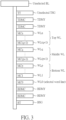
- FIG. 3 is a schematic diagram illustrating an unselected memory string and related connection lines of the non-volatile memory device 1 shown in FIG. 1 according to an embodiment of the present invention.
- FIG. 3 shows the unselected bit line BL, the top select gate line TSG, the top dummy word lines TDMY, the word lines WL0 to WLn, the bottom dummy word lines BDMY and the bottom select gate line BSG.
- the word lines WL0 is the selected word line
- the word lines WL1 to WLn are divided into a first group of word lines (Bottom WL), a second group of word lines (Middle WL) and a third group of word lines (Top WL).
- the first group of word lines includes the word lines WL1 to WLp.
- the first group of word lines is between the selected word line (word line WL0) and the second group of word lines (Middle WL).
- the second group of word lines includes the word lines WL(p+1) to WLq.
- the second group of word lines is between the first group of word lines (Bottom WL) and the third group of word lines (Top WL).
- the third group of word lines (Top WL) includes the word lines WL(q+1) to WLn.
- the third group of word lines (Top WL) is between the second group of word lines (Middle WL) and the top dummy word lines TDMY.
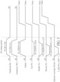
- FIG. 4 is a signal timing diagram of the memory string shown in FIG. 3 according to an embodiment of the present invention. Sequentially from the top of FIG. 4 , the signal waveforms in a pre-charge period are: a bit line pre-pulse signal VP_BL, a top select gate pre-pulse signal VP_TSG, a top dummy word line pre-pulse signal VP_TDMY, word line pre-pulse signals VP_TOPWL, VP_MIDDLEWL and VP_BOTTOMWL and a word line signal V_SELWL.
- the bit line pre-pulse signal VP_BL is applied to the unselected bit line BL of the unselected memory string of the memory array 10.
- the top select gate pre-pulse signal VP_TSG is applied to the top select gate line TSG.
- the top dummy word line pre-pulse signal VP_TDMY is applied to the top dummy word lines TDMY.
- the word line pre-pulse signals VP_TOPWL is applied to the third group of word lines (Top WL).
- the word line pre-pulse signals VP_MIDDLEWL is applied to the second group of word lines (Middle WL).
- the word line pre-pulse signals VP_BOTTOMWL is applied to the first group of word lines (Bottom WL).
- the bit line pre-pulse signal VP_BL applied to the unselected bit line BL may be a first power supply voltage Vdd.
- the top select gate pre-pulse signal VP_TSG applied to the top select gate line TSG may be a second power supply voltage Vcc.
- the top dummy word line pre-pulse signal VP_TDMY applied to the top dummy word lines TDMY may also be the first power supply voltage Vdd.
- the word line signal V_SELWL applied to the selected word line (WL0) can be a programming voltage.
- the voltage level (1.2 volts) of the word line pre-pulse signal VP_MIDDLEWL is greater than the voltage level (0.6 volts) of the word line pre-pulse signal VP_BOTTOMWL.
- the voltage level (1.8 volts) of the word line pre-pulse signal VP_ TOPWL is greater than the voltage level (1.2 volts) of the word line pre-pulse signal VP_MIDDLEWL.
- the voltage level (Vdd) of top dummy word line pre-pulse signal VP_TDMY is greater than the voltage levels of the word line pre-pulse signals VP_TOPWL, VP_MIDDLEWL and VP_BOTTOMWL.
- FIG. 5 is a signal timing diagram of the memory string shown in FIG. 3 according to an alternative embodiment of the present invention. Sequentially from the top of FIG. 5 , the signal waveforms in a pre-charge period are: a bit line pre-pulse signal VP_BL, a top select gate pre-pulse signal VP_TSG, a top dummy word line pre-pulse signal VP_TDMY, word line pre-pulse signals VP_TOPWL, VP_MIDDLEWL and VP_BOTTOMWL and a word line signal V_SELWL.
- the word line pre-pulse signals VP_TOPWL, VP_MIDDLEWL and VP_BOTTOMWL and the word line signal V_SELWL are negative pulse signals.
- the voltage level (-1.2 volts) of the word line pre-pulse signal VP_MIDDLEWL is greater than the voltage level (-1.8 volts) of the word line pre-pulse signal VP_BOTTOMWL.
- the voltage level (-0.6 volts) of the word line pre-pulse signal VP_ TOPWL is greater than the voltage level (-1.2 volts) of the word line pre-pulse signal VP_MIDDLEWL.
- the voltage level (Vdd) of top dummy word line pre-pulse signal VP_TDMY is greater than the voltage levels of the word line pre-pulse signals VP_TOPWL, VP_MIDDLEWL and VP_BOTTOMWL.
- the ending of the word line pre-pulse signal VP_MIDDLEWL applied to the second group of word lines occurs after the ending of the word line pre-pulse signal VP_BOTTOMWL applied to the first group of word lines (Bottom WL).
- the ending of the word line pre-pulse signal VP_TOPWL applied to the third group of word lines (Top WL) occurs after the ending of the word line pre-pulse signal VP _MIDDLEWL applied to the second group of word lines (Middle WL).
- the ending of the top dummy word line pre-pulse signal VP_TDMY applied to the top dummy word lines TDMY occurs after the endings of the word line pre-pulse signals VP_TOPWL, VP _MIDDLEWL and VP_BOTTOMWL.
- the end point of the word line pre-pulse signal VP_MIDDLEWL applied to the second group of word lines (Middle WL) is after the end point of the word line pre-pulse signal VP_ BOTTOMWL applied to the first group of word lines (Bottom WL) during the pre-charge period.
- the end point of the word line pre-pulse signal VP_TOPWL applied to the third group of word lines (Top WL) is after the end point of the word line pre-pulse signal VP_MIDDLEWL applied to the second group of word lines (Middle WL) during the pre-charge period.
- the end point of the top dummy word line pre-pulse signal VP_TDMY applied to the top dummy word lines TDMY is after the end points of the word line pre-pulse signals VP_TOPWL, VP_MIDDLEWL and VP_BOTTOMWL. Since the word line pre-pulse signals with different ending timing are applied to the word lines between the top select gate line and selected word line, the whole programming speed can be improved effectively.
- the falling edge of the word line pre-pulse signal VP_MIDDLEWL is after the falling edge of the word line pre-pulse signal VP_BOTTOMWL during the pre-charge period.
- the falling edge of the word line pre-pulse signal VP_TOPWL is after the falling edge of the word line pre-pulse signal VP_MIDDLEWL during the pre-charge period.
- the falling edge of the top dummy word line pre-pulse signal VP_TDMY applied to the top dummy word lines TDMY is after the falling edges of the word line pre-pulse signals VP_TOPWL, VP_MIDDLEWL and VP_BOTTOMWL.
- the word line pre-pulse signals VP_TOPWL, VP _MIDDLEWL and VP_BOTTOMWL are negative pulse signals
- the rising edge of the word line pre-pulse signal VP_MIDDLEWL is after the rising edge of the word line pre-pulse signal VP_ BOTTOMWL during the pre-charge period.
- the rising edge of the word line pre-pulse signal VP_TOPWL is after the rising edge of the word line pre-pulse signal VP _MIDDLEWL during the pre-charge period.
- the rising edge of the top dummy word line pre-pulse signal VP_TDMY is after the rising edges of the word line pre-pulse signals VP_TOPWL, VP_MIDDLEWL and VP_BOTTOMWL.
- the pulse durations (signal lengths) of the word line pre-pulse signals VP_TOPWL, VP_MIDDLEWL and VP_BOTTOMWL are incremental.
- the pulse duration of the word line pre-pulse signal VP _MIDDLEWL applied to the second group of word lines (Middle WL) is greater than the pulse duration of the word line pre-pulse signal VP_ BOTTOMWL applied to the first group of word lines (Bottom WL).
- the pulse duration of the word line pre-pulse signal VP_TOPWL applied to the third group of word lines (Top WL) is greater than the ending of the word line pre-pulse signal VP _MIDDLEWL applied to the second group of word lines (Middle WL).
- the pulse duration of the top dummy word line pre-pulse signal VP_TDMY applied to the top dummy word lines TDMY is greater than the pulse durations of the word line pre-pulse signals VP_TOPWL, VP_MIDDLEWL and VP_BOTTOMWL.
- the embodiments of the present invention provide word line pre-pulse signals with different to drive the word lines between the top select gate line and selected word line so as to enhance channel potential gradient, and thus enhancing the pre-charge effect of the unselected bit line and reducing programming disturb. Moreover, the embodiments of the present invention provide word line pre-pulse signals with different ending timing to the word lines between the top select gate line and selected word line, and thus improving the whole programming speed effectively.
Landscapes
- Engineering & Computer Science (AREA)
- Microelectronics & Electronic Packaging (AREA)
- Computer Hardware Design (AREA)
- Read Only Memory (AREA)
Priority Applications (1)
| Application Number | Priority Date | Filing Date | Title |
|---|---|---|---|
| EP25163660.1A EP4546343A3 (de) | 2019-10-22 | 2019-10-22 | Nichtflüchtige speichervorrichtung und steuerungsverfahren |
Applications Claiming Priority (4)
| Application Number | Priority Date | Filing Date | Title |
|---|---|---|---|
| EP23194703.7A EP4273866B1 (de) | 2019-10-22 | 2019-10-22 | Nichtflüchtige speichervorrichtung und steuerungsverfahren |
| PCT/CN2019/112409 WO2021077276A1 (en) | 2019-10-22 | 2019-10-22 | Non-volatile memory device and control method |
| EP25163660.1A EP4546343A3 (de) | 2019-10-22 | 2019-10-22 | Nichtflüchtige speichervorrichtung und steuerungsverfahren |
| EP19950116.4A EP3912164B1 (de) | 2019-10-22 | 2019-10-22 | Nichtflüchtige speichervorrichtung und steuerungsverfahren |
Related Parent Applications (3)
| Application Number | Title | Priority Date | Filing Date |
|---|---|---|---|
| EP23194703.7A Division EP4273866B1 (de) | 2019-10-22 | 2019-10-22 | Nichtflüchtige speichervorrichtung und steuerungsverfahren |
| EP23194703.7A Division-Into EP4273866B1 (de) | 2019-10-22 | 2019-10-22 | Nichtflüchtige speichervorrichtung und steuerungsverfahren |
| EP19950116.4A Division EP3912164B1 (de) | 2019-10-22 | 2019-10-22 | Nichtflüchtige speichervorrichtung und steuerungsverfahren |
Publications (2)
| Publication Number | Publication Date |
|---|---|
| EP4546343A2 true EP4546343A2 (de) | 2025-04-30 |
| EP4546343A3 EP4546343A3 (de) | 2025-09-17 |
Family
ID=69985840
Family Applications (3)
| Application Number | Title | Priority Date | Filing Date |
|---|---|---|---|
| EP25163660.1A Pending EP4546343A3 (de) | 2019-10-22 | 2019-10-22 | Nichtflüchtige speichervorrichtung und steuerungsverfahren |
| EP23194703.7A Active EP4273866B1 (de) | 2019-10-22 | 2019-10-22 | Nichtflüchtige speichervorrichtung und steuerungsverfahren |
| EP19950116.4A Active EP3912164B1 (de) | 2019-10-22 | 2019-10-22 | Nichtflüchtige speichervorrichtung und steuerungsverfahren |
Family Applications After (2)
| Application Number | Title | Priority Date | Filing Date |
|---|---|---|---|
| EP23194703.7A Active EP4273866B1 (de) | 2019-10-22 | 2019-10-22 | Nichtflüchtige speichervorrichtung und steuerungsverfahren |
| EP19950116.4A Active EP3912164B1 (de) | 2019-10-22 | 2019-10-22 | Nichtflüchtige speichervorrichtung und steuerungsverfahren |
Country Status (7)
| Country | Link |
|---|---|
| US (5) | US11081164B2 (de) |
| EP (3) | EP4546343A3 (de) |
| JP (3) | JP7282926B2 (de) |
| KR (2) | KR20250070140A (de) |
| CN (2) | CN113555053B (de) |
| TW (1) | TWI720748B (de) |
| WO (1) | WO2021077276A1 (de) |
Families Citing this family (8)
| Publication number | Priority date | Publication date | Assignee | Title |
|---|---|---|---|---|
| KR20250070140A (ko) * | 2019-10-22 | 2025-05-20 | 양쯔 메모리 테크놀로지스 씨오., 엘티디. | 비휘발성 메모리 장치 및 제어 방법 |
| US12412609B2 (en) | 2019-12-09 | 2025-09-09 | Yangtze Memory Technologies Co., Ltd. | Method of reducing program disturbance in memory device and memory device utilizing same |
| JP7132444B2 (ja) * | 2019-12-09 | 2022-09-06 | 長江存儲科技有限責任公司 | メモリデバイスにおけるプログラム撹乱低減方法およびそれを利用するメモリデバイス |
| CN111630600B (zh) * | 2020-04-15 | 2021-08-31 | 长江存储科技有限责任公司 | 3d nand闪存及其操作方法 |
| CN111758130B (zh) * | 2020-05-19 | 2021-04-16 | 长江存储科技有限责任公司 | 3d nand闪存及其操作方法 |
| CN113889170B (zh) * | 2021-01-06 | 2024-10-15 | 长江存储科技有限责任公司 | 用于半导体器件的编程方法及半导体器件 |
| WO2023070612A1 (en) | 2021-10-30 | 2023-05-04 | Yangtze Memory Technologies Co., Ltd. | Memory device and program operation thereof |
| CN120954466A (zh) * | 2024-05-14 | 2025-11-14 | 长江存储科技有限责任公司 | 存储器装置及其操作方法、存储器系统 |
Family Cites Families (44)
| Publication number | Priority date | Publication date | Assignee | Title |
|---|---|---|---|---|
| JP4156986B2 (ja) * | 2003-06-30 | 2008-09-24 | 株式会社東芝 | 不揮発性半導体記憶装置 |
| US7436709B2 (en) | 2006-05-05 | 2008-10-14 | Sandisk Corporation | NAND flash memory with boosting |
| US7511996B2 (en) * | 2006-11-30 | 2009-03-31 | Mosaid Technologies Incorporated | Flash memory program inhibit scheme |
| US7450430B2 (en) | 2006-12-29 | 2008-11-11 | Sandisk Corporation | Programming non-volatile memory with reduced program disturb by using different pre-charge enable voltages |
| US7463531B2 (en) * | 2006-12-29 | 2008-12-09 | Sandisk Corporation | Systems for programming non-volatile memory with reduced program disturb by using different pre-charge enable voltages |
| CN103137200A (zh) * | 2007-02-07 | 2013-06-05 | 莫塞德技术公司 | 源侧非对称预充电编程方案 |
| US7577026B2 (en) | 2007-05-07 | 2009-08-18 | Sandisk Corporation | Source and drain side early boosting using local self boosting for non-volatile storage |
| US7463522B2 (en) | 2007-05-07 | 2008-12-09 | Sandisk Corporation | Non-volatile storage with boosting using channel isolation switching |
| JP2009266946A (ja) | 2008-04-23 | 2009-11-12 | Toshiba Corp | 三次元積層不揮発性半導体メモリ |
| KR101635502B1 (ko) * | 2009-07-22 | 2016-07-01 | 삼성전자주식회사 | 반도체 메모리 장치 및 그것의 프로그램 방법 |
| KR20110032797A (ko) * | 2009-09-24 | 2011-03-30 | 주식회사 하이닉스반도체 | 불휘발성 메모리 소자의 프로그램 방법 |
| US8638609B2 (en) | 2010-05-19 | 2014-01-28 | Spansion Llc | Partial local self boosting for NAND |
| KR101868393B1 (ko) * | 2012-03-14 | 2018-06-21 | 삼성전자주식회사 | 불휘발성 메모리 장치 및 불휘발성 메모리 장치의 프로그램 방법 |
| KR102081749B1 (ko) * | 2013-02-20 | 2020-02-26 | 삼성전자주식회사 | 메모리 시스템 및 그것의 프로그램 방법 |
| JP2015026406A (ja) * | 2013-07-24 | 2015-02-05 | 株式会社東芝 | 不揮発性半導体記憶装置 |
| KR102116668B1 (ko) * | 2014-02-04 | 2020-05-29 | 삼성전자주식회사 | 불 휘발성 메모리 장치 및 불 휘발성 메모리 장치의 동작 방법 |
| JP2015176620A (ja) * | 2014-03-14 | 2015-10-05 | 株式会社東芝 | 半導体記憶装置 |
| KR102248267B1 (ko) * | 2014-04-30 | 2021-05-07 | 삼성전자주식회사 | 비휘발성 메모리 장치, 그것을 포함하는 저장 장치 및 그것의 동작 및 읽기 방법들 |
| US9460805B1 (en) * | 2015-10-19 | 2016-10-04 | Sandisk Technologies Llc | Word line dependent channel pre-charge for memory |
| US9589978B1 (en) | 2016-02-25 | 2017-03-07 | Micron Technology, Inc. | Memory devices with stairs in a staircase coupled to tiers of memory cells and to pass transistors directly under the staircase |
| KR102620562B1 (ko) * | 2016-08-04 | 2024-01-03 | 삼성전자주식회사 | 비휘발성 메모리 장치 |
| US11017838B2 (en) * | 2016-08-04 | 2021-05-25 | Samsung Electronics Co., Ltd. | Nonvolatile memory devices |
| KR102633029B1 (ko) * | 2016-08-22 | 2024-02-06 | 삼성전자주식회사 | 불휘발성 메모리 장치, 불휘발성 메모리 장치를 포함하는 스토리지 장치 및 불휘발성 메모리 장치의 읽기 방법 |
| KR102533197B1 (ko) * | 2016-09-22 | 2023-05-17 | 에스케이하이닉스 주식회사 | 반도체 메모리 장치 및 그 동작 방법 |
| KR102579879B1 (ko) * | 2016-11-14 | 2023-09-18 | 삼성전자주식회사 | 비휘발성 메모리 장치 및 그 독출 방법 |
| JP2018125052A (ja) * | 2017-01-31 | 2018-08-09 | 東芝メモリ株式会社 | 半導体記憶装置 |
| KR102683413B1 (ko) * | 2017-02-02 | 2024-07-10 | 삼성전자주식회사 | 비휘발성 메모리 장치, 비휘발성 메모리 장치의 소프트 이레이즈 방법 및 프로그램 방법 |
| US10297323B2 (en) | 2017-10-06 | 2019-05-21 | Sandisk Technologies Llc | Reducing disturbs with delayed ramp up of dummy word line after pre-charge during programming |
| US10283202B1 (en) * | 2017-11-16 | 2019-05-07 | Sandisk Technologies Llc | Reducing disturbs with delayed ramp up of selected word line voltage after pre-charge during programming |
| US10276250B1 (en) | 2017-11-20 | 2019-04-30 | Macronix International Co., Ltd. | Programming NAND flash with improved robustness against dummy WL disturbance |
| US10720197B2 (en) * | 2017-11-21 | 2020-07-21 | Samsung Electronics Co., Ltd. | Memory device for supporting command bus training mode and method of operating the same |
| AU2018371302B2 (en) * | 2017-11-23 | 2020-07-16 | Fatty Industries Pty Ltd | Exercise bay and exercise apparatus for use with same |
| JP2019109952A (ja) * | 2017-12-19 | 2019-07-04 | 東芝メモリ株式会社 | 半導体記憶装置 |
| US10643718B2 (en) * | 2018-06-07 | 2020-05-05 | Sandisk Technologies Llc | Non-volatile memory with countermeasure for program disturb including purge during precharge |
| JP2020004470A (ja) | 2018-06-29 | 2020-01-09 | キオクシア株式会社 | 半導体記憶装置 |
| US10726920B2 (en) | 2018-11-26 | 2020-07-28 | Sandisk Technologies Llc | Pre-charge voltage for inhibiting unselected NAND memory cell programming |
| US10770157B1 (en) * | 2019-05-21 | 2020-09-08 | Sandisk Technologies Llc | Method of reducing injection type of program disturb during program pre-charge in memory device |
| CN110289034A (zh) * | 2019-06-28 | 2019-09-27 | 长江存储科技有限责任公司 | 非易失性存储器及其操作方法 |
| CN112652345B (zh) * | 2019-10-12 | 2022-10-28 | 长江存储科技有限责任公司 | 对存储器件进行编程的方法及相关存储器件 |
| KR20250070140A (ko) * | 2019-10-22 | 2025-05-20 | 양쯔 메모리 테크놀로지스 씨오., 엘티디. | 비휘발성 메모리 장치 및 제어 방법 |
| WO2021077314A1 (en) * | 2019-10-23 | 2021-04-29 | Yangtze Memory Technologies Co., Ltd. | Method of programming memory device and related memory device |
| JP7181419B2 (ja) * | 2019-10-31 | 2022-11-30 | 長江存儲科技有限責任公司 | 不揮発性メモリデバイスおよび制御方法 |
| KR102780354B1 (ko) * | 2019-12-26 | 2025-03-12 | 삼성전자주식회사 | 메모리 장치 및 그 동작 방법 |
| CN111758130B (zh) * | 2020-05-19 | 2021-04-16 | 长江存储科技有限责任公司 | 3d nand闪存及其操作方法 |
-
2019
- 2019-10-22 KR KR1020257015897A patent/KR20250070140A/ko active Pending
- 2019-10-22 CN CN202110850553.6A patent/CN113555053B/zh active Active
- 2019-10-22 JP JP2021576682A patent/JP7282926B2/ja active Active
- 2019-10-22 EP EP25163660.1A patent/EP4546343A3/de active Pending
- 2019-10-22 CN CN201980002808.4A patent/CN110959177B/zh active Active
- 2019-10-22 KR KR1020217042152A patent/KR102811362B1/ko active Active
- 2019-10-22 EP EP23194703.7A patent/EP4273866B1/de active Active
- 2019-10-22 EP EP19950116.4A patent/EP3912164B1/de active Active
- 2019-10-22 WO PCT/CN2019/112409 patent/WO2021077276A1/en not_active Ceased
- 2019-12-11 US US16/709,944 patent/US11081164B2/en active Active
- 2019-12-18 TW TW108146384A patent/TWI720748B/zh active
-
2021
- 2021-06-21 US US17/353,727 patent/US11501822B2/en active Active
-
2022
- 2022-10-13 US US17/965,527 patent/US11862230B2/en active Active
-
2023
- 2023-05-16 JP JP2023080950A patent/JP7541156B2/ja active Active
- 2023-11-06 US US18/387,204 patent/US12512145B2/en active Active
-
2024
- 2024-08-14 JP JP2024135476A patent/JP7728936B2/ja active Active
- 2024-11-29 US US18/964,165 patent/US20250095715A1/en active Pending
Also Published As
Similar Documents
| Publication | Publication Date | Title |
|---|---|---|
| US12512145B2 (en) | Non-volatile memory device and control method | |
| CN111033626B (zh) | 非易失性存储器件和控制方法 | |
| US10699789B2 (en) | Nonvolatile memory device and memory system including nonvolatile memory device that controls the erase speeds of cell strings | |
| US8867273B2 (en) | Non-volatile semiconductor memory device and method of writing data therein | |
| CN111712877B (zh) | 非易失性存储器件及其控制方法 | |
| CN121281590A (zh) | 存储器装置和存储器装置的信息数据读取方法 | |
| CN114758691A (zh) | 沟道预充电方法、编程方法、装置及系统 |
Legal Events
| Date | Code | Title | Description |
|---|---|---|---|
| PUAI | Public reference made under article 153(3) epc to a published international application that has entered the european phase |
Free format text: ORIGINAL CODE: 0009012 |
|
| STAA | Information on the status of an ep patent application or granted ep patent |
Free format text: STATUS: REQUEST FOR EXAMINATION WAS MADE |
|
| 17P | Request for examination filed |
Effective date: 20250313 |
|
| AC | Divisional application: reference to earlier application |
Ref document number: 3912164 Country of ref document: EP Kind code of ref document: P Ref document number: 4273866 Country of ref document: EP Kind code of ref document: P |
|
| AK | Designated contracting states |
Kind code of ref document: A2 Designated state(s): AL AT BE BG CH CY CZ DE DK EE ES FI FR GB GR HR HU IE IS IT LI LT LU LV MC MK MT NL NO PL PT RO RS SE SI SK SM TR |
|
| PUAL | Search report despatched |
Free format text: ORIGINAL CODE: 0009013 |
|
| AK | Designated contracting states |
Kind code of ref document: A3 Designated state(s): AL AT BE BG CH CY CZ DE DK EE ES FI FR GB GR HR HU IE IS IT LI LT LU LV MC MK MT NL NO PL PT RO RS SE SI SK SM TR |
|
| RIC1 | Information provided on ipc code assigned before grant |
Ipc: G11C 16/34 20060101AFI20250814BHEP |
|
| GRAP | Despatch of communication of intention to grant a patent |
Free format text: ORIGINAL CODE: EPIDOSNIGR1 |
|
| STAA | Information on the status of an ep patent application or granted ep patent |
Free format text: STATUS: GRANT OF PATENT IS INTENDED |
|
| INTG | Intention to grant announced |
Effective date: 20251218 |
|
| GRAS | Grant fee paid |
Free format text: ORIGINAL CODE: EPIDOSNIGR3 |
|
| GRAA | (expected) grant |
Free format text: ORIGINAL CODE: 0009210 |
|
| STAA | Information on the status of an ep patent application or granted ep patent |
Free format text: STATUS: THE PATENT HAS BEEN GRANTED |