EP4394517A1 - Image forming apparatus - Google Patents
Image forming apparatus Download PDFInfo
- Publication number
- EP4394517A1 EP4394517A1 EP23219137.9A EP23219137A EP4394517A1 EP 4394517 A1 EP4394517 A1 EP 4394517A1 EP 23219137 A EP23219137 A EP 23219137A EP 4394517 A1 EP4394517 A1 EP 4394517A1
- Authority
- EP
- European Patent Office
- Prior art keywords
- charging
- bearing member
- image
- developer
- photosensitive drum
- Prior art date
- Legal status (The legal status is an assumption and is not a legal conclusion. Google has not performed a legal analysis and makes no representation as to the accuracy of the status listed.)
- Pending
Links
Images


Classifications
-
- G—PHYSICS
- G03—PHOTOGRAPHY; CINEMATOGRAPHY; ANALOGOUS TECHNIQUES USING WAVES OTHER THAN OPTICAL WAVES; ELECTROGRAPHY; HOLOGRAPHY
- G03G—ELECTROGRAPHY; ELECTROPHOTOGRAPHY; MAGNETOGRAPHY
- G03G15/00—Apparatus for electrographic processes using a charge pattern
- G03G15/02—Apparatus for electrographic processes using a charge pattern for laying down a uniform charge, e.g. for sensitising; Corona discharge devices
- G03G15/0208—Apparatus for electrographic processes using a charge pattern for laying down a uniform charge, e.g. for sensitising; Corona discharge devices by contact, friction or induction, e.g. liquid charging apparatus
- G03G15/0216—Apparatus for electrographic processes using a charge pattern for laying down a uniform charge, e.g. for sensitising; Corona discharge devices by contact, friction or induction, e.g. liquid charging apparatus by bringing a charging member into contact with the member to be charged, e.g. roller, brush chargers
- G03G15/0225—Apparatus for electrographic processes using a charge pattern for laying down a uniform charge, e.g. for sensitising; Corona discharge devices by contact, friction or induction, e.g. liquid charging apparatus by bringing a charging member into contact with the member to be charged, e.g. roller, brush chargers provided with means for cleaning the charging member
-
- G—PHYSICS
- G03—PHOTOGRAPHY; CINEMATOGRAPHY; ANALOGOUS TECHNIQUES USING WAVES OTHER THAN OPTICAL WAVES; ELECTROGRAPHY; HOLOGRAPHY
- G03G—ELECTROGRAPHY; ELECTROPHOTOGRAPHY; MAGNETOGRAPHY
- G03G15/00—Apparatus for electrographic processes using a charge pattern
- G03G15/02—Apparatus for electrographic processes using a charge pattern for laying down a uniform charge, e.g. for sensitising; Corona discharge devices
- G03G15/0208—Apparatus for electrographic processes using a charge pattern for laying down a uniform charge, e.g. for sensitising; Corona discharge devices by contact, friction or induction, e.g. liquid charging apparatus
- G03G15/0216—Apparatus for electrographic processes using a charge pattern for laying down a uniform charge, e.g. for sensitising; Corona discharge devices by contact, friction or induction, e.g. liquid charging apparatus by bringing a charging member into contact with the member to be charged, e.g. roller, brush chargers
-
- G—PHYSICS
- G03—PHOTOGRAPHY; CINEMATOGRAPHY; ANALOGOUS TECHNIQUES USING WAVES OTHER THAN OPTICAL WAVES; ELECTROGRAPHY; HOLOGRAPHY
- G03G—ELECTROGRAPHY; ELECTROPHOTOGRAPHY; MAGNETOGRAPHY
- G03G15/00—Apparatus for electrographic processes using a charge pattern
- G03G15/02—Apparatus for electrographic processes using a charge pattern for laying down a uniform charge, e.g. for sensitising; Corona discharge devices
- G03G15/0266—Arrangements for controlling the amount of charge
-
- G—PHYSICS
- G03—PHOTOGRAPHY; CINEMATOGRAPHY; ANALOGOUS TECHNIQUES USING WAVES OTHER THAN OPTICAL WAVES; ELECTROGRAPHY; HOLOGRAPHY
- G03G—ELECTROGRAPHY; ELECTROPHOTOGRAPHY; MAGNETOGRAPHY
- G03G15/00—Apparatus for electrographic processes using a charge pattern
- G03G15/06—Apparatus for electrographic processes using a charge pattern for developing
- G03G15/065—Arrangements for controlling the potential of the developing electrode
-
- G—PHYSICS
- G03—PHOTOGRAPHY; CINEMATOGRAPHY; ANALOGOUS TECHNIQUES USING WAVES OTHER THAN OPTICAL WAVES; ELECTROGRAPHY; HOLOGRAPHY
- G03G—ELECTROGRAPHY; ELECTROPHOTOGRAPHY; MAGNETOGRAPHY
- G03G15/00—Apparatus for electrographic processes using a charge pattern
- G03G15/06—Apparatus for electrographic processes using a charge pattern for developing
- G03G15/08—Apparatus for electrographic processes using a charge pattern for developing using a solid developer, e.g. powder developer
- G03G15/0822—Arrangements for preparing, mixing, supplying or dispensing developer
- G03G15/0844—Arrangements for purging used developer from the developing unit
-
- G—PHYSICS
- G03—PHOTOGRAPHY; CINEMATOGRAPHY; ANALOGOUS TECHNIQUES USING WAVES OTHER THAN OPTICAL WAVES; ELECTROGRAPHY; HOLOGRAPHY
- G03G—ELECTROGRAPHY; ELECTROPHOTOGRAPHY; MAGNETOGRAPHY
- G03G15/00—Apparatus for electrographic processes using a charge pattern
- G03G15/14—Apparatus for electrographic processes using a charge pattern for transferring a pattern to a second base
- G03G15/16—Apparatus for electrographic processes using a charge pattern for transferring a pattern to a second base of a toner pattern, e.g. a powder pattern, e.g. magnetic transfer
- G03G15/1665—Apparatus for electrographic processes using a charge pattern for transferring a pattern to a second base of a toner pattern, e.g. a powder pattern, e.g. magnetic transfer by introducing the second base in the nip formed by the recording member and at least one transfer member, e.g. in combination with bias or heat
- G03G15/167—Apparatus for electrographic processes using a charge pattern for transferring a pattern to a second base of a toner pattern, e.g. a powder pattern, e.g. magnetic transfer by introducing the second base in the nip formed by the recording member and at least one transfer member, e.g. in combination with bias or heat at least one of the recording member or the transfer member being rotatable during the transfer
- G03G15/1675—Apparatus for electrographic processes using a charge pattern for transferring a pattern to a second base of a toner pattern, e.g. a powder pattern, e.g. magnetic transfer by introducing the second base in the nip formed by the recording member and at least one transfer member, e.g. in combination with bias or heat at least one of the recording member or the transfer member being rotatable during the transfer with means for controlling the bias applied in the transfer nip
-
- G—PHYSICS
- G03—PHOTOGRAPHY; CINEMATOGRAPHY; ANALOGOUS TECHNIQUES USING WAVES OTHER THAN OPTICAL WAVES; ELECTROGRAPHY; HOLOGRAPHY
- G03G—ELECTROGRAPHY; ELECTROPHOTOGRAPHY; MAGNETOGRAPHY
- G03G15/00—Apparatus for electrographic processes using a charge pattern
- G03G15/50—Machine control of apparatus for electrographic processes using a charge pattern, e.g. regulating differents parts of the machine, multimode copiers, microprocessor control
- G03G15/5008—Driving control for rotary photosensitive medium, e.g. speed control, stop position control
-
- G—PHYSICS
- G03—PHOTOGRAPHY; CINEMATOGRAPHY; ANALOGOUS TECHNIQUES USING WAVES OTHER THAN OPTICAL WAVES; ELECTROGRAPHY; HOLOGRAPHY
- G03G—ELECTROGRAPHY; ELECTROPHOTOGRAPHY; MAGNETOGRAPHY
- G03G21/00—Arrangements not provided for by groups G03G13/00 - G03G19/00, e.g. cleaning, elimination of residual charge
- G03G21/0005—Arrangements not provided for by groups G03G13/00 - G03G19/00, e.g. cleaning, elimination of residual charge for removing solid developer or debris from the electrographic recording medium
- G03G21/0011—Arrangements not provided for by groups G03G13/00 - G03G19/00, e.g. cleaning, elimination of residual charge for removing solid developer or debris from the electrographic recording medium using a blade; Details of cleaning blades, e.g. blade shape, layer forming
-
- G—PHYSICS
- G03—PHOTOGRAPHY; CINEMATOGRAPHY; ANALOGOUS TECHNIQUES USING WAVES OTHER THAN OPTICAL WAVES; ELECTROGRAPHY; HOLOGRAPHY
- G03G—ELECTROGRAPHY; ELECTROPHOTOGRAPHY; MAGNETOGRAPHY
- G03G9/00—Developers
- G03G9/08—Developers with toner particles
- G03G9/097—Plasticisers; Charge controlling agents
-
- G—PHYSICS
- G03—PHOTOGRAPHY; CINEMATOGRAPHY; ANALOGOUS TECHNIQUES USING WAVES OTHER THAN OPTICAL WAVES; ELECTROGRAPHY; HOLOGRAPHY
- G03G—ELECTROGRAPHY; ELECTROPHOTOGRAPHY; MAGNETOGRAPHY
- G03G21/00—Arrangements not provided for by groups G03G13/00 - G03G19/00, e.g. cleaning, elimination of residual charge
- G03G21/0005—Arrangements not provided for by groups G03G13/00 - G03G19/00, e.g. cleaning, elimination of residual charge for removing solid developer or debris from the electrographic recording medium
- G03G21/0064—Arrangements not provided for by groups G03G13/00 - G03G19/00, e.g. cleaning, elimination of residual charge for removing solid developer or debris from the electrographic recording medium using the developing unit, e.g. cleanerless or multi-cycle apparatus
Definitions
- a technique for stabilizing the charging performance by using inorganic particles showing charge polarity opposite to that of a toner as an external additive has been reported as a means for increasing the charging performance of the toner.
- a technique for stabilizing the charging performance by using a titanic acid compound represented by strontium titanate as an external additive is publicly known as disclosed in Japanese Patent Application Publication No. 2001-290302 .
- the occurrence of fogging can be suppressed to some extent.
- the present invention provides a technique that can maintain good image quality during long-term use of an image forming apparatus.
- the present invention in its one aspect provides an image forming apparatus as specified in claims 1 to 16.
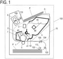
- FIG. 1 is a cross-sectional view of a schematic configuration of an image forming apparatus according to an example of the present invention, the configuration being shown in a simplified manner.
- the image forming apparatus to which the present invention is assumed to be applied is typically an image forming apparatus using an electrophotographic recording method, such as a laser printer, a copying machine, or a facsimile.
- a so-called monochrome image forming apparatus that is, an image forming apparatus equipped with a single image forming unit
- the image forming apparatus to which the present invention is applicable is not limited to this.
- the present invention can be suitably applied to a so-called full-color image forming apparatus, that is, an image forming apparatus equipped with a plurality of image forming units.
- the first difference in device configuration between a monochrome image forming apparatus and a color image forming apparatus is that the colors and number of colors of images formed are different.
- an image of a single color typically black
- images of freely determined colors can be formed by superimposing a plurality of developer images of different colors on each other.
- an intermediate transfer type color image forming apparatus a developer image is first transferred from a photosensitive member as an image bearing member to an intermediate transfer member (also referred to as a second image bearing member) as a first transferred member. The image is then transferred from the intermediate transfer member to a recording material serving as a second transferred member.
- a monochrome image forming apparatus or a direct transfer type color image forming apparatus a developer image is directly transferred from a photosensitive member to a recording material.
- An image forming apparatus 100 includes a process cartridge 10.
- the process cartridge 10 includes a photosensitive drum 1 as an image bearing member.
- a charging roller 2 as a charging member for charging the surface of the photosensitive drum 1
- a developing roller 41 as a developer bearing member for developing an electrostatic image formed on the surface of the photosensitive drum 1 with developer 44 are provided around the photosensitive drum 1 of the process cartridge 10.
- the process cartridge 10 further includes a developing blade 43 as a developer regulating member that regulates and charges the toner on the developing roller 41, and a supply roller (toner supplying member) 42 that supplies toner to and strips toner from the developing roller 41.
- the formed electrostatic latent image is developed as a toner image (developer image) by the toner holding a normal charge that was formed on the developing roller 41.
- the image forming apparatus 100 is equipped with power supplies (see FIG. 13 ) for applying predetermined voltages to each of the charging roller 2, developing roller 41, developing blade 43, supply roller 42, and transfer roller 5.
- the photosensitive drum 1 is a photosensitive member formed in a cylindrical shape.
- the photosensitive drum 1 of the present embodiment has a photosensitive layer formed of a negatively chargeable organic photosensitive member on a drum-shaped base made of aluminum.
- the photosensitive drum 1 has a diameter of 24 mm and is rotationally driven by a motor in a predetermined direction (clockwise in the figure) at a predetermined process speed.
- the photosensitive drum 1 of the present embodiment is rotationally driven at a process speed of 260 mm/sec.
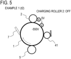
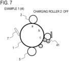
- the charging roller 2 has a diameter of 8.5 mm and contacts the photosensitive drum 1 with a predetermined pressing force to form a charging portion. Further, the charging roller 2 uniformly charges the surface of the photosensitive drum 1 to a predetermined potential by applying a desired charging voltage from a charging high-voltage power supply. In the present embodiment, the photosensitive drum 1 is negatively charged by the charging roller 2.
- the developing device portion of the process cartridge 10 includes a developing roller 41 as a developer bearing member that bears the developer, a developer container 4 serving as a frame constituting a developer storage portion, and a supply roller 42 that can supply the developer 44 to the developing roller 41.
- the developing roller 41 and the supply roller 42 are rotatably supported by the developer container 4. Further, the developing roller 41 has a diameter of 10 mm and is arranged at the opening portion of the developer container 4 so as to face the photosensitive drum 1.
- the supply roller 42 abuts rotatably against the developing roller 41, and the toner contained as the developer 44 in the developer container 4 is applied to the surface of the developing roller 41 by the supply roller 42.
- the supply roller 42 is not necessarily required if the configuration is such that the toner can be sufficiently supplied to the developing roller 41.
- the process cartridge 10 of the present embodiment uses a contact development method as a development method. That is, the toner layer supported on the developing roller 41 comes into contact with the photosensitive drum 1 in a development portion (development region) where the photosensitive drum 1 and the developing roller 41 face each other.
- a developing voltage is applied to the developing roller 41 by a development high-voltage power supply. Under the developing voltage, the toner borne on the developing roller 41 is transferred from the developing roller 41 to the drum surface according to the potential distribution on the surface of the photosensitive drum 1, whereby the electrostatic latent image is developed into a toner image.
- a reversal development method is used. That is, after being charged in the charging step, toner adheres to the surface region of the photosensitive drum 1 where the charge quantity has been attenuated by the exposure in the exposure step, thereby forming a toner image.
- the one-component developer may contain additives as external additives for the purpose of modifying the surface properties in order to adjust the flowability and charging capability of the toner.
- additives as external additives for the purpose of modifying the surface properties in order to adjust the flowability and charging capability of the toner.
- an inorganic salt on the toner surface. Examples of the inorganic salts to be formed on the toner surface used in the present embodiment include silica, alumina, titanium oxide, aluminum oxide, barium titanate, magnesium titanate, calcium titanate, and strontium titanate.
- zinc oxide, tin oxide, silica sand, clay, mica, wollastonite, diatomaceous earth, chromium oxide, cerium oxide, red iron oxide, antimony trioxide, and magnesium oxide can also be used.
- zirconium oxide, barium sulfate, barium carbonate, calcium carbonate, silicon carbide, silicon nitride, and the like can also be used.
- these external additives can be sometimes referred to as positive external additives, that is, positive-charging external additives of charge polarity opposite to the toner having negative charge polarity as normal polarity.
- a two-component developer composed of a non-magnetic toner and a magnetic carrier may be used as the developer.
- the developer bearing member When using a magnetic developer, for example, a cylindrical developing sleeve with a magnet disposed inside is used as the developer bearing member. That is, here, the developer can be in the form consisting only of toner particles, the form consisting of toner particles and an additive or a carrier, and the like. In the following explanation, developers inclusive of these various forms may be referred to as toner 44.
- the developing roller 41 is disposed to face the photosensitive drum 1 and be in contact therewith in the development portion and is driven to rotate at a predetermined speed.
- the developing roller 41 in the present example is in contact with the photosensitive drum 1 at all times while the process cartridge 10 is mounted on the main body of the image forming apparatus 100, even when no image is formed. That is, the image forming apparatus 100 is not provided with an abutment/separation mechanism for separating the developing roller 41 from the photosensitive drum 1.
- a fixing portion 6 is of a heat fixing type that fixes the image by heating and melting the toner on the recording material P.
- the fixing portion 6 includes a fixing film, a fixing heater such as a ceramic heater that heats the fixing film, a thermistor that measures the temperature of the fixing heater, and a pressure roller that presses against the fixing film.
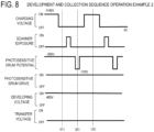
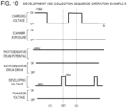
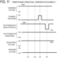
- a controller 201 is capable of communicating with a host computer 200 and an engine control portion 202. Where print data are input from the host computer 200, the controller 201 develops the print data and converts it into image data for image formation. Then, an exposure video signal is generated for exposure based on the image data. When the generation of the video signal is completed, the controller 201 instructs a video interface portion 210 of an engine control portion 202 to start forming an image using a command. After that, when an instruction to start image formation is received from the video interface portion 210, CPU 220 starts various actuators such as the main motor 250 and starts preparing for image formation. When the preparation for image formation is completed, the engine control portion 202 starts outputting a BD signal, which is the reference timing for outputting the video signal, to the controller 201, and sequentially executes the above-described image forming operations.
- BD signal which is the reference timing for outputting the video signal
- the voltage control portion 230 is configured (transfer voltage applying portion) to be capable of applying a voltage of positive polarity to the transfer roller 5 from a high-voltage power supply TPp for applying a transfer voltage (positive voltage applying portion) and applying a voltage of negative polarity to the transfer roller 5 from a power supply TPn for applying a non-transfer voltage (negative voltage applying portion).
- the polarities of these voltages are based on the premise that the normal charging polarity of the toner is negative. Therefore, it goes without saying that when the normal charging polarity of the toner is positive, the polarities of the voltages described above are reversed.
- the relative arrangement of each member around the circumferential surface of the rotating photosensitive drum 1 will be explained hereinbelow.
- the position around the circumferential surface of the rotating photosensitive drum 1 where the photosensitive drum 1 and the charging roller 2 abut against each other is defined as a charging position (charging portion (a)).
- An exposure position (scan exposure portion (b)) which is irradiated by laser light emitted from the scanner unit 3 is formed downstream of this charging position in the direction of the photosensitive drum 1 around the circumferential surface of the photosensitive drum 1.
- the photosensitive drum 1 is charged in advance by the charging roller 2, and an electrostatic latent image is formed on the photosensitive drum 1 as a result of irradiation with the laser light. Thereafter, this electrostatic latent image is developed by the developing roller 41, and a toner image is formed on the photosensitive drum 1.
- a transfer voltage is applied from the transfer high-voltage power supply TPp to the transfer roller 5 as a transfer member, and the toner image borne on the photosensitive drum 1 is transferred onto the recording material P conveyed by the resist roller pair.
- the recording material P onto which the toner image has been transferred is conveyed to the fixing portion 6, and the toner image is heated and pressed when passing through the nip between the fixing film of the fixing portion 6 and the pressure roller. As a result, the toner particles are melted and then fixed, thereby fixing the toner image on the recording material P.
- the exposure amount and exposure area are determined according to the image signal.
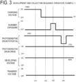
- the image formation portion is exposed to light by the scanner unit 3, and adjusted to a post-exposure potential Vl (light area potential: -170 V), which is the image area potential.
- the exposure amount E0 to form this Vl was set to 0.24 ⁇ J/cm 2 .
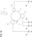
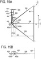
- FIGS. 15A and 15B are configuration diagrams of the scanner unit 3 of the present example, with FIG. 15A showing a cross-sectional view in the main scanning direction and FIG. 15B showing a cross-sectional view in the sub-scanning direction.
- the main scanning direction is a direction parallel to the surface of the photosensitive drum 1 and perpendicular to the movement direction of the surface of the photosensitive drum 1.
- the sub-scanning direction is the movement direction of the surface of the photosensitive drum 1.
- a laser beam 208 emitted from a light source 401 is shaped into an elliptical form by an aperture 402 and falls on a coupling lens 403.
- the laser beam 208 that has passed through the coupling lens 403 is converted into a substantially parallel light beam and falls on an anamorphic lens 404.
- the substantially parallel light beam is inclusive of a weakly convergent light beam and a weakly diverging light beam.
- the anamorphic lens 404 has a positive refractive power within the main scanning cross-section, and converts the incident light beam into a convergent light beam within the main scanning cross-section. Further, the anamorphic lens 404 focuses the light flux near a reflective surface 405a of a deflector (polygon mirror) 405 within the sub-scanning cross-section, and forms a long linear image in the main scanning direction.
- the light flux that has passed through the anamorphic lens 404 is reflected by the reflective surface 405a of the deflector 405.
- the laser beam 208 reflected by the reflective surface 405a passes through an imaging lens 406, forms an image on the surface of the photosensitive drum 1 and forms a predetermined spot-shaped image (hereinafter referred to as a spot).
- a spot As a result of rotating the deflector 405 at a constant angular velocity in the direction of arrow Ao by a drive unit (not shown), the spot moves in the main scanning direction on a surface 407 to be scanned of the photosensitive drum 1, and an electrostatic latent image is formed on the surface 407.
- An image forming apparatus is characterized by that a region of the surface of an image bearing member in which a second potential difference that generates an electrostatic force such that developer which is charged to an opposite polarity to the normal charging polarity of the developer moves from the image bearing member to a developer bearing member was generated in a second operation that moves the developer from the surface of the image bearing member to the developer bearing member includes a region where a first potential difference that generates an electrostatic force such that the developer which is charged to an opposite polarity to the normal charging polarity of the developer moves from the charging member to the image bearing member was generated in a first operation that moves the developer from the surface of the charging member to the surface of the image bearing member.
Landscapes
- Physics & Mathematics (AREA)
- General Physics & Mathematics (AREA)
- Engineering & Computer Science (AREA)
- Plasma & Fusion (AREA)
- Microelectronics & Electronic Packaging (AREA)
- Electrostatic Charge, Transfer And Separation In Electrography (AREA)
- Dry Development In Electrophotography (AREA)
- Cleaning In Electrography (AREA)
- Control Or Security For Electrophotography (AREA)
Applications Claiming Priority (1)
| Application Number | Priority Date | Filing Date | Title |
|---|---|---|---|
| JP2022212533A JP2024095328A (ja) | 2022-12-28 | 2022-12-28 | 画像形成装置 |
Publications (1)
| Publication Number | Publication Date |
|---|---|
| EP4394517A1 true EP4394517A1 (en) | 2024-07-03 |
Family
ID=89308528
Family Applications (1)
| Application Number | Title | Priority Date | Filing Date |
|---|---|---|---|
| EP23219137.9A Pending EP4394517A1 (en) | 2022-12-28 | 2023-12-21 | Image forming apparatus |
Country Status (3)
| Country | Link |
|---|---|
| US (1) | US12313982B2 (enExample) |
| EP (1) | EP4394517A1 (enExample) |
| JP (1) | JP2024095328A (enExample) |
Families Citing this family (1)
| Publication number | Priority date | Publication date | Assignee | Title |
|---|---|---|---|---|
| JP2025018760A (ja) * | 2023-07-27 | 2025-02-06 | キヤノン株式会社 | 画像形成装置 |
Citations (4)
| Publication number | Priority date | Publication date | Assignee | Title |
|---|---|---|---|---|
| JP2001290302A (ja) | 2000-04-06 | 2001-10-19 | Konica Corp | 静電荷像現像用トナーと画像形成方法 |
| US20160097986A1 (en) * | 2014-10-01 | 2016-04-07 | Canon Kabushiki Kaisha | Image forming apparatus |
| JP2022092546A (ja) | 2020-12-10 | 2022-06-22 | キヤノン株式会社 | トナー |
| US20220269206A1 (en) * | 2021-02-24 | 2022-08-25 | Canon Kabushiki Kaisha | Image forming apparatus |
Family Cites Families (8)
| Publication number | Priority date | Publication date | Assignee | Title |
|---|---|---|---|---|
| JP2007093981A (ja) | 2005-09-28 | 2007-04-12 | Kyocera Mita Corp | 画像形成装置 |
| JP5023643B2 (ja) | 2006-10-05 | 2012-09-12 | コニカミノルタビジネステクノロジーズ株式会社 | 画像形成装置 |
| JP6265695B2 (ja) | 2013-11-13 | 2018-01-24 | キヤノン株式会社 | 画像形成装置 |
| JP6271958B2 (ja) | 2013-11-13 | 2018-01-31 | キヤノン株式会社 | 画像形成装置 |
| JP6162040B2 (ja) | 2013-12-26 | 2017-07-12 | 株式会社沖データ | 画像形成装置 |
| JP7027119B2 (ja) * | 2017-10-24 | 2022-03-01 | キヤノン株式会社 | 画像形成装置 |
| JP2020079902A (ja) * | 2018-11-14 | 2020-05-28 | キヤノン株式会社 | 画像形成装置及びプロセスカートリッジ |
| JP2024046724A (ja) | 2022-09-24 | 2024-04-04 | キヤノン株式会社 | 画像形成装置 |
-
2022
- 2022-12-28 JP JP2022212533A patent/JP2024095328A/ja active Pending
-
2023
- 2023-12-21 EP EP23219137.9A patent/EP4394517A1/en active Pending
- 2023-12-22 US US18/394,127 patent/US12313982B2/en active Active
Patent Citations (4)
| Publication number | Priority date | Publication date | Assignee | Title |
|---|---|---|---|---|
| JP2001290302A (ja) | 2000-04-06 | 2001-10-19 | Konica Corp | 静電荷像現像用トナーと画像形成方法 |
| US20160097986A1 (en) * | 2014-10-01 | 2016-04-07 | Canon Kabushiki Kaisha | Image forming apparatus |
| JP2022092546A (ja) | 2020-12-10 | 2022-06-22 | キヤノン株式会社 | トナー |
| US20220269206A1 (en) * | 2021-02-24 | 2022-08-25 | Canon Kabushiki Kaisha | Image forming apparatus |
Also Published As
| Publication number | Publication date |
|---|---|
| US20240219858A1 (en) | 2024-07-04 |
| US12313982B2 (en) | 2025-05-27 |
| JP2024095328A (ja) | 2024-07-10 |
Similar Documents
| Publication | Publication Date | Title |
|---|---|---|
| US6990309B2 (en) | Method and apparatus for image forming performing improved cleaning and discharging operation on image forming associated members | |
| US7747182B2 (en) | Image forming apparatus with toner density control | |
| US6463240B2 (en) | Potential controlling method and potential controller of image forming apparatus | |
| US20070116480A1 (en) | Image forming apparatus | |
| US6928254B2 (en) | Apparatus and method of forming multi-color images | |
| EP4394517A1 (en) | Image forming apparatus | |
| US8090278B2 (en) | Image forming apparatus having an image bearing body | |
| US7792443B2 (en) | Image forming apparatus controlling the voltage applied to the developing member | |
| US6904243B2 (en) | Image forming system and method and photoconductor having wear indicator | |
| US10394156B2 (en) | Image formation apparatus controlling charging voltage and development voltage | |
| JP4280694B2 (ja) | 画像形成装置 | |
| JP6918766B2 (ja) | 画像形成装置 | |
| JP4478446B2 (ja) | 画像形成装置 | |
| US8351826B2 (en) | Image forming method, image forming device, and image forming program | |
| JP2004233554A (ja) | ポリゴンミラー、光走査装置、および画像形成装置 | |
| JP2004219654A (ja) | 画像形成装置 | |
| US6529221B2 (en) | Electrophotographic apparatus | |
| US12393135B2 (en) | Image forming apparatus | |
| JP2013003415A (ja) | 画像形成装置および画像形成方法 | |
| JP2011081172A (ja) | 画像形成装置 | |
| JP2024098925A (ja) | 画像形成装置 | |
| JP2007155857A (ja) | 現像装置および該現像装置を備える画像形成装置 | |
| JP2002258614A (ja) | 画像形成装置 | |
| US20190391523A1 (en) | Image forming apparatus | |
| JP2006018151A (ja) | 画像形成装置 |
Legal Events
| Date | Code | Title | Description |
|---|---|---|---|
| PUAI | Public reference made under article 153(3) epc to a published international application that has entered the european phase |
Free format text: ORIGINAL CODE: 0009012 |
|
| STAA | Information on the status of an ep patent application or granted ep patent |
Free format text: STATUS: THE APPLICATION HAS BEEN PUBLISHED |
|
| AK | Designated contracting states |
Kind code of ref document: A1 Designated state(s): AL AT BE BG CH CY CZ DE DK EE ES FI FR GB GR HR HU IE IS IT LI LT LU LV MC ME MK MT NL NO PL PT RO RS SE SI SK SM TR |
|
| STAA | Information on the status of an ep patent application or granted ep patent |
Free format text: STATUS: REQUEST FOR EXAMINATION WAS MADE |
|
| 17P | Request for examination filed |
Effective date: 20250103 |
|
| STAA | Information on the status of an ep patent application or granted ep patent |
Free format text: STATUS: EXAMINATION IS IN PROGRESS |
|
| 17Q | First examination report despatched |
Effective date: 20250306 |
|
| GRAP | Despatch of communication of intention to grant a patent |
Free format text: ORIGINAL CODE: EPIDOSNIGR1 |
|
| STAA | Information on the status of an ep patent application or granted ep patent |
Free format text: STATUS: GRANT OF PATENT IS INTENDED |
|
| INTG | Intention to grant announced |
Effective date: 20251020 |