EP4145433B1 - Schieberegister, treiberschaltung für gate-elektroden und ansteuerverfahren für gate-elektroden - Google Patents
Schieberegister, treiberschaltung für gate-elektroden und ansteuerverfahren für gate-elektroden Download PDFInfo
- Publication number
- EP4145433B1 EP4145433B1 EP20926355.7A EP20926355A EP4145433B1 EP 4145433 B1 EP4145433 B1 EP 4145433B1 EP 20926355 A EP20926355 A EP 20926355A EP 4145433 B1 EP4145433 B1 EP 4145433B1
- Authority
- EP
- European Patent Office
- Prior art keywords
- transistor
- node
- coupled
- electrode
- signal
- Prior art date
- Legal status (The legal status is an assumption and is not a legal conclusion. Google has not performed a legal analysis and makes no representation as to the accuracy of the status listed.)
- Active
Links
Images


Classifications
-
- G—PHYSICS
- G11—INFORMATION STORAGE
- G11C—STATIC STORES
- G11C19/00—Digital stores in which the information is moved stepwise, e.g. shift registers
- G11C19/28—Digital stores in which the information is moved stepwise, e.g. shift registers using semiconductor elements
- G11C19/282—Digital stores in which the information is moved stepwise, e.g. shift registers using semiconductor elements with charge storage in a depletion layer, i.e. charge coupled devices [CCD]
- G11C19/285—Peripheral circuits, e.g. for writing into the first stage; for reading-out of the last stage
-
- G—PHYSICS
- G09—EDUCATION; CRYPTOGRAPHY; DISPLAY; ADVERTISING; SEALS
- G09G—ARRANGEMENTS OR CIRCUITS FOR CONTROL OF INDICATING DEVICES USING STATIC MEANS TO PRESENT VARIABLE INFORMATION
- G09G3/00—Control arrangements or circuits, of interest only in connection with visual indicators other than cathode-ray tubes
- G09G3/20—Control arrangements or circuits, of interest only in connection with visual indicators other than cathode-ray tubes for presentation of an assembly of a number of characters, e.g. a page, by composing the assembly by combination of individual elements arranged in a matrix no fixed position being assigned to or needed to be assigned to the individual characters or partial characters
-
- G—PHYSICS
- G11—INFORMATION STORAGE
- G11C—STATIC STORES
- G11C19/00—Digital stores in which the information is moved stepwise, e.g. shift registers
- G11C19/28—Digital stores in which the information is moved stepwise, e.g. shift registers using semiconductor elements
-
- G—PHYSICS
- G11—INFORMATION STORAGE
- G11C—STATIC STORES
- G11C19/00—Digital stores in which the information is moved stepwise, e.g. shift registers
- G11C19/28—Digital stores in which the information is moved stepwise, e.g. shift registers using semiconductor elements
- G11C19/287—Organisation of a multiplicity of shift registers
-
- G—PHYSICS
- G09—EDUCATION; CRYPTOGRAPHY; DISPLAY; ADVERTISING; SEALS
- G09G—ARRANGEMENTS OR CIRCUITS FOR CONTROL OF INDICATING DEVICES USING STATIC MEANS TO PRESENT VARIABLE INFORMATION
- G09G2300/00—Aspects of the constitution of display devices
- G09G2300/04—Structural and physical details of display devices
- G09G2300/0404—Matrix technologies
- G09G2300/0408—Integration of the drivers onto the display substrate
-
- G—PHYSICS
- G09—EDUCATION; CRYPTOGRAPHY; DISPLAY; ADVERTISING; SEALS
- G09G—ARRANGEMENTS OR CIRCUITS FOR CONTROL OF INDICATING DEVICES USING STATIC MEANS TO PRESENT VARIABLE INFORMATION
- G09G2310/00—Command of the display device
- G09G2310/02—Addressing, scanning or driving the display screen or processing steps related thereto
- G09G2310/0264—Details of driving circuits
- G09G2310/0286—Details of a shift registers arranged for use in a driving circuit
-
- G—PHYSICS
- G09—EDUCATION; CRYPTOGRAPHY; DISPLAY; ADVERTISING; SEALS
- G09G—ARRANGEMENTS OR CIRCUITS FOR CONTROL OF INDICATING DEVICES USING STATIC MEANS TO PRESENT VARIABLE INFORMATION
- G09G3/00—Control arrangements or circuits, of interest only in connection with visual indicators other than cathode-ray tubes
- G09G3/20—Control arrangements or circuits, of interest only in connection with visual indicators other than cathode-ray tubes for presentation of an assembly of a number of characters, e.g. a page, by composing the assembly by combination of individual elements arranged in a matrix no fixed position being assigned to or needed to be assigned to the individual characters or partial characters
- G09G3/22—Control arrangements or circuits, of interest only in connection with visual indicators other than cathode-ray tubes for presentation of an assembly of a number of characters, e.g. a page, by composing the assembly by combination of individual elements arranged in a matrix no fixed position being assigned to or needed to be assigned to the individual characters or partial characters using controlled light sources
- G09G3/30—Control arrangements or circuits, of interest only in connection with visual indicators other than cathode-ray tubes for presentation of an assembly of a number of characters, e.g. a page, by composing the assembly by combination of individual elements arranged in a matrix no fixed position being assigned to or needed to be assigned to the individual characters or partial characters using controlled light sources using electroluminescent panels
- G09G3/32—Control arrangements or circuits, of interest only in connection with visual indicators other than cathode-ray tubes for presentation of an assembly of a number of characters, e.g. a page, by composing the assembly by combination of individual elements arranged in a matrix no fixed position being assigned to or needed to be assigned to the individual characters or partial characters using controlled light sources using electroluminescent panels semiconductive, e.g. using light-emitting diodes [LED]
- G09G3/3208—Control arrangements or circuits, of interest only in connection with visual indicators other than cathode-ray tubes for presentation of an assembly of a number of characters, e.g. a page, by composing the assembly by combination of individual elements arranged in a matrix no fixed position being assigned to or needed to be assigned to the individual characters or partial characters using controlled light sources using electroluminescent panels semiconductive, e.g. using light-emitting diodes [LED] organic, e.g. using organic light-emitting diodes [OLED]
- G09G3/3266—Details of drivers for scan electrodes
-
- G—PHYSICS
- G09—EDUCATION; CRYPTOGRAPHY; DISPLAY; ADVERTISING; SEALS
- G09G—ARRANGEMENTS OR CIRCUITS FOR CONTROL OF INDICATING DEVICES USING STATIC MEANS TO PRESENT VARIABLE INFORMATION
- G09G3/00—Control arrangements or circuits, of interest only in connection with visual indicators other than cathode-ray tubes
- G09G3/20—Control arrangements or circuits, of interest only in connection with visual indicators other than cathode-ray tubes for presentation of an assembly of a number of characters, e.g. a page, by composing the assembly by combination of individual elements arranged in a matrix no fixed position being assigned to or needed to be assigned to the individual characters or partial characters
- G09G3/34—Control arrangements or circuits, of interest only in connection with visual indicators other than cathode-ray tubes for presentation of an assembly of a number of characters, e.g. a page, by composing the assembly by combination of individual elements arranged in a matrix no fixed position being assigned to or needed to be assigned to the individual characters or partial characters by control of light from an independent source
- G09G3/36—Control arrangements or circuits, of interest only in connection with visual indicators other than cathode-ray tubes for presentation of an assembly of a number of characters, e.g. a page, by composing the assembly by combination of individual elements arranged in a matrix no fixed position being assigned to or needed to be assigned to the individual characters or partial characters by control of light from an independent source using liquid crystals
- G09G3/3611—Control of matrices with row and column drivers
- G09G3/3674—Details of drivers for scan electrodes
Definitions
- the present disclosure relates to the display field, and in particular, to a shift register, a gate driving circuit, and a gate driving method.
- a Gate Driver on Array (GOA) technology is adopted to integrate a Thin Film Transistor (TFT) switch circuit on an array substrate of a display panel to form a scan drive for the display panel, so as to save the part of a gate driver IC.
- the GOA circuit is composed of a plurality of cascaded shift registers.
- the display panel includes a plurality of pixel units, each pixel unit is provided with a pixel circuit therein, and the driving transistor in the pixel circuit is often internally compensated for threshold voltage offset of the driving transistors in the pixel circuit.
- the electrical characteristics of the driving transistor may change (e.g., an amount of the threshold voltage offset may change), the corresponding internal compensation time also needs to change, and the effective pulse width of the scan driving signal required by the circuit for internal compensation in the pixel circuit also needs to change. Therefore, in order to ensure the internal compensation to be performed normally, the pulse width of the scan driving signal output by the GOA circuit needs to be adjustable.
- the present disclosure provides a shift register, a gate driving circuit and a gate driving method.
- the transistors in the present disclosure may be thin film transistors or field effect transistors or other switching devices having the same characteristics.
- Transistors generally include three electrodes: a gate electrode, a source electrode and a drain electrode.
- the source electrode and the drain electrode in a transistor are symmetrical in structure, and the two electrodes are interchangeable as required.
- the control electrode refers to a gate electrode of the transistor, and one of the first electrode and the second electrode is a source electrode and the other is a drain electrode.
- transistors may be classified into N-type transistors and P-type transistors according to their characteristics.
- the turn-on voltage of the transistor is a high level voltage
- the turn-off voltage of the transistor is a low level voltage
- the turn-on voltage is a low level voltage and the turn-off voltage is a high level voltage.
- the "active level” in the present disclosure refers to a voltage capable of controlling the corresponding transistor to be turned on
- the “inactive level” refers to a voltage capable of controlling the corresponding transistor to be turned off.
- the active level refers to a high level, and the inactive level refers to a low level; and when the transistor is a P-type transistor, the active level refers to a low level and the inactive level refers to a high level.
- the first operating voltage provided by the first power supply terminal is an inactive level voltage
- the second operating voltage provided by the second power supply terminal is an active level voltage
- the third operating voltage provided by the third power supply terminal is an inactive level voltage
- the transistors are exemplified as being N-type transistors.
- the active level refers to a high level
- the inactive level refers to a low level.
- the transistors in the embodiments described below may also be replaced with P-type transistors.
- Fig. 1 is a schematic circuit diagram of a shift register according to an embodiment of the present disclosure, and as shown in Fig. 1 , the shift register includes: a signal writing circuit 1, a voltage control circuit 2, and an output circuit 3.
- the voltage control circuit 2 and the output circuit 3 are coupled to a first node N1, and the signal writing circuit 1, the voltage control circuit 2 and the output circuit 3 are coupled to a second node N2.
- the signal writing circuit 1 is configured to write an inverted signal of an input signal provided by a signal input terminal STU into the second node N2 in response to a control of a second clock signal provided by a second clock signal terminal CLK2.
- the voltage control circuit 2 is configured to write a first operating voltage provided by a first power supply terminal into the first node N1 and write the second clock signal into a third node N3 in the voltage control circuit 2 in response to a control of a voltage at the first node N1, to write a second operating voltage provided by a second power supply terminal into the third node N3 in response to a control of the second clock signal, and to write a first clock signal provided by a first clock signal terminal CLK1 into the first node N1 in response to a control of a voltage at the third node N3 and the first clock signal.
- the output circuit 3 is configured to write the second operating voltage into the signal output terminal OUT in response to the control of the voltage at the first node N1, and to write the first operating voltage into the signal output terminal OUT in response to a control of a voltage at the second node N2.
- the operating process of the shift register may include the following operating stages of an output preparation stage, a continuous-output stage, a final output stage, and a reset stage.
- the signal writing circuit 1 inverts the input signal in an active level state in response to a control of the second clock signal and writes the generated inverted signal in an inactive level state into the second node N2, and the voltage control circuit 2 writes the second operating voltage into the third node N3 in response to the control of the second clock signal.
- the first node N1 is in a floating state
- the voltage at the first node N1 is maintained in the previous inactive level state
- the output circuit 3 does not write the first operating voltage and the second operating voltage into the signal output terminal OUT
- the voltage at the signal output terminal OUT is maintained in the previous inactive level state.
- the continuous-output stage includes at least one continuous-output period, and the continuous-output period includes: a first output sub-stage and a second output sub-stage.
- the voltage control circuit 2 writes the first clock signal in an active level state into the first node N1 in response to the control of the voltage at the third node N3 and the first clock signal, and the output circuit 3 writes the second operating voltage into the signal output terminal OUT in response to the control of the voltage at the first node N1.
- the signal writing circuit 1 inverts the input signal in an active level state in response to the control of the second clock signal, and writes the generated inverted signal in an inactive level state into the second node N2, the first node N1 is in the floating state, and the voltage at the first node N1 is maintained in the active level state.
- the continuous-output stage may include an integer number of continuous-output periods.
- the number of the continuous-output periods included in the continuous-output stage is determined by the pulse width (the duration of the active level state in one frame) of the input signal provided by the signal input terminal STU, in the case where the cycles and the duty cycles (the ratio of the duration of the active level state to the clock cycle in one clock cycle) of the first clock signal and the second clock signal are constant. That is, the shift register provided by the embodiment of the present disclosure has adjustable duration of the operation in the continuous-output stage.
- the voltage control circuit 2 writes the first clock signal in an active level state into the first node N1 in response to the control of the voltage at the third node N3 and the first clock signal
- the output circuit 3 writes the second operating voltage into the signal output terminal in response to the control of the voltage at the first node N1.
- the signal writing circuit 1 inverts the input signal in an inactive level state in response to the control of the second clock signal and writes the generated inverted signal in an active level state into the second node N2, the voltage control circuit 2 writes the first operating voltage into the first node N1 in response to the control of the voltage at the second node N2, and the output circuit 3 writes the first operating voltage into the signal output terminal OUT in response to the control of the voltage at the second node N2.
- the periods T and the duty cycles of the first clock signal provided by the first clock signal terminal CLK1 and the second clock signal provided by the second clock signal terminal are the same, where each duty cycle is equal to or less than 50% to avoid a case where the first clock signal and the second clock signal are both in an active level state simultaneously at a time, and the time when the first clock signal is in an active level state and the time when the second clock signal is in an active level state are set alternately, i.e., the first clock signal terminal CLK1 and the second clock signal terminal CLK2 output active pulses alternately.
- the waveform of the second clock signal lags behind the waveform of the first clock signal by T/2.
- the period in which the output of the shift register provided by the embodiment of the present disclosure is in an active level state starts from the starting time of the continuous-output stage and ends at the starting time of the reset stage.
- the duration of the continuous-output stage is adjustable, so that the total duration of the voltage in an active level state output by the shift register is also adjustable, namely the pulse width of the scan driving signal provided by the shift register to the gate line is adjustable, so as to adapt to the change of the internal compensation time of the pixel circuit.
- Fig. 2 is a schematic circuit diagram of another shift register according to an embodiment of the present disclosure, and as shown in Fig. 2 , the shift register shown in Fig. 2 is a specific embodiment of the shift register shown in Fig. 1 .
- the signal writing circuit 1 includes: an inverter circuit 101 and a write control circuit 102.
- the inverter circuit 101 is coupled to the signal input terminal STU, and is configured to invert the input signal provided by the signal input terminal STU and output the inverted signal; and the write control circuit 102 is coupled to the inverter circuit 101, and is configured to write the inverted signal into the second node N2 in response to the control of the second clock signal.
- the inverter circuit 101 includes a first transistor M1, a second transistor M2, a third transistor M3, and a fourth transistor M4.
- a control electrode and a first electrode of the first transistor M1 are coupled to the second power supply terminal, and a second electrode of the first transistor M1 is coupled to a control electrode of the second transistor M2 and a first electrode of the third transistor M3;
- a first electrode of the second transistor M2 is coupled to the second power supply terminal, and a second electrode of the second transistor M2 is coupled to a first electrode of the fourth transistor M4;
- a control electrode of the third transistor M3 is coupled to the signal input terminal STU, and a second electrode of the third transistor M3 is coupled to the first power supply terminal;
- a control electrode of the fourth transistor M4 is coupled to the signal input terminal STU, a first electrode of the fourth transistor M4 is coupled to the write control circuit 102, and a second electrode of the fourth transistor M4 is coupled to the third power supply terminal.
- the write control circuit 102 includes a fifth transistor M5.
- a control electrode of the fifth transistor M5 is coupled to the second clock signal terminal CLK2, a first electrode of the fifth transistor M5 is coupled to the inverter circuit 101, and a second electrode of the fifth transistor M5 is coupled to the second node N2.
- the voltage control circuit 2 includes a first control circuit 201 and a second control circuit 202.
- the first control circuit 201 is coupled to the second node N2 and the third node N3, and is configured to write the second clock signal into the third node N3 in the voltage control circuit 2 in response to the control of the voltage at the first node N1, and to write the second operating voltage provided by the second power supply terminal into the third node N3 in response to the control of the second clock signal.
- the second control circuit 202 is coupled to the third node N3 and the first node N1, and is configured to write the first operating voltage into the first node N1 in response to the control of the voltage at the first node N1, and to write the first clock signal into the first node N1 in response to the control of the voltage at the third node N3 and the first clock signal.
- the first control circuit 201 includes a sixth transistor M6 and a seventh transistor M7.
- a control electrode of the sixth transistor M6 is coupled to the second node N2, a first electrode of the sixth transistor M6 is coupled to the second clock signal terminal CLK2, and a second electrode of the sixth transistor M6 is coupled to the third node N3; and a control electrode of the seventh transistor M7 is coupled to the second clock signal terminal CLK2, a first electrode of the seventh transistor M7 is coupled to the third node N3, and a second electrode of the seventh transistor M7 is coupled to the second power supply terminal.
- the second control circuit 202 includes a first capacitor C1, an eighth transistor M8, a ninth transistor M9, and a tenth transistor M10.
- a first terminal of the first capacitor C1 is coupled to a control electrode of the eighth transistor M8, and a second terminal of the first capacitor C1 is coupled to the first electrode of the eighth transistor and a second electrode of the ninth transistor M9;
- a second electrode of the eighth transistor M8 is coupled to the first clock signal terminal CLK1;
- a control electrode of the ninth transistor M9 is coupled to the first clock signal terminal CLK1, and a first electrode of the ninth transistor M9 is coupled to the first node N1;
- a control electrode of the tenth transistor M10 is coupled to the second node N2, and a first electrode of the tenth transistor M10 is coupled to the first power supply terminal.
- the shifter register further includes: a regulator circuit 4.
- the regulator circuit 4 is coupled to the second node N2 and the third node N3, and is configured to write a third operating voltage provided by a third power supply terminal into the second node N2 in response to the control of the voltage at the third node N3 and the first clock signal.
- the regulator circuit includes an eleventh transistor M11 and a twelfth transistor M12.
- a control electrode of the eleventh transistor M11 is coupled to the third node N3, a first electrode of the eleventh transistor M11 is coupled to the third power supply terminal, and a second electrode of the eleventh transistor M11 is coupled to a first electrode of the twelfth transistor M12; and a control electrode of the twelfth transistor M12 is coupled to the first clock signal terminal CLK1, and a second electrode of the twelfth transistor M12 is coupled to the second node N2.
- the regulator circuit 4 is not a necessary structure of the shift register provided by the present disclosure, and the regulator circuit 4 is configured to write the third operating voltage in an inactive level state into the second node N2 during certain stages, so as to maintain the voltage at the second node N2 in an inactive level state.
- the output circuit 3 includes a thirteenth transistor M13 and a fourteenth transistor M14.
- a control electrode of the thirteenth transistor M13 is coupled to the first node N1, a first electrode of the thirteenth transistor M13 is coupled to the second power supply terminal, and a second electrode of the thirteenth transistor M13 is coupled to the signal output terminal OUT.
- a control electrode of the fourteenth transistor M14 is coupled to the second node N2, a first electrode of the fourteenth transistor M14 is coupled to the signal output terminal OUT, and a second electrode of the fourteenth transistor M14 is coupled to the first power supply terminal.
- the output circuit 3 further includes a second capacitor C2 and a third capacitor C3; a first terminal of the second capacitor C2 is coupled to the first node N1, and a second terminal of the second capacitor C2 is coupled to the second power supply terminal; and a first terminal of the third capacitor C3 is coupled to the second node N2, and a second terminal of the third capacitor C3 is coupled to the first power supply terminal.
- Fig. 3 is a timing diagram illustrating an operation of the shift register shown in Fig. 2 , and the operation of the shift register shown in Fig. 2 will be described in detail with reference to Fig. 3 .
- the first operating voltage is a low level voltage VGL1
- the second operating voltage is a high level voltage VGH1
- the third operating voltage is a low level voltage VGL 2; and generally, VGL1 is slightly larger than VGL2.
- Each of the first clock signal and the second clock signal has a period T and a duty cycle that is less than 50%, and the waveform of the second clock signal lags behind the waveform of the first clock signal by T/2.
- the duty cycle is set to be less than 50% in order to make a staggered time between the high level of the first clock signal and the high level of the second clock signal, and the amount of the staggered time may be set according to a resistance capacitance delay (RC Delay) in the circuit, where the longer the time of the RC Delay is, the longer the staggered time needs to be set.
- RC Delay resistance capacitance delay
- VGH2 in order to ensure that the voltage VGH2 of the first/second clock signals in a high level state can make the transistor with the first or electrode coupled to the second power supply terminal (which provides the high level voltage VGH1) turn on, VGH2 > VGH1 should be satisfied; and in general, the difference between VGH2 and VGH1 should be greater than the threshold voltage of the transistor.
- VGH1 may be designed to be 20V
- VGH2 may be designed to be 24V.
- the voltage levels of VGH1 and VGH2 may be adjusted according to actual needs.
- the operation of the shift register in one operating cycle may include the following stages of an output preparation stage t1, a continuous-output stage t2, a final output stage t3 and a reset stage t4.
- the input signal provided by the signal input terminal STU is in a high level state
- the first clock signal provided by the first clock signal terminal CLK1 is in a low level state
- the second clock signal provided by the second clock signal terminal CLK2 is in a high level state.
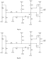
- Fig. 4a is a schematic diagram of an equivalent circuit of the shift register shown in Fig. 2 when the shift register operates in the output preparation stage, and as shown in Fig. 4a , the third transistor M3, the fourth transistor M4, the fifth transistor M5, the seventh transistor M7, the eighth transistor M8, and the eleventh transistor M11 are all turned on, and the second transistor M2, the sixth transistor M6, the twelfth transistor M12, the ninth transistor M9, the tenth transistor M10, the thirteenth transistor M13, and the fourteenth transistor M14 are all turned off.
- the third transistor M3 and the fourth transistor M4 are turned on, and at this time, the first operating voltage VGL1 is written into the control electrode of the second transistor M2 through the third transistor M3, the second transistor M2 is in an off-state, and the first transistor M1 is equivalent to one resistor.
- the third operating voltage VGL2 can be written into the second node N2 through the fourth transistor M4 and the fifth transistor M5 in sequence, the voltage at the second node N2 is in a low level state, and the sixth transistor M6, the tenth transistor M10 and the fourteenth transistor M14 are all turned off.
- the second operating voltage VGH1 is written into the third node N3 through the seventh transistor M7, the voltage at the third node N3 is in a high level state, the eighth transistor M8 and the eleventh transistor M11 are in an on-state, and the first clock signal in a low level state is written into the second terminal of the first capacitor C1 through the eighth transistor M8. Meanwhile, since the first clock signal is in a low level state, the ninth transistor M9 and the twelfth transistor M12 are turned off.
- the ninth transistor M9 and the tenth transistor M10 are turned off, the first node N1 is in a floating state, i.e., the voltage at the first node N1 is maintained in the previous low level state, and the thirteenth transistor M13 is turned off. Since both the thirteenth transistor M13 and the fourteenth transistor M14 are turned off, the voltage at the signal output terminal OUT is maintained in the previous low level state.
- the continuous-output stage t2 includes at least one continuous-output period including one first output sub-stage t201 and one second output sub-stage t202; the case where the continuous-output stage t2 includes only one continuous-output period is exemplarily illustrated in Fig. 3 , i.e., the entire continuous-output stage t2 includes only one first output sub-stage t201 and one second output sub-stage t202.
- the input signal provided by the signal input terminal STU is in a high level state
- the first clock signal provided by the first clock signal terminal CLK1 is in a high level state
- the second clock signal provided by the second clock signal terminal CLK2 is in a low level state.
- Fig. 4b is a schematic diagram of an equivalent circuit of the shift register shown in Fig. 2 when the shift register operates in the first output sub-stage, and as shown in Fig. 4b , the third transistor M3, the fourth transistor M4, the eighth transistor M8, the ninth transistor M9, the eleventh transistor M11, the twelfth transistor M12, and the thirteenth transistor M13 are all turned on, and the second transistor M2, the fifth transistor M5, the sixth transistor M6, the seventh transistor M7, the tenth transistor M10, and the fourteenth transistor M14 are all turned off.
- the third transistor M3 and the fourth transistor M4 are turned on, and at this time, the first operating voltage VGL1 is written into the control electrode of the second transistor M2 through the third transistor M3, the second transistor M2 is in an off-state, and the first transistor M1 is equivalent to one resistor.
- the fifth transistor M5 and the seventh transistor M7 are turned off.
- the sixth transistor M6 is maintained in the off-state, the third node N3 is in a floating state, and the eighth transistor M8 and the eleventh transistor M11 are maintained in an on-state.
- the ninth transistor M9 and the twelfth transistor M12 are turned on.
- the third operating voltage VGL2 is written into the second node N2 through the eleventh transistor M11 and the twelfth transistor M12, so as to maintain the second node N2 in a low level state all the time, thereby achieving the purpose of reducing noise for the second node N2.
- the eighth transistor M8 and the ninth transistor M9 are turned on, the first clock signal in a high level state is written into the second terminal of the first capacitor C1 through the eighth transistor M8, and is written into the first node N1 through the ninth transistor M9, and the voltage at the first node N1 is in a high level state.
- the first clock signal is switched from a low level state to a high level state, the voltage at the second terminal of the first capacitor C1 is charged from a low level state to a high level state, and since the third node N3 is in a floating state, the voltage at the third node N3 is pulled up to a higher level under the bootstrap effect of the first capacitor C1; and at the end of the first output sub-stage t201, the first clock signal is switched from a high level state to a low level state, and the voltage at the second terminal of the first capacitor C1 is discharged from a high level state to a low level state, so that the voltage at the third node N3 is restored to the original level (which is still in a high level state but has a decreased voltage level) under the bootstrap effect of the first capacitor C1.
- the thirteenth transistor M13 is turned on, the fourteenth transistor M14 is turned off, the second operating voltage VGH1 is written into the signal output terminal OUT through the thirteenth transistor M13, and the signal output terminal OUT outputs a high level signal.
- the input signal provided by the signal input terminal STU is in a high level state
- the first clock signal provided by the first clock signal terminal CLK1 is in a low level state
- the second clock signal provided by the second clock signal terminal CLK2 is in a high level state.
- Fig. 4c is a schematic diagram of an equivalent circuit of the shift register shown in Fig. 2 when the shift register operates in the second output sub-stage, and as shown in Fig. 4c , the third transistor M3, the fourth transistor M4, the fifth transistor M5, the seventh transistor M7, the eighth transistor M8, the eleventh transistor M11, and the thirteenth transistor M13 are all turned on, and the second transistor M2, the sixth transistor M6, the ninth transistor M9, the tenth transistor M10, the twelfth transistor M12, and the fourteenth transistor M14 are all turned off.
- the third transistor M3 and the fourth transistor M4 are turned on, and at this time, the first operating voltage VGL1 is written into the control electrode of the second transistor M2 through the third transistor M3, the second transistor M2 is in an off-state, and the first transistor M1 is equivalent to one resistor.
- the third operating voltage VGL2 can be written into the second node N2 through the fourth transistor M4 and the fifth transistor M5 in sequence, the voltage at the second node N2 is maintained in the low level state, and the sixth transistor M6, the tenth transistor M10 and the fourteenth transistor M14 are all turned off.
- the second operating voltage VGH1 is written into the third node N3 through the seventh transistor M7, the voltage at the third node N3 is in a high level state, the eighth transistor M8 and the eleventh transistor M11 are in an on-state, and the first clock signal in a low level state is written into the second terminal of the first capacitor C1 through the eighth transistor M8.
- the ninth transistor M9 and the twelfth transistor M12 are turned off. Since both the ninth transistor M9 and the tenth transistor M10 are turned off, the first node N1 is in a floating state, and the voltage at the first node N1 is maintained in the previous high level state.
- the thirteenth transistor M13 is turned on, the fourteenth transistor M14 is turned off, the second operating voltage VGH1 is written into the signal output terminal OUT through the thirteenth transistor M13, and the signal output terminal OUT continuously outputs a high level signal.
- the input signal provided by the signal input terminal STU is in a low level state
- the first clock signal provided by the first clock signal terminal CLK1 is in a high level state
- the second clock signal provided by the second clock signal terminal CLK2 is in a low level state.
- Fig. 4d is a schematic diagram of an equivalent circuit of the shift register shown in Fig. 2 when the shift register operates in the final output stage, and as shown in Fig. 4d , the second transistor M2, the eighth transistor M8, the ninth transistor M9, the eleventh transistor M11, the twelfth transistor M12, and the thirteenth transistor M13 are all turned on, and the third transistor M3, the fourth transistor M4, the fifth transistor M5, the sixth transistor M6, the seventh transistor M7, the tenth transistor M10, and the fourteenth transistor M14 are all turned off.
- the third transistor M3 and the fourth transistor M4 are turned off, and at this time, the second operating voltage VGH1 is written into the control electrode of the second transistor M2 through the first transistor M1, the second transistor M2 is in an on-state, and the second operating voltage VGH1 is written into the first electrode of the fifth transistor M5 through the second transistor M2.
- the fifth transistor M5 and the seventh transistor M7 are turned off.
- the sixth transistor M6 is maintained in a low level state
- the third node N3 is in a floating state
- the eighth transistor M8 and the eleventh transistor M11 are maintained in an on-state.
- the ninth transistor M9 and the twelfth transistor M12 are turned on.
- the third operating voltage VGL2 is written into the second node N2 through the eleventh transistor M11 and the twelfth transistor M12, so as to maintain the second node N2 in a low level state all the time, thereby achieving the purpose of reducing noise for the second node N2.
- the eighth transistor M8 and the ninth transistor M9 are turned on, the first clock signal in a high level state is written into the second terminal of the first capacitor C1 through the eighth transistor M8, and is written into the first node N1 through the ninth transistor M9, and the voltage at the first node N1 is in a high level state.
- the first clock signal is switched from a low level state to a high level state, the voltage at the second terminal of the first capacitor C1 is charged from a low level state to a high level state, and since the third node N3 is in a floating state, the voltage at the third node N3 is pulled up to a higher level under the bootstrap effect of the first capacitor C1; and at the end of the final output stage t3, the first clock signal is switched from a high level state to a low level state, and the voltage at the second terminal of the first capacitor C1 is discharged from a high level state to a low level state, so that the voltage at the third node N3 is restored to the original level (which is still in a high level state but has a decreased level) under the bootstrap effect of the first capacitor C1.
- the thirteenth transistor M13 is turned on, the fourteenth transistor M14 is turned off, the second operating voltage VGH1 is written into the signal output terminal OUT through the thirteenth transistor M13, and the signal output terminal OUT continuously outputs a high level signal.
- the voltage at the first node N1 is maintained in a high level state
- the voltage at the second node N2 is maintained in a low level state
- the signal output terminal OUT continuously outputs a high level signal.
- the input signal provided by the signal input terminal STU is in a low level state
- the first clock signal provided by the first clock signal terminal CLK1 is in a low level state
- the second clock signal provided by the second clock signal terminal CLK2 is in a high level state.
- Fig. 4e is a schematic diagram of an equivalent circuit of the shift register shown in Fig. 2 when the shift register operates in the reset stage, and as shown in Fig. 4e , the second transistor M2, the fifth transistor M5, the sixth transistor M6, the seventh transistor M7, the eighth transistor M8, the tenth transistor M10, the eleventh transistor M11, and the fourteenth transistor M14 are all turned on, and the third transistor M3, the fourth transistor M4, the ninth transistor M9, the twelfth transistor M12, and the thirteenth transistor M13 are all turned off.
- the third transistor M3 and the fourth transistor M4 are turned off, and at this time, the second operating voltage VGH1 is written into the control electrode of the second transistor M2 through the first transistor M1, the second transistor M2 is in an on-state, and the second operating voltage VGH1 is written into the first electrode of the fifth transistor M5 through the second transistor M2.
- the second operating voltage VGH1 can be written into the second node N2 through the second transistor M2 and the fifth transistor M5 in sequence, the voltage at the second node N2 is in a high level state, at this time, the sixth transistor M6 is turned on, the second clock signal in a high level state is written into the third node N3 through the sixth transistor M6, the second operating voltage VGH1 is written into the third node N3 through the seventh transistor M7, the voltage at the third node N3 is in a high level state, and the eighth transistor M8 and the eleventh transistor M11 are turned on.
- the first operating voltage VGL1 is written into the first node N1 through the tenth transistor M10, and the voltage at the first node N1 is in a low level state; meanwhile, since the first clock signal is in a low level state, the ninth transistor M9 and the twelfth transistor M12 are in an off-state.
- the thirteenth transistor M13 is turned off, and the fourteenth transistor M14 is turned on, the first operating voltage VGL is written into the signal output terminal OUT through the fourteenth transistor M14, and the signal output terminal OUT outputs a low level signal.
- the second clock signal is switched from a high level state to a low level state, and the sixth transistor M6 is maintained in an on-state, so that the second clock signal in a low level state is written into the third node N3 through the sixth transistor M6, and the voltage at the third node N3 is in a low level state.
- a holding stage t5 may be further included, in which the input signal provided by the signal input terminal STU is in a low level state, the first clock signal provided by the first clock signal terminal CLK1 is in a high level state, and the second clock signal provided by the second clock signal terminal CLK2 is in a low level state.
- Fig. 4f is a schematic diagram of an equivalent circuit of the shift register shown in Fig. 2 when the shift register operates in the holding stage, and as shown in Fig. 4f , the second transistor M2, the sixth transistor M6, the ninth transistor M9, the tenth transistor M10, the twelfth transistor M12 and the fourteenth transistor M14 are all turned on, and the third transistor M3, the fourth transistor M4, the fifth transistor M5, the seventh transistor M7, the eighth transistor M8, the tenth transistor M10, the eleventh transistor M11 and the thirteenth transistor M13 are all turned off.
- the third transistor M3 and the fourth transistor M4 are turned off, and at this time, the second operating voltage VGH1 is written into the control electrode of the second transistor M2 through the first transistor M1, the second transistor M2 is in an on-state, and the second operating voltage VGH1 is written into the first electrode of the fifth transistor M5 through the second transistor M2.
- the fifth transistor M5 and the seventh transistor M7 are turned off.
- the second node N2 is maintained in the previous high level state
- the sixth transistor M6 and the tenth transistor M10 are turned on
- the second clock signal in a low level state is written into the second node N2 through the sixth transistor M6 to maintain the second node N2 in a low level state
- the eighth transistor M8 and the eleventh transistor M11 are turned off.
- the ninth transistor M9 and the twelfth transistor M12 are turned on. Since the tenth transistor M10 is turned on, the first operating voltage VGL1 is written into the first node N1 through the tenth transistor M10, and the first node N1 is in a low level state.
- the thirteenth transistor M13 is turned off, the fourteenth transistor M14 is turned on, the first operating voltage VGL is written into the signal output terminal OUT through the fourteenth transistor M14, and the signal output terminal OUT outputs a low level signal.
- the reset stage t4 and the holding stage t5 are alternated until the next operating cycle starts; and in this process, the voltage at the first node N1 is continuously in a low level state, the voltage at the second node N2 is continuously in a high level state, the voltage at the third node N3 is in a high level state in the reset stage t4 but is in a low level state at the end of the reset stage t4, and the output terminal continuously outputs a low level signal.
- Fig. 5 is another timing diagram illustrating an operation of the shift register shown in Fig. 2 , and as shown in Fig. 5 , unlike the operation timing shown in Fig. 3 , the duration in which the input signal is in an active level state in Fig. 5 is increased by T, which is the period of the first or second clock signal, compared with the duration in which the input signal is in an active level state in Fig. 3 .
- the continuous-output stage t2 includes two continuous-output periods, i.e. the entire continuous-output stage t2 includes two first output sub-stages t201 and two second output sub-stages t 202.
- the duration in which the scan driving signal output from the signal output terminal OUT is in an active level state in Fig. 5 is increased by T compared with the duration in which the input signal is in an active level state in Fig. 3 .
- Fig. 6 is another timing diagram illustrating an operation of the shift register shown in Fig. 2 , and as shown in Fig. 6 , unlike the operation timing shown in Fig. 3 , the duration in which the input signal is in an active level state in Fig. 6 is increased by 2T, where T is the period of the first or second clock signal, compared with the duration in which the input signal is in an active level state in Fig. 3 .
- the continuous-output stage t2 includes three continuous-output periods, i.e., the entire continuous-output stage t2 includes three first output sub-stages t201 and three second output sub-stages t202.
- the duration in which the scan driving signal output from the signal output terminal OUT is in an active level state in Fig. 6 is increased by 2T compared with the duration in which the input signal is in an active level state in Fig. 3 .
- the continuous-output stage t2 includes more than three continuous-output periods, no further example is described here; it should be noted that, in the embodiment of the present disclosure, in each operating cycle, it should be ensured that the time when the input signal is switched from an inactive state to an active level state (i.e., the rising edge in the example) is aligned with the time when the second clock signal is switched from an inactive state to an active level state (i.e., the rising edge in the example); and the time when the input signal is switched from an active level state to an inactive level state (i.e., the falling edge in the example) is aligned with the time when the first clock signal is switched from an inactive state to an active level state (i.e., the rising edge in the example).
- an active level state i.e., the rising edge in the example
- the pulse width of the scan driving signal provided to the gate line by the shift register is adjustable, so that the change of the internal compensation time of the pixel circuit can be adapted.
- all transistors in the shift register may also be P-type transistors, and in this case, the operating process of the shift register is the same as that of the shift register in which the transistors are N-type transistors, which is not described herein again.
- Fig. 7 is a schematic circuit diagram of a gate driving circuit according to an embodiment of the present disclosure, and as shown in Fig. 7 , the gate driving circuit includes a plurality of cascaded shift registers SR_1, SR_2, SR_3 and SR_4, where the shift registers SR_1, SR_2, SR_3 and SR_4 adopt the shift registers provided by the above embodiment.
- the signal input terminal STU of the shift register SR_2, SR_3, or SR_4 is coupled to the signal output terminal OUT of the previous stage of shift register.
- Fig. 7 only shows the first four stages of shift registers by way of example.
- two clock signal supply lines are provided for the gate driving circuit: a first clock signal supply line CK1 and a second clock signal supply line CK 2.
- the odd-numbered stages of shift registers SR_1 and SR_3 have their first clock signal terminals CLK1 coupled to the first clock signal supply line CK1 and their second clock signal terminals CLK2 coupled to the second clock signal supply line CK 2; and the even-numbered stages of shift registers SR_2 and SR_4 have their first clock signal terminals CLK1 coupled to the second clock signal supply line CK2 and their second clock signal terminals CLK2 coupled to the first clock signal supply line CK 1.
- each stage of shift register in the gate driving circuit is configured with a signal input terminal and a reset signal terminal; and the reset signal terminal is coupled with control electrodes of transistors in the shift register and is configured to control the reset process on the voltages at the first node/the second node in the shift register.
- the reset signal terminal of the current stage of shift register is coupled to the signal output terminal of the next stage of shift register.
- two signal lines are required to be disposed in each stage of shift registers except for the first and last stages of shift registers, where one signal line is configured to couple the signal input terminal STU of the current stage of shift register and the signal output terminal of the previous stage of shift register, and the other signal line is configured to couple the reset signal terminal of the current stage of shift register and the signal output terminal of the next stage of shift register.
- the reset process on the voltages at the first node N1/the second node N2 in each stage of the shift registers is controlled by the first clock signal terminal CLK1 and the second clock signal terminal CLK2, and the shift registers do not need to be configured with the reset signal terminal, so that each stage of the shift register except for the first and last stages of shift registers only needs to be configured with one signal line for coupling the signal input terminal STU of the current stage of shift register and the signal output terminal OUT of the previous stage of shift register.
- the embodiment of the present disclosure can effectively reduce the number of signal lines, thereby reducing the overall size of the gate driving circuit and being beneficial to the narrow bezel design of the display device.
- Fig. 8 is a flowchart illustrating a gate driving method according to an embodiment of the present disclosure, and as shown in Fig. 8 , the gate driving method is based on the shift register provided in the above embodiment, and the gate driving method includes steps S1 to S4.
- step S1 in the output preparation stage, the signal writing circuit inverts the input signal in an active level state in response to a control of the second clock signal, and writes the generated inverted signal in an inactive level state into the second node, and the voltage control circuit writes the second operating voltage into the third node in response to the control of the second clock signal.
- Step S2 corresponds to the continuous-output stage, and includes step S201 and step S202.
- the continuous-output stage includes at least one continuous-output period, and the continuous-output period includes a first output sub-stage and a second output sub-stage.
- step S201 in the first output sub-stage, the voltage control circuit writes the first clock signal in an active level state into the first node in response to the control of the voltage at the third node and the first clock signal, and the output circuit writes the second operating voltage into the signal output terminal in response to the control of the voltage at the first node.
- step S202 in the second output sub-stage, the signal writing circuit inverts the input signal in an active level state in response to the control of the second clock signal, and writes the generated inverted signal in an inactive level state into the second node, where the first node is in a floating state and the voltage at the first node is maintained in an active level state.
- step S3 in the final output stage, the voltage control circuit writes the first clock signal in an active level state into the first node in response to the control of the voltage at the third node and the first clock signal, and the output circuit writes the second operating voltage into the signal output terminal in response to the control of the voltage at the first node.
- step S4 in the reset stage, the signal writing circuit inverts the input signal in an inactive level state in response to the control of the second clock signal, and writes the generated inverted signal in an active level state into the second node, the voltage control circuit writes the first operating voltage into the first node in response to the control of the voltage at the second node, and the output circuit writes the first operating voltage into the signal output terminal in response to the control of the voltage at the second node.
Landscapes
- Engineering & Computer Science (AREA)
- Physics & Mathematics (AREA)
- Computer Hardware Design (AREA)
- General Physics & Mathematics (AREA)
- Theoretical Computer Science (AREA)
- Control Of Indicators Other Than Cathode Ray Tubes (AREA)
- Shift Register Type Memory (AREA)
- Liquid Crystal Display Device Control (AREA)
Claims (10)
- Schieberegister, eine Signalschreibschaltung (1), eine Spannungssteuerschaltung (2) und eine Ausgabeschaltung (3) aufweisend, wobei die Spannungssteuerschaltung (2) und die Ausgabeschaltung (3) mit einem ersten Knoten (N1) gekoppelt sind und die Signalschreibschaltung (1), die Spannungssteuerschaltung (2) und die Ausgabeschaltung (3) mit einem zweiten Knoten (N2) gekoppelt sind, wobeidie Signalschreibschaltung (1) konfiguriert ist, um ein invertiertes Signal eines Eingabesignals, das von einem Signaleingabeanschluss (STU) vorgesehen wird, als Reaktion auf eine Steuerung eines zweiten Taktsignals, das von einem zweiten Taktsignalanschluss (CLK2) vorgesehen wird, in den zweiten Knoten (N2) zu schreiben;die Spannungssteuerschaltung (2) eine erste Steuerschaltung (201) und eine zweite Steuerschaltung (202) aufweist, die erste Steuerschaltung (201) einen sechsten Transistor (M6) und einen siebten Transistor (M7) aufweist, eine Steuerelektrode des sechsten Transistors mit dem zweiten Knoten (N2) gekoppelt ist, eine erste Elektrode des sechsten Transistors (M6) mit dem zweiten Taktsignalanschluss (CLK2) gekoppelt ist und eine zweite Elektrode des sechsten Transistors (M6) mit einem dritten Knoten (N3) gekoppelt ist, eine Steuerelektrode des siebten Transistors (M7) mit dem zweiten Taktsignalanschluss (CLK2) gekoppelt ist, eine erste Elektrode des siebten Transistors (M7) mit dem dritten Knoten (N3) gekoppelt ist und eine zweite Elektrode des siebten Transistors (M7) mit einem zweiten Stromversorgungsanschluss (VGH1) gekoppelt ist, die zweite Steuerschaltung (202) einen ersten Kondensator (C1), einen achten Transistor (M8), einen neunten Transistor (M9) und einen zehnten Transistor (M10) aufweist, ein erster Anschluss des ersten Kondensators (C1) mit einer Steuerelektrode des achten Transistors (M8) und dem dritten Knoten (N3) gekoppelt ist und ein zweiter Anschluss des ersten Kondensators (C1) mit der ersten Elektrode des achten Transistors (M8) und einer zweiten Elektrode des neunten Transistors gekoppelt ist, eine zweite Elektrode des achten Transistors (M8) mit einem ersten Taktsignalanschluss (CLK1) gekoppelt ist, eine Steuerelektrode des neunten Transistors (M9) mit dem ersten Taktsignalanschluss (CLK1) gekoppelt ist und eine erste Elektrode des neunten Transistors (M9) mit dem ersten Knoten (N1) gekoppelt ist, eine Steuerelektrode des zehnten Transistors (M10) mit dem zweiten Knoten (N2) gekoppelt ist und eine erste Elektrode des zehnten Transistors (M10) mit einem ersten Stromversorgungsanschluss (VGL1) gekoppelt ist, der zweite Stromversorgungsanschluss eine Spannung mit aktivem Pegel liefert und der erste Stromversorgungsanschluss eine Spannung mit inaktivem Pegel liefert; unddie Ausgabeschaltung (3) einen dreizehnten Transistor (M13) und einen vierzehnten Transistor (M14) aufweist, eine Steuerelektrode des dreizehnten Transistors (M13) mit dem ersten Knoten (N1) gekoppelt ist, eine erste Elektrode des dreizehnten Transistors (M13) mit dem zweiten Stromversorgungsanschluss gekoppelt ist und eine zweite Elektrode des dreizehnten Transistors (M13) mit einem Signalausgabeanschluss (OUT) gekoppelt ist, eine Steuerelektrode des vierzehnten Transistors (M14) mit dem zweiten Knoten (N2) gekoppelt ist, eine erste Elektrode des vierzehnten Transistors (M14) mit dem Signalausgabeanschluss (OUT) gekoppelt ist und eine zweite Elektrode des vierzehnten Transistors (M14) mit dem ersten Stromversorgungsanschluss (VGL1) gekoppelt ist.
- Schieberegister nach Anspruch 1, wobei die Signalschreibschaltung (1) eine Inverterschaltung (101) und eine Schreibsteuerschaltung (102) aufweist;die Inverterschaltung (101) mit dem Signaleingabeanschluss (STU) gekoppelt ist und konfiguriert ist, um das Eingabesignal, das von dem Signaleingabeanschluss (STU) vorgesehen wird, zu invertieren und das invertierte Signal über einen Ausgabeanschluss der Inverterschaltung (101) auszugeben; unddie Schreibsteuerschaltung (102) mit der Inverterschaltung (101) gekoppelt ist und konfiguriert ist, um das invertierte Signal als Reaktion auf die Steuerung des zweiten Taktsignals in den zweiten Knoten (N2) zu schreiben.
- Schieberegister nach Anspruch 2, wobei die Inverterschaltung (101) einen ersten Transistor (M1), einen zweiten Transistor (M2), einen dritten Transistor (M3) und einen vierten Transistor (M4) aufweist;eine Steuerelektrode und eine erste Elektrode des ersten Transistors (M1) mit dem zweiten Stromversorgungsanschluss (VGH1) gekoppelt sind und eine zweite Elektrode des ersten Transistors (M1) mit einer Steuerelektrode des zweiten Transistors (M2) und einer ersten Elektrode des dritten Transistors (M3) gekoppelt ist;eine erste Elektrode des zweiten Transistors (M2) mit dem zweiten Stromversorgungsanschluss gekoppelt ist und eine zweite Elektrode des zweiten Transistors (M2) mit einer ersten Elektrode des vierten Transistors (M4) gekoppelt ist;eine Steuerelektrode des dritten Transistors (M3) mit dem Signaleingabeanschluss (STU) gekoppelt ist und eine zweite Elektrode des dritten Transistors (M3) mit dem ersten Stromversorgungsanschluss gekoppelt ist; undeine Steuerelektrode des vierten Transistors (M4) mit dem Signaleingabeanschluss (STU) gekoppelt ist, eine erste Elektrode des vierten Transistors (M4) mit der Schreibsteuerschaltung (102) gekoppelt ist und eine zweite Elektrode des vierten Transistors (M4) mit einem dritten Stromversorgungsanschluss (VGL2) gekoppelt ist.
- Schieberegister nach Anspruch 2, wobei die Schreibsteuerschaltung (102) einen fünften Transistor (M5) aufweist;
eine Steuerelektrode des fünften Transistors (M5) mit dem zweiten Taktsignalanschluss (CLK2) gekoppelt ist, eine erste Elektrode des fünften Transistors (M5) mit dem Ausgabeanschluss der Inverterschaltung (101) gekoppelt ist und eine zweite Elektrode des fünften Transistors (M5) mit dem zweiten Knoten (N2) gekoppelt ist. - Schieberegister nach Anspruch 1, ferner eine Reglerschaltung (4) aufweisend, wobei
die Reglerschaltung (4) mit dem zweiten Knoten (N2) und dem dritten Knoten (N3) gekoppelt ist und konfiguriert ist, um als Reaktion auf die Steuerung der Spannung an dem dritten Knoten (N3) und dem ersten Taktsignal eine dritte Betriebsspannung, die von einem dritten Stromversorgungsanschluss vorgesehen wird, in den zweiten Knoten (N2) zu schreiben. - Schieberegister nach Anspruch 5, wobei die Reglerschaltung (4) einen elften Transistor (M11) und einen zwölften Transistor (M12) aufweist;eine Steuerelektrode des elften Transistors (M11) mit dem dritten Knoten (N3) gekoppelt ist, eine erste Elektrode des elften Transistors (M11) mit dem dritten Stromversorgungsanschluss (VGL2) gekoppelt ist und eine zweite Elektrode des elften Transistors (M11) mit einer ersten Elektrode des zwölften Transistors (M12) gekoppelt ist; undeine Steuerelektrode des zwölften Transistors (M12) mit dem ersten Taktsignalanschluss (CLK1) gekoppelt ist und eine zweite Elektrode des zwölften Transistors (M12) mit dem zweiten Knoten (N2) gekoppelt ist.
- Schieberegister nach Anspruch 6, wobei die Ausgabeschaltung (3) ferner einen zweiten Kondensator (C2) und einen dritten Kondensator (C3) aufweist;ein erster Anschluss des zweiten Kondensators (C2) mit dem ersten Knoten (N1) gekoppelt ist und ein zweiter Anschluss des zweiten Kondensators (C2) mit dem zweiten Stromversorgungsanschluss (VGH1) gekoppelt ist; undein erster Anschluss des dritten Kondensators (C3) mit dem zweiten Knoten (N2) gekoppelt ist und ein zweiter Anschluss des dritten Kondensators (C3) mit dem ersten Stromversorgungsanschluss (VGL1) gekoppelt ist.
- Schieberegister nach einem der Ansprüche 1 bis 7, wobei sämtliche Transistoren in dem Schieberegister n-Typ-Transistoren sind; oder
alle Transistoren in dem Schieberegister p-Typ-Transistoren sind. - Gate-Ansteuerschaltung, aufweisend:mehrere kaskadierte Schieberegister, wobei jedes der mehreren kaskadierten Schieberegister das Schieberegister nach einem der Ansprüche 1 bis 8 ist,wobei der Signaleingabeanschluss (STU) jeder anderen Stufe von Schieberegistern als einer ersten Stufe von Schieberegistern unter den mehreren kaskadierten Schieberegistern mit dem Signalausgabeanschluss einer vorherigen Stufe von Schieberegistern gekoppelt ist.
- Gate-Ansteuerverfahren, wobei das Gate-Ansteuerverfahren auf dem Schieberegister nach einem der Ansprüche 1 bis 8 basiert und das Gate-Ansteuerverfahren umfasst:in einer Ausgabevorbereitungsstufe, als Reaktion auf die Steuerung des zweiten Taktsignals Invertieren des Eingabesignals in einem aktiven Pegelzustand durch die Signalschreibschaltung (1), Schreiben eines erzeugten invertierten Signals in einen inaktiven Pegelzustand in den zweiten Knoten (N2) durch die Signalschreibschaltung (1) und als Reaktion auf die Steuerung des zweiten Taktsignals Schreiben der zweiten Betriebsspannung in den dritten Knoten (N3) durch die Spannungssteuerschaltung (2);in einer Stufe kontinuierlicher Ausgabe, die mindestens eine Periode kontinuierlicher Ausgabe aufweist, die eine erste Ausgabe-Teilstufe und eine zweite Ausgabe-Teilstufe aufweist,in der ersten Ausgabe-Teilstufe, als Reaktion auf die Steuerung der Spannung an dem dritten Knoten (N3) und des ersten Taktsignals Schreiben des ersten Taktsignals in einem aktiven Pegelzustand in den ersten Knoten (N1) durch die Spannungssteuerschaltung (2) und als Reaktion auf die Steuerung der Spannung an dem ersten Knoten Schreiben der zweiten Betriebsspannung in den Signalausgabeanschluss durch die Ausgabeschaltung (3) ;in der zweiten Ausgabe-Teilstufe, als Reaktion auf die Steuerung des zweiten Taktsignals Invertieren des Eingabesignals in einem aktiven Pegelzustand durch die Signalschreibschaltung (1) und Schreiben eines erzeugten invertierten Signals in einem inaktiven Pegelzustand in den zweiten Knoten (N2) durch die Signalschreibschaltung (1), wobei sich der erste Knoten in einem schwebenden Zustand befindet und die Spannung an dem ersten Knoten in einem aktiven Pegelzustand gehalten wird;in einer abschließenden Ausgabestufe, als Reaktion auf die Steuerung der Spannung an dem dritten Knoten und des ersten Taktsignals Schreiben des ersten Taktsignals in einem aktiven Pegelzustand in den ersten Knoten durch die Spannungssteuerschaltung (2) und als Reaktion auf die Steuerung der Spannung an dem ersten Knoten Schreiben der zweiten Betriebsspannung in den Signalausgabeanschluss durch die Ausgabeschaltung (3); undin einer Rücksetzstufe, als Reaktion auf die Steuerung des zweiten Taktsignals Invertieren des Eingabesignals in einem inaktiven Pegelzustand durch die Signalschreibschaltung (1) und Schreiben eines erzeugten invertierten Signals in einem aktiven Pegelzustand in den zweiten Knoten (N2) durch die Signalschreibschaltung (1), als Reaktion auf die Steuerung der Spannung an dem zweiten Knotenpunkt (N2) Schreiben der ersten Betriebsspannung in den ersten Knotenpunkt durch die Spannungssteuerschaltung (2) und als Reaktion auf die Steuerung der Spannung an dem zweiten Knotenpunkt (N2) Schreiben der ersten Betriebsspannung in den Signalausgabeanschluss durch die Ausgabeschaltung (3).
Applications Claiming Priority (1)
| Application Number | Priority Date | Filing Date | Title |
|---|---|---|---|
| PCT/CN2020/087988 WO2021217548A1 (zh) | 2020-04-30 | 2020-04-30 | 移位寄存器、栅极驱动电路和栅极驱动方法 |
Publications (3)
| Publication Number | Publication Date |
|---|---|
| EP4145433A1 EP4145433A1 (de) | 2023-03-08 |
| EP4145433A4 EP4145433A4 (de) | 2023-05-24 |
| EP4145433B1 true EP4145433B1 (de) | 2025-03-19 |
Family
ID=78293183
Family Applications (1)
| Application Number | Title | Priority Date | Filing Date |
|---|---|---|---|
| EP20926355.7A Active EP4145433B1 (de) | 2020-04-30 | 2020-04-30 | Schieberegister, treiberschaltung für gate-elektroden und ansteuerverfahren für gate-elektroden |
Country Status (4)
| Country | Link |
|---|---|
| US (1) | US11328785B2 (de) |
| EP (1) | EP4145433B1 (de) |
| CN (1) | CN114097020B (de) |
| WO (1) | WO2021217548A1 (de) |
Families Citing this family (2)
| Publication number | Priority date | Publication date | Assignee | Title |
|---|---|---|---|---|
| DE112022007615T5 (de) | 2022-05-26 | 2025-05-22 | Boe Technology Group Co. Ltd. | Schieberegistereinheit, treibersteuerschaltung, anzeigevorrichtung und treiberverfahren |
| CN116959358B (zh) * | 2023-08-01 | 2026-03-13 | 京东方科技集团股份有限公司 | 移位寄存器、栅极驱动电路、阵列基板及显示装置 |
Family Cites Families (23)
| Publication number | Priority date | Publication date | Assignee | Title |
|---|---|---|---|---|
| US20040150449A1 (en) * | 2003-01-30 | 2004-08-05 | Sun Microsystems, Inc. | High-speed flip-flop circuitry and method for operating the same |
| AU2007254173B2 (en) * | 2006-05-17 | 2013-07-25 | Nuvasive, Inc. | Surgical trajectory monitoring system and related methods |
| CN101604551B (zh) * | 2008-06-10 | 2012-05-30 | 北京京东方光电科技有限公司 | 移位寄存器及其栅线驱动装置 |
| KR101975581B1 (ko) * | 2012-08-21 | 2019-09-11 | 삼성디스플레이 주식회사 | 발광 제어 구동부 및 그것을 포함하는 유기발광 표시장치 |
| TWI500265B (zh) * | 2012-11-22 | 2015-09-11 | Au Optronics Corp | 移位暫存器 |
| CN104700801B (zh) * | 2015-03-24 | 2016-11-02 | 深圳市华星光电技术有限公司 | Pmos栅极驱动电路 |
| KR102413874B1 (ko) * | 2015-07-02 | 2022-06-29 | 삼성디스플레이 주식회사 | 발광제어 구동부 및 이를 포함하는 표시장치 |
| CN105185287B (zh) * | 2015-08-27 | 2017-10-31 | 京东方科技集团股份有限公司 | 一种移位寄存器、栅极驱动电路和相关显示装置 |
| CN105047124B (zh) * | 2015-09-18 | 2017-11-17 | 京东方科技集团股份有限公司 | 一种移位寄存器、栅极驱动电路及显示装置 |
| KR102431435B1 (ko) * | 2015-10-26 | 2022-08-12 | 삼성디스플레이 주식회사 | 발광제어 구동부 및 이를 포함하는 표시 장치 |
| CN105741802B (zh) * | 2016-03-28 | 2018-01-30 | 京东方科技集团股份有限公司 | 移位寄存器单元及其驱动方法、栅极驱动电路、显示装置 |
| KR102582032B1 (ko) * | 2016-04-05 | 2023-09-25 | 삼성디스플레이 주식회사 | 발광 구동부 및 이를 포함하는 표시 장치 |
| KR102463953B1 (ko) * | 2016-05-25 | 2022-11-08 | 삼성디스플레이 주식회사 | 발광 제어 구동부 및 이를 포함하는 표시 장치 |
| CN106057143A (zh) * | 2016-05-30 | 2016-10-26 | 京东方科技集团股份有限公司 | 移位寄存器及其操作方法、栅极驱动电路和显示装置 |
| CN106887209B (zh) * | 2017-04-28 | 2019-04-16 | 京东方科技集团股份有限公司 | 移位寄存器单元及其驱动方法、移位寄存器以及显示装置 |
| CN107316599B (zh) * | 2017-07-07 | 2020-09-22 | 上海天马有机发光显示技术有限公司 | 移位寄存单元、其驱动方法及显示面板 |
| KR102428732B1 (ko) * | 2017-12-27 | 2022-08-02 | 엘지디스플레이 주식회사 | 스캔 구동부와 이를 포함한 표시장치 |
| CN107978265B (zh) * | 2018-01-22 | 2021-01-26 | 京东方科技集团股份有限公司 | 移位寄存器单元、驱动方法、栅极驱动电路及显示装置 |
| CN108806583B (zh) * | 2018-07-05 | 2020-12-01 | 京东方科技集团股份有限公司 | 移位寄存器单元、驱动方法、移位寄存器和显示装置 |
| KR102498797B1 (ko) * | 2018-09-28 | 2023-02-10 | 삼성디스플레이 주식회사 | 유기 발광 표시 장치 |
| KR102712567B1 (ko) * | 2018-11-30 | 2024-10-07 | 삼성디스플레이 주식회사 | 주사 구동부 |
| CN110189676B (zh) * | 2019-05-31 | 2021-04-02 | 京东方科技集团股份有限公司 | 移位寄存器单元及驱动方法、栅极驱动电路、显示面板 |
| CN110491329B (zh) * | 2019-09-25 | 2023-02-17 | 京东方科技集团股份有限公司 | 移位寄存器及其驱动方法、栅极驱动电路和显示装置 |
-
2020
- 2020-04-30 CN CN202080000625.1A patent/CN114097020B/zh active Active
- 2020-04-30 EP EP20926355.7A patent/EP4145433B1/de active Active
- 2020-04-30 WO PCT/CN2020/087988 patent/WO2021217548A1/zh not_active Ceased
- 2020-11-25 US US17/104,809 patent/US11328785B2/en active Active
Also Published As
| Publication number | Publication date |
|---|---|
| CN114097020B (zh) | 2024-03-15 |
| EP4145433A1 (de) | 2023-03-08 |
| US11328785B2 (en) | 2022-05-10 |
| CN114097020A (zh) | 2022-02-25 |
| EP4145433A4 (de) | 2023-05-24 |
| WO2021217548A1 (zh) | 2021-11-04 |
| US20210343357A1 (en) | 2021-11-04 |
Similar Documents
| Publication | Publication Date | Title |
|---|---|---|
| KR101137880B1 (ko) | 쉬프트 레지스터 및 그 구동 방법 | |
| CN108346405B (zh) | 移位寄存器单元、栅极驱动电路、显示面板及显示装置 | |
| CN104700814B (zh) | 移位寄存器单元、栅极驱动装置以及显示装置 | |
| CN103366822B (zh) | 移位寄存电路以及削角波形产生方法 | |
| CN110264948B (zh) | 移位寄存器单元、驱动方法、栅极驱动电路及显示装置 | |
| CN113299223B (zh) | 一种显示面板和显示装置 | |
| CN104732945B (zh) | 移位寄存器及驱动方法、阵列基板栅极驱动装置、显示面板 | |
| CN108735162B (zh) | 显示装置、栅极驱动电路、移位寄存器及其控制方法 | |
| CN109389927B (zh) | 移位寄存器及其驱动方法、栅极驱动电路 | |
| CN114207704A (zh) | 栅极驱动电路、显示基板、显示装置和栅极驱动方法 | |
| KR20240078603A (ko) | Goa 회로 및 디스플레이 패널 | |
| JP7040732B2 (ja) | シフトレジスタユニット、シフトレジスタユニットの駆動方法、ゲートドライバオンアレイ及び表示装置 | |
| US11423823B2 (en) | Shift register and driving method thereof, gate driving circuit and display device capabling reset the output terminal | |
| CN112908276B (zh) | 一种栅极驱动电路及显示装置 | |
| CN107210067B (zh) | 移位寄存器电路以及具备其的显示装置 | |
| EP4145433B1 (de) | Schieberegister, treiberschaltung für gate-elektroden und ansteuerverfahren für gate-elektroden | |
| CN110800039B (zh) | Goa单元电路、驱动方法、goa电路和显示装置 | |
| CN117642798B (zh) | 移位寄存器、栅极驱动电路和显示装置 | |
| CN113990378B (zh) | 移位寄存器及其驱动方法、栅极驱动电路、显示装置 | |
| CN117079605A (zh) | 栅极驱动电路和栅极驱动器、显示面板 | |
| KR101248097B1 (ko) | 액정표시장치의 쉬프트레지스터 및 이의 구동방법 | |
| US12100358B2 (en) | Scanning signal line drive circuit and display device provided with same | |
| JP2026000384A (ja) | 駆動回路、及び表示装置 | |
| CN117672326A (zh) | 移位寄存器单元及其驱动方法、栅极驱动电路、显示装置 | |
| CN119811329A (zh) | 一种用于双向扫描的goa电路 |
Legal Events
| Date | Code | Title | Description |
|---|---|---|---|
| STAA | Information on the status of an ep patent application or granted ep patent |
Free format text: STATUS: UNKNOWN |
|
| STAA | Information on the status of an ep patent application or granted ep patent |
Free format text: STATUS: THE INTERNATIONAL PUBLICATION HAS BEEN MADE |
|
| PUAI | Public reference made under article 153(3) epc to a published international application that has entered the european phase |
Free format text: ORIGINAL CODE: 0009012 |
|
| STAA | Information on the status of an ep patent application or granted ep patent |
Free format text: STATUS: REQUEST FOR EXAMINATION WAS MADE |
|
| 17P | Request for examination filed |
Effective date: 20210928 |
|
| AK | Designated contracting states |
Kind code of ref document: A1 Designated state(s): AL AT BE BG CH CY CZ DE DK EE ES FI FR GB GR HR HU IE IS IT LI LT LU LV MC MK MT NL NO PL PT RO RS SE SI SK SM TR |
|
| A4 | Supplementary search report drawn up and despatched |
Effective date: 20230426 |
|
| RIC1 | Information provided on ipc code assigned before grant |
Ipc: G09G 3/3266 20160101ALI20230420BHEP Ipc: G09G 3/36 20060101ALI20230420BHEP Ipc: G11C 19/28 20060101ALI20230420BHEP Ipc: G09G 3/32 20160101AFI20230420BHEP |
|
| DAV | Request for validation of the european patent (deleted) | ||
| DAX | Request for extension of the european patent (deleted) | ||
| GRAP | Despatch of communication of intention to grant a patent |
Free format text: ORIGINAL CODE: EPIDOSNIGR1 |
|
| STAA | Information on the status of an ep patent application or granted ep patent |
Free format text: STATUS: GRANT OF PATENT IS INTENDED |
|
| INTG | Intention to grant announced |
Effective date: 20241010 |
|
| GRAS | Grant fee paid |
Free format text: ORIGINAL CODE: EPIDOSNIGR3 |
|
| GRAA | (expected) grant |
Free format text: ORIGINAL CODE: 0009210 |
|
| STAA | Information on the status of an ep patent application or granted ep patent |
Free format text: STATUS: THE PATENT HAS BEEN GRANTED |
|
| AK | Designated contracting states |
Kind code of ref document: B1 Designated state(s): AL AT BE BG CH CY CZ DE DK EE ES FI FR GB GR HR HU IE IS IT LI LT LU LV MC MK MT NL NO PL PT RO RS SE SI SK SM TR |
|
| REG | Reference to a national code |
Ref country code: GB Ref legal event code: FG4D |
|
| REG | Reference to a national code |
Ref country code: CH Ref legal event code: EP |
|
| REG | Reference to a national code |
Ref country code: DE Ref legal event code: R096 Ref document number: 602020048153 Country of ref document: DE |
|
| REG | Reference to a national code |
Ref country code: IE Ref legal event code: FG4D |
|
| PG25 | Lapsed in a contracting state [announced via postgrant information from national office to epo] |
Ref country code: RS Free format text: LAPSE BECAUSE OF FAILURE TO SUBMIT A TRANSLATION OF THE DESCRIPTION OR TO PAY THE FEE WITHIN THE PRESCRIBED TIME-LIMIT Effective date: 20250619 |
|
| PG25 | Lapsed in a contracting state [announced via postgrant information from national office to epo] |
Ref country code: FI Free format text: LAPSE BECAUSE OF FAILURE TO SUBMIT A TRANSLATION OF THE DESCRIPTION OR TO PAY THE FEE WITHIN THE PRESCRIBED TIME-LIMIT Effective date: 20250319 |
|
| PGFP | Annual fee paid to national office [announced via postgrant information from national office to epo] |
Ref country code: DE Payment date: 20250508 Year of fee payment: 6 |
|
| REG | Reference to a national code |
Ref country code: LT Ref legal event code: MG9D |
|
| PG25 | Lapsed in a contracting state [announced via postgrant information from national office to epo] |
Ref country code: NO Free format text: LAPSE BECAUSE OF FAILURE TO SUBMIT A TRANSLATION OF THE DESCRIPTION OR TO PAY THE FEE WITHIN THE PRESCRIBED TIME-LIMIT Effective date: 20250619 |
|
| PG25 | Lapsed in a contracting state [announced via postgrant information from national office to epo] |
Ref country code: HR Free format text: LAPSE BECAUSE OF FAILURE TO SUBMIT A TRANSLATION OF THE DESCRIPTION OR TO PAY THE FEE WITHIN THE PRESCRIBED TIME-LIMIT Effective date: 20250319 |
|
| PG25 | Lapsed in a contracting state [announced via postgrant information from national office to epo] |
Ref country code: LV Free format text: LAPSE BECAUSE OF FAILURE TO SUBMIT A TRANSLATION OF THE DESCRIPTION OR TO PAY THE FEE WITHIN THE PRESCRIBED TIME-LIMIT Effective date: 20250319 |
|
| PGFP | Annual fee paid to national office [announced via postgrant information from national office to epo] |
Ref country code: FR Payment date: 20250423 Year of fee payment: 6 |
|
| PG25 | Lapsed in a contracting state [announced via postgrant information from national office to epo] |
Ref country code: BG Free format text: LAPSE BECAUSE OF FAILURE TO SUBMIT A TRANSLATION OF THE DESCRIPTION OR TO PAY THE FEE WITHIN THE PRESCRIBED TIME-LIMIT Effective date: 20250319 Ref country code: GR Free format text: LAPSE BECAUSE OF FAILURE TO SUBMIT A TRANSLATION OF THE DESCRIPTION OR TO PAY THE FEE WITHIN THE PRESCRIBED TIME-LIMIT Effective date: 20250620 |
|
| REG | Reference to a national code |
Ref country code: NL Ref legal event code: MP Effective date: 20250319 |
|
| REG | Reference to a national code |
Ref country code: AT Ref legal event code: MK05 Ref document number: 1777647 Country of ref document: AT Kind code of ref document: T Effective date: 20250319 |
|
| PG25 | Lapsed in a contracting state [announced via postgrant information from national office to epo] |
Ref country code: NL Free format text: LAPSE BECAUSE OF FAILURE TO SUBMIT A TRANSLATION OF THE DESCRIPTION OR TO PAY THE FEE WITHIN THE PRESCRIBED TIME-LIMIT Effective date: 20250319 |
|
| PG25 | Lapsed in a contracting state [announced via postgrant information from national office to epo] |
Ref country code: SE Free format text: LAPSE BECAUSE OF FAILURE TO SUBMIT A TRANSLATION OF THE DESCRIPTION OR TO PAY THE FEE WITHIN THE PRESCRIBED TIME-LIMIT Effective date: 20250319 |
|
| PG25 | Lapsed in a contracting state [announced via postgrant information from national office to epo] |
Ref country code: SM Free format text: LAPSE BECAUSE OF FAILURE TO SUBMIT A TRANSLATION OF THE DESCRIPTION OR TO PAY THE FEE WITHIN THE PRESCRIBED TIME-LIMIT Effective date: 20250319 |
|
| PG25 | Lapsed in a contracting state [announced via postgrant information from national office to epo] |
Ref country code: ES Free format text: LAPSE BECAUSE OF FAILURE TO SUBMIT A TRANSLATION OF THE DESCRIPTION OR TO PAY THE FEE WITHIN THE PRESCRIBED TIME-LIMIT Effective date: 20250319 Ref country code: PT Free format text: LAPSE BECAUSE OF FAILURE TO SUBMIT A TRANSLATION OF THE DESCRIPTION OR TO PAY THE FEE WITHIN THE PRESCRIBED TIME-LIMIT Effective date: 20250721 |
|
| PG25 | Lapsed in a contracting state [announced via postgrant information from national office to epo] |
Ref country code: IT Free format text: LAPSE BECAUSE OF FAILURE TO SUBMIT A TRANSLATION OF THE DESCRIPTION OR TO PAY THE FEE WITHIN THE PRESCRIBED TIME-LIMIT Effective date: 20250319 Ref country code: PL Free format text: LAPSE BECAUSE OF FAILURE TO SUBMIT A TRANSLATION OF THE DESCRIPTION OR TO PAY THE FEE WITHIN THE PRESCRIBED TIME-LIMIT Effective date: 20250319 |
|
| PG25 | Lapsed in a contracting state [announced via postgrant information from national office to epo] |
Ref country code: AT Free format text: LAPSE BECAUSE OF FAILURE TO SUBMIT A TRANSLATION OF THE DESCRIPTION OR TO PAY THE FEE WITHIN THE PRESCRIBED TIME-LIMIT Effective date: 20250319 |
|
| PG25 | Lapsed in a contracting state [announced via postgrant information from national office to epo] |
Ref country code: CZ Free format text: LAPSE BECAUSE OF FAILURE TO SUBMIT A TRANSLATION OF THE DESCRIPTION OR TO PAY THE FEE WITHIN THE PRESCRIBED TIME-LIMIT Effective date: 20250319 Ref country code: EE Free format text: LAPSE BECAUSE OF FAILURE TO SUBMIT A TRANSLATION OF THE DESCRIPTION OR TO PAY THE FEE WITHIN THE PRESCRIBED TIME-LIMIT Effective date: 20250319 |
|
| PG25 | Lapsed in a contracting state [announced via postgrant information from national office to epo] |
Ref country code: RO Free format text: LAPSE BECAUSE OF FAILURE TO SUBMIT A TRANSLATION OF THE DESCRIPTION OR TO PAY THE FEE WITHIN THE PRESCRIBED TIME-LIMIT Effective date: 20250319 |
|
| PG25 | Lapsed in a contracting state [announced via postgrant information from national office to epo] |
Ref country code: SK Free format text: LAPSE BECAUSE OF FAILURE TO SUBMIT A TRANSLATION OF THE DESCRIPTION OR TO PAY THE FEE WITHIN THE PRESCRIBED TIME-LIMIT Effective date: 20250319 |
|
| PG25 | Lapsed in a contracting state [announced via postgrant information from national office to epo] |
Ref country code: IS Free format text: LAPSE BECAUSE OF FAILURE TO SUBMIT A TRANSLATION OF THE DESCRIPTION OR TO PAY THE FEE WITHIN THE PRESCRIBED TIME-LIMIT Effective date: 20250719 |
|
| REG | Reference to a national code |
Ref country code: CH Ref legal event code: H13 Free format text: ST27 STATUS EVENT CODE: U-0-0-H10-H13 (AS PROVIDED BY THE NATIONAL OFFICE) Effective date: 20251125 |
|
| PG25 | Lapsed in a contracting state [announced via postgrant information from national office to epo] |
Ref country code: LU Free format text: LAPSE BECAUSE OF NON-PAYMENT OF DUE FEES Effective date: 20250430 |
|
| PG25 | Lapsed in a contracting state [announced via postgrant information from national office to epo] |
Ref country code: MC Free format text: LAPSE BECAUSE OF FAILURE TO SUBMIT A TRANSLATION OF THE DESCRIPTION OR TO PAY THE FEE WITHIN THE PRESCRIBED TIME-LIMIT Effective date: 20250319 |
|
| REG | Reference to a national code |
Ref country code: DE Ref legal event code: R097 Ref document number: 602020048153 Country of ref document: DE |
|
| REG | Reference to a national code |
Ref country code: BE Ref legal event code: MM Effective date: 20250430 |
|
| PG25 | Lapsed in a contracting state [announced via postgrant information from national office to epo] |
Ref country code: DK Free format text: LAPSE BECAUSE OF FAILURE TO SUBMIT A TRANSLATION OF THE DESCRIPTION OR TO PAY THE FEE WITHIN THE PRESCRIBED TIME-LIMIT Effective date: 20250319 |
|
| PG25 | Lapsed in a contracting state [announced via postgrant information from national office to epo] |
Ref country code: BE Free format text: LAPSE BECAUSE OF NON-PAYMENT OF DUE FEES Effective date: 20250430 |
|
| PG25 | Lapsed in a contracting state [announced via postgrant information from national office to epo] |
Ref country code: CH Free format text: LAPSE BECAUSE OF NON-PAYMENT OF DUE FEES Effective date: 20250430 |
|
| PLBE | No opposition filed within time limit |
Free format text: ORIGINAL CODE: 0009261 |
|
| STAA | Information on the status of an ep patent application or granted ep patent |
Free format text: STATUS: NO OPPOSITION FILED WITHIN TIME LIMIT |
|
| REG | Reference to a national code |
Ref country code: CH Ref legal event code: L10 Free format text: ST27 STATUS EVENT CODE: U-0-0-L10-L00 (AS PROVIDED BY THE NATIONAL OFFICE) Effective date: 20260128 |
|
| 26N | No opposition filed |
Effective date: 20251222 |
|
| PGFP | Annual fee paid to national office [announced via postgrant information from national office to epo] |
Ref country code: GB Payment date: 20260323 Year of fee payment: 7 |
|
| PG25 | Lapsed in a contracting state [announced via postgrant information from national office to epo] |
Ref country code: IE Free format text: LAPSE BECAUSE OF NON-PAYMENT OF DUE FEES Effective date: 20250430 |