EP4107784B1 - Vertikaler fin-feldeffekttransistor, vertikale fin-feldeffekttransistor-anordnung und verfahren zum bilden eines vertikalen fin-feldeffekttransistors - Google Patents
Vertikaler fin-feldeffekttransistor, vertikale fin-feldeffekttransistor-anordnung und verfahren zum bilden eines vertikalen fin-feldeffekttransistors Download PDFInfo
- Publication number
- EP4107784B1 EP4107784B1 EP21706208.2A EP21706208A EP4107784B1 EP 4107784 B1 EP4107784 B1 EP 4107784B1 EP 21706208 A EP21706208 A EP 21706208A EP 4107784 B1 EP4107784 B1 EP 4107784B1
- Authority
- EP
- European Patent Office
- Prior art keywords
- region
- doped
- gate
- field effect
- effect transistor
- Prior art date
- Legal status (The legal status is an assumption and is not a legal conclusion. Google has not performed a legal analysis and makes no representation as to the accuracy of the status listed.)
- Active
Links
Images





Classifications
-
- H—ELECTRICITY
- H10—SEMICONDUCTOR DEVICES; ELECTRIC SOLID-STATE DEVICES NOT OTHERWISE PROVIDED FOR
- H10D—INORGANIC ELECTRIC SEMICONDUCTOR DEVICES
- H10D30/00—Field-effect transistors [FET]
- H10D30/60—Insulated-gate field-effect transistors [IGFET]
- H10D30/62—Fin field-effect transistors [FinFET]
-
- H—ELECTRICITY
- H10—SEMICONDUCTOR DEVICES; ELECTRIC SOLID-STATE DEVICES NOT OTHERWISE PROVIDED FOR
- H10D—INORGANIC ELECTRIC SEMICONDUCTOR DEVICES
- H10D30/00—Field-effect transistors [FET]
- H10D30/60—Insulated-gate field-effect transistors [IGFET]
- H10D30/63—Vertical IGFETs
- H10D30/635—Vertical IGFETs having no inversion channels, e.g. vertical accumulation channel FETs [ACCUFET] or normally-on vertical IGFETs
-
- H—ELECTRICITY
- H10—SEMICONDUCTOR DEVICES; ELECTRIC SOLID-STATE DEVICES NOT OTHERWISE PROVIDED FOR
- H10D—INORGANIC ELECTRIC SEMICONDUCTOR DEVICES
- H10D30/00—Field-effect transistors [FET]
- H10D30/01—Manufacture or treatment
- H10D30/021—Manufacture or treatment of FETs having insulated gates [IGFET]
- H10D30/024—Manufacture or treatment of FETs having insulated gates [IGFET] of fin field-effect transistors [FinFET]
-
- H—ELECTRICITY
- H10—SEMICONDUCTOR DEVICES; ELECTRIC SOLID-STATE DEVICES NOT OTHERWISE PROVIDED FOR
- H10D—INORGANIC ELECTRIC SEMICONDUCTOR DEVICES
- H10D30/00—Field-effect transistors [FET]
- H10D30/01—Manufacture or treatment
- H10D30/021—Manufacture or treatment of FETs having insulated gates [IGFET]
- H10D30/025—Manufacture or treatment of FETs having insulated gates [IGFET] of vertical IGFETs
-
- H—ELECTRICITY
- H10—SEMICONDUCTOR DEVICES; ELECTRIC SOLID-STATE DEVICES NOT OTHERWISE PROVIDED FOR
- H10D—INORGANIC ELECTRIC SEMICONDUCTOR DEVICES
- H10D30/00—Field-effect transistors [FET]
- H10D30/60—Insulated-gate field-effect transistors [IGFET]
- H10D30/62—Fin field-effect transistors [FinFET]
- H10D30/6219—Fin field-effect transistors [FinFET] characterised by the source or drain electrodes
-
- H—ELECTRICITY
- H10—SEMICONDUCTOR DEVICES; ELECTRIC SOLID-STATE DEVICES NOT OTHERWISE PROVIDED FOR
- H10D—INORGANIC ELECTRIC SEMICONDUCTOR DEVICES
- H10D62/00—Semiconductor bodies, or regions thereof, of devices having potential barriers
- H10D62/10—Shapes, relative sizes or dispositions of the regions of the semiconductor bodies; Shapes of the semiconductor bodies
- H10D62/102—Constructional design considerations for preventing surface leakage or controlling electric field concentration
- H10D62/103—Constructional design considerations for preventing surface leakage or controlling electric field concentration for increasing or controlling the breakdown voltage of reverse-biased devices
- H10D62/105—Constructional design considerations for preventing surface leakage or controlling electric field concentration for increasing or controlling the breakdown voltage of reverse-biased devices by having particular doping profiles, shapes or arrangements of PN junctions; by having supplementary regions, e.g. junction termination extension [JTE]
- H10D62/106—Constructional design considerations for preventing surface leakage or controlling electric field concentration for increasing or controlling the breakdown voltage of reverse-biased devices by having particular doping profiles, shapes or arrangements of PN junctions; by having supplementary regions, e.g. junction termination extension [JTE] having supplementary regions doped oppositely to or in rectifying contact with regions of the semiconductor bodies, e.g. guard rings with PN or Schottky junctions
- H10D62/107—Buried supplementary regions, e.g. buried guard rings
-
- H—ELECTRICITY
- H10—SEMICONDUCTOR DEVICES; ELECTRIC SOLID-STATE DEVICES NOT OTHERWISE PROVIDED FOR
- H10D—INORGANIC ELECTRIC SEMICONDUCTOR DEVICES
- H10D62/00—Semiconductor bodies, or regions thereof, of devices having potential barriers
- H10D62/10—Shapes, relative sizes or dispositions of the regions of the semiconductor bodies; Shapes of the semiconductor bodies
- H10D62/13—Semiconductor regions connected to electrodes carrying current to be rectified, amplified or switched, e.g. source or drain regions
- H10D62/149—Source or drain regions of field-effect devices
- H10D62/151—Source or drain regions of field-effect devices of IGFETs
-
- H—ELECTRICITY
- H10—SEMICONDUCTOR DEVICES; ELECTRIC SOLID-STATE DEVICES NOT OTHERWISE PROVIDED FOR
- H10D—INORGANIC ELECTRIC SEMICONDUCTOR DEVICES
- H10D62/00—Semiconductor bodies, or regions thereof, of devices having potential barriers
- H10D62/10—Shapes, relative sizes or dispositions of the regions of the semiconductor bodies; Shapes of the semiconductor bodies
- H10D62/17—Semiconductor regions connected to electrodes not carrying current to be rectified, amplified or switched, e.g. channel regions
- H10D62/213—Channel regions of field-effect devices
- H10D62/221—Channel regions of field-effect devices of FETs
- H10D62/235—Channel regions of field-effect devices of FETs of IGFETs
-
- H—ELECTRICITY
- H10—SEMICONDUCTOR DEVICES; ELECTRIC SOLID-STATE DEVICES NOT OTHERWISE PROVIDED FOR
- H10D—INORGANIC ELECTRIC SEMICONDUCTOR DEVICES
- H10D62/00—Semiconductor bodies, or regions thereof, of devices having potential barriers
- H10D62/80—Semiconductor bodies, or regions thereof, of devices having potential barriers characterised by the materials
- H10D62/83—Semiconductor bodies, or regions thereof, of devices having potential barriers characterised by the materials being Group IV materials, e.g. B-doped Si or undoped Ge
- H10D62/832—Semiconductor bodies, or regions thereof, of devices having potential barriers characterised by the materials being Group IV materials, e.g. B-doped Si or undoped Ge being Group IV materials comprising two or more elements, e.g. SiGe
- H10D62/8325—Silicon carbide
-
- H—ELECTRICITY
- H10—SEMICONDUCTOR DEVICES; ELECTRIC SOLID-STATE DEVICES NOT OTHERWISE PROVIDED FOR
- H10D—INORGANIC ELECTRIC SEMICONDUCTOR DEVICES
- H10D62/00—Semiconductor bodies, or regions thereof, of devices having potential barriers
- H10D62/80—Semiconductor bodies, or regions thereof, of devices having potential barriers characterised by the materials
- H10D62/85—Semiconductor bodies, or regions thereof, of devices having potential barriers characterised by the materials being Group III-V materials, e.g. GaAs
- H10D62/8503—Nitride Group III-V materials, e.g. AlN or GaN
-
- H—ELECTRICITY
- H10—SEMICONDUCTOR DEVICES; ELECTRIC SOLID-STATE DEVICES NOT OTHERWISE PROVIDED FOR
- H10D—INORGANIC ELECTRIC SEMICONDUCTOR DEVICES
- H10D64/00—Electrodes of devices having potential barriers
- H10D64/111—Field plates
- H10D64/117—Recessed field plates, e.g. trench field plates or buried field plates
-
- H—ELECTRICITY
- H10—SEMICONDUCTOR DEVICES; ELECTRIC SOLID-STATE DEVICES NOT OTHERWISE PROVIDED FOR
- H10D—INORGANIC ELECTRIC SEMICONDUCTOR DEVICES
- H10D84/00—Integrated devices formed in or on semiconductor substrates that comprise only semiconducting layers, e.g. on Si wafers or on GaAs-on-Si wafers
- H10D84/80—Integrated devices formed in or on semiconductor substrates that comprise only semiconducting layers, e.g. on Si wafers or on GaAs-on-Si wafers characterised by the integration of at least one component covered by groups H10D12/00 or H10D30/00, e.g. integration of IGFETs
- H10D84/82—Integrated devices formed in or on semiconductor substrates that comprise only semiconducting layers, e.g. on Si wafers or on GaAs-on-Si wafers characterised by the integration of at least one component covered by groups H10D12/00 or H10D30/00, e.g. integration of IGFETs of only field-effect components
- H10D84/83—Integrated devices formed in or on semiconductor substrates that comprise only semiconducting layers, e.g. on Si wafers or on GaAs-on-Si wafers characterised by the integration of at least one component covered by groups H10D12/00 or H10D30/00, e.g. integration of IGFETs of only field-effect components of only insulated-gate FETs [IGFET]
- H10D84/85—Complementary IGFETs, e.g. CMOS
- H10D84/853—Complementary IGFETs, e.g. CMOS comprising FinFETs
-
- H—ELECTRICITY
- H10—SEMICONDUCTOR DEVICES; ELECTRIC SOLID-STATE DEVICES NOT OTHERWISE PROVIDED FOR
- H10D—INORGANIC ELECTRIC SEMICONDUCTOR DEVICES
- H10D64/00—Electrodes of devices having potential barriers
- H10D64/01—Manufacture or treatment
- H10D64/017—Manufacture or treatment using dummy gates in processes wherein at least parts of the final gates are self-aligned to the dummy gates, i.e. replacement gate processes
Definitions
- the invention relates to a vertical fin field effect transistor (FinFET), a vertical fin field effect transistor arrangement and a method for forming a vertical fin field effect transistor.
- FinFET vertical fin field effect transistor
- Power MOSFETs with a vertical channel region are typically used for the application of semiconductors with a wide band gap (e.g. SiC or GaN) in power electronics.
- the channel region is formed adjacent to a trench, so that this type of MOSFET is also referred to as a trench MOSFET (TMOSFET).
- TMOSFET trench MOSFET
- a power trench MOSFET has a deep p + implantation as a shielding region and a trench, which are periodically alternately assembled to form a cell field of several individual MOSFETs, which are also referred to as cells.
- the proportions of the trench, p + shielding region and a channel region formed between them, which can be switched using an insulated gate, result from the requirements to achieve the lowest possible on-resistance, the lowest possible maximum field load on the gate dielectric, the lowest possible saturation current in the event of a short circuit and the highest possible breakdown voltage.
- the distance between similar structures of neighboring MOSFETs (pitch) is limited by the technical possibilities for forming the trench, contacting the various regions and implementing the p + implantation.
- US2014/015036 A1 discloses a vertical silicon fin transistor having n-doped source/drain regions, a channel region in the fin, and a gate region isolated from the channel region by a gate dielectric.
- the transistor also includes a p-doped gate shield region below the gate region that is electrically connected to the source via a conductive region.
- a channel resistance of the TMOSFET is determined by the charge carrier distribution in the channel and their mobility. These two quantities are largely determined by interface charges at an interface between the semiconductor material in the channel region and the gate dielectric or by charges in the gate dielectric and by the channel doping.
- the cell pitch is largely determined by the p + shielding area, since high-energy implantations are required to produce it, which in turn require a sufficiently thick mask. The thickness of this mask limits the smallest dimension that can be opened and, as a result, the cell pitch.
- a vertical fin field effect transistor (vertical FinFET, in short: FinFET; in a FinFET, the switchable component consists of a narrow semiconductor fin) with a trench contact for a shielding structure is provided.
- the shielding structure is arranged directly below the trench and is electrically conductively connected to an electrically conductive contact formed in the trench.
- the FinFET can be used, for example, as a power FinFET (Power FinFET).
- Power FinFET power FinFET
- the on-resistance of the power FinFET with trench contact can be significantly lower than that of a MOSFET or MISFET based on silicon carbide (SiC) or gallium nitride (GaN) according to the state of the art. This results in lower losses in the operation of the entire component.
- a power FinFET with a trench contact to a shielding structure is provided.
- Dimensions, doping and Interface charges on a gate dielectric eg gate oxide
- a gate dielectric eg gate oxide
- FIG. 1 1 shows a schematic cross-sectional view of a vertical FinFET 100 according to various embodiments.
- the vertical fin field effect transistor 100 can have an n-doped semiconductor fin 14 (fin for short), which can extend vertically between an n-doped source region 30 (above or in the upper end of the fin 14) and an n-doped drift region 10, 12 (below the fin 14) of the FinFET.
- the drift region 10, 12 can have an n-doped drift region 10 and an n-doped spreading region 12.
- a doping concentration can be higher in the spreading region 12 than in the drift region 10 arranged underneath, and higher than in the n-channel region arranged above in the semiconductor fin 14.
- the doping can be, for example, 10 16 cm -3 in the drift region 10, 10 17 cm -3 in the spreading region 12 and 4.10 16 cm -3 in the channel region in the fin 14.
- the n-doped semiconductor material of the drift region 10, 12 and the fin 14 can be provided as epitaxially grown material, e.g. grown on a substrate, optionally with a buffer layer arranged between the drift region 10, 12 and the substrate.
- a drain contact can be arranged on a rear side of the substrate. Substrate, drain contact and optionally buffer layer can be produced in a known or essentially known manner.
- the vertical fin field effect transistor 100 may further comprise at least one gate region 24 horizontally adjacent to the channel region.
- Two gate regions 24 are formed horizontally adjacent to the fin 14, which are separated from the fin 14 by a gate dielectric 32 and can be electrically insulated from a source contact 28 arranged above it by means of a further dielectric 26.
- the gate region 24 can comprise a conductive material, for example polysilicon.
- the further dielectric 26 can be formed on its surface by means of re-oxidation as insulation for the source contact 28.
- Negative interface charges may be present at an interface between the gate dielectric 32 and the channel region 14 or in the gate dielectric 32 itself.
- FIGS. 2A and 2B Properties of a FinFETS with such a design 100 are in FIGS. 2A and 2B and in FIG. 3A to 3D shown.
- FIG. 2A 200 threshold voltages Vt in FinFETs are illustrated in a graph as a function of a channel doping concentration and an interface charge
- FIG. 2 B shows in a diagram 202 an illustration of on-resistances in FinFETs as a function of a channel doping concentration and an interface charge
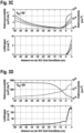
- FIG. 3A shows a current density (top) and a cumulative current density (bottom) as a function of a distance from a SiC/oxide interface in a FinFET for the case of p channel doping and positive interface charge (quadrant I in FIG.
- FIG.3B shows a current density and a cumulative current density as a function of a distance from the SiC/oxide interface in a FinFET for the case of n channel doping and negative interface charge (quadrant III in FIG. 2 ) according to various embodiments
- FIG. 3C shows the FIG. 3A corresponding electron mobility, electron density and conductivity depending on a distance from the SiC/oxide interface
- FIG. 3D shows the FIG.3B corresponding electron mobility, electron density and conductivity depending on a distance from a SiC/oxide interface.
- the channel resistance can be significantly reduced by using a p-doped inversion channel as used in the prior art and in FIG. 2A and FIG. 2B on the right side, and in FIG. 3A and FIG. 3C is shown, to an n-doped accumulation channel, which in FIG. 2A and FIG. 2B on the left side, and in FIG.3B and FIG. 3D is shown.
- FIG. 2 B is a size of an ON resistance, i.e. for a FinFET in the switched-on state, symbolically represented for a parameter field of channel doping and interface charges of the FinFET with 300 nm wide fins and a cell pitch of 800 nm.
- silicon dioxide annealed in a nitrogen oxide atmosphere is used as the gate oxide (as in the state of the art)
- an inversion channel with positive interface charge is formed. This corresponds to circle 36 in the first quadrant (top right) in FIG. 2A and FIG. 2B .
- an accumulation channel with positive interface charge is formed instead (circle 34 in the fourth quadrant top left), the ON resistance is reduced by a factor of about two.
- FinFETs with n-channel doping and positive interface charge have a threshold voltage ⁇ 0V, as in FIG. 2A can be seen in the top left of the fourth quadrant. This is because positive interface charges shift the threshold voltage to smaller values.
- FinFETs that are assigned to the third quadrant, eg with parameters marked by the two stars 38 there, have the advantages described above.
- the interface charges and the channel doping concentration can be determined according to the parameters shown in the third quadrant. Simulation results can be chosen taking into account the desired threshold voltage, e.g. for 3V along the black line.
- a wet-oxidized thermal oxide at 1150°C can be used as the gate dielectric 32, which may be post-treated with NO annealing at 1150°C, or a gate dielectric stack made of SiO 2 and Si 3 N 4 or SiO 2 and Al 2 O 3 .
- the vertical fin field effect transistor 100 can further comprise a p-doped gate shielding region 16, which is arranged under the gate region 24 such that, in vertical projection, the gate shielding region 16 lies at least partially, for example mostly, almost completely or completely, e.g. with at least 50%, at least 60%, at least 70%, at least 80%, at least 90% or at least 95% of its projected area, within an area delimited by the gate dielectric 32.
- the gate shielding region 16 can serve to shield the gate dielectric 32 at the trench bottom from excessively large electric fields.
- the source contact 28 may be electrically conductively connected to the source region 30, and an electrically conductive region 18, 20 may be arranged between the gate region 24 and the p-doped gate shielding region 16, wherein the p-doped Gate shielding region 16 can be electrically conductively connected to the source contact 28 by means of the electrically conductive region 18, 20.
- a second parameter that can influence the channel resistance is the cell spacing (pitch) P, where a smaller pitch P reduces the channel resistance.
- a shielding region is typically realized by means of a deep p-implantation.
- This implantation requires a relatively thick oxide mask (e.g., about 1.5 ⁇ m), which limits the smallest opening that can be achieved - and thus the pitch P.
- a manufacturing method for a FinFET 100 with a reduced cell pitch P is provided.
- a shielding structure is provided by not performing the lithography process limiting the cell pitch between two trenches, but by forming the gate shielding region 16 below the trench.
- the same mask can be used for trench formation and for shield implantation. This means that first the trenches are formed and then (a p-doping) is implanted into the trenches. Thus, the gate shielding region 16 can be formed below the trench.
- the gate shielding region 16 can be formed in a self-aligned manner such that a bottom of the fin 14 and corners of the trench are protected.
- a p-doped layer may also be formed in the trench side walls. In various embodiments, this can be oxidized away in the subsequent fin formation process, so that no p-doping remains in the actual fin 14. Alternatively, a narrow (eg a few 10 nm thick) p-doped zone may remain at the edge of the fin 14.
- An area ratio of p-doped gate shielding region 16 to n-doped spreading region 12, their doping concentrations and geometric arrangement as well as a thickness (depth) of the gate shielding region 16 may be determined by a compromise between shielding (maximum field in the gate dielectric 32, sufficiently small short-circuit current and sufficiently high breakdown voltage) and conductivity at low (ON resistance).
- the spreading region 12 may have several different doping concentrations, for example 2 ⁇ 10 17 cm -3 below and around a lower region of the shielding region 16, and 5 ⁇ 10 17 cm -3 between the shielding regions below the fin 14, which in FIG. 1 as an optional second spreading region 12a is drawn, which extends, for example, to the dot-dash line. This can be helpful in finding a suitable compromise between low on-resistance (high doping between the shielding regions) and high breakdown voltage (small doping below the shielding region).
- the spreading region 12 can extend into the lower region of the fin 14. In particular, into the region next to the electrically conductive region 18, 20, which contacts the gate shielding region 16. Due to a higher doping in this region, this region is conductive even when the gate 24 is switched off and therefore does not have to be switched on by the electric field of the gate 24.
- the p-doped gate shielding region 16 can, in various embodiments, be connected directly to a source potential (the source contact 28) through a contact in the bottom of the trench - the electrically conductive region 18, 20.
- the electrically conductive region 18, 20 can have a contact layer 18 (for example nickel silicide).
- the contact layer 18, or more generally the electrically conductive region 18, 20, can be connected to the source metal by a conductive material (for example a doped or in-situ doped polysilicon).
- the electrically conductive region 18, 20 can be electrically insulated from the gate region 24 by a dielectric layer 22.
- the dielectric layer 22 can be an oxide layer, which can be applied, for example, by means of thermal Oxidizing the electrically conductive region 20, eg in a case where the electrically conductive region 20 comprises polysilicon.
- the connection to the source metal (not shown) can be implemented in various embodiments analogously to a known procedure for the gate connection via a so-called supercell lead-out at the end of the cell field.
- the lead-out of the connection of the gate shielding region 16 to the source contact 28 can be advantageous to keep the lead-out of the connection of the gate shielding region 16 to the source contact 28 as short as possible in order to reduce the resistance.
- This has the advantage that the generation of Joule heat is reduced and the time constant for charging and discharging the shielding region is kept small. Both increase the power efficiency of the component. The latter is particularly advantageous for quickly switching the component.
- the current path from the source contact 28 via the electrically conductive region 20, the shielding region 16 into the drift region 10 represents a diode which must carry current in diode operation. Therefore, a low resistance by a short lead-out of the connection of the shielding region 16 can also be helpful for the functioning of this so-called body diode.
- the electrically conductive region 18, 20 can be formed completely from metal, e.g. from copper or a copper alloy.
- the metal layer 18, 20 and the gate region 24 can be separated from one another by a dielectric 22 deposited (e.g. at low temperatures).
- the metal layer 18, 20 can be deposited, for example, according to or based on a known damascene process.
- the FinFET 100 with the electrically conductive region 18, 20 can have increased robustness against high current densities.
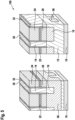
- the vertical Fin-FET 100 which is used in FIG. 5 shown, in various embodiments, further comprise a buried p-doped layer 56.
- the buried p-doped layer 56 may be in contact with the gate shielding region 16.
- the shielding below the trench is composed of the gate shielding region 16 and the buried layer 56.
- a A total depth of the shielding structure 16, 56 in the vertical direction of approximately 1 ⁇ m can be achieved by combining approximately 500 nm thickness of the gate shielding region 16 with approximately 500 nm thickness of the buried layer 56 without having to increase the cell pitch P.
- a vertical FinFET arrangement may further be provided, which comprises a plurality of vertical FinFETs 100 as described above for various embodiments. This is in FIG. 1 , FIG. 4A to 4S and FIG. 5 already indicated by the plurality of Finns 14, Trenches etc.
- the fins 14 may be arranged parallel to one another. They may have an elongated geometry and be arranged parallel to one another along their longitudinal axes.
- the fins 14, trenches and gate shielding regions 16 may extend in a first direction.
- the buried p-doped region 56 may comprise at least one elongated region, e.g. a plurality of mutually parallel elongated regions 56, which extend in a second direction that is different from the first direction.
- the buried regions 56 may be periodically continued in a direction that is different from the direction in which the trenches are periodically continued (see, for example, FIG. 5 ; here the angle between the first direction and the second direction is 90°).
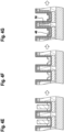
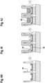
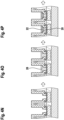
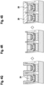
- FIG. 4A to 4S show a schematic illustration of a method for forming a vertical FinFET 100 according to an embodiment. Properties of elements and other features may correspond to what was described above with reference to the vertical FinFET 100.
- FIG.4A First, an n-doped drift region 10, an n-doped spreading region 12 and an n-doped region (from which the fin 14 is later formed) are provided, e.g. by means of epitaxy.
- the Fin 14 extends into the spreading region 12.
- Useful doping concentrations can be, for example, 10 16 cm -3 in the drift region 10, 10 17 cm -3 in the spreading region 12 and 4 ⁇ 10 16 cm -3 in the channel region in the fin 14.
- a planar n-contact source region 30
- a doping concentration of eg 10 19 cm -3 which is either implanted in the channel region or provided as an epitaxial layer.
- Trenches 42 are then produced by means of an etching process using a structured mask 40 (eg oxide hard mask) with widths of approximately 800 nm and a depth of approximately 1.4 ⁇ m, which either extend into the spreading region 12 or stop in front of it. During the process, part of the mask 40 can be removed.
- FIG. 4C The remaining thickness of approximately 800 nm can be used as an implantation mask, thus enabling a self-aligned implantation of the gate shielding region 16 through the trench 42.
- An implantation depth in the trench 42 of approximately 500 nm and a doping of 5 ⁇ 10 19 cm -3 can be achieved with a 0° implantation.
- the mask 40 can then be removed and a contact metal 18 (for example nickel) can be deposited and alloyed over the surface (for example NiSi contact formation using an established RTA process).
- a contact metal 18 for example nickel
- FIG.4D To form the fins 14, protection for the trench bottom can first be provided by producing a structure via a Si 3 N 4 (reference numeral 44) and poly-silicon (reference numeral 46) deposition and poly-silicon 46 etching back ( FIG.4E ), which then allows wet etching of the Si 3 N 4 44, so that only Si 3 N 4 remains at the bottom of the trench ( FIG.4E ).
- the Poly-Si 46 is then also removed ( FIG. 4F ).
- the alloyed contact metal is oxidizable (e.g. NiSi)
- the trench 42 can be enlarged laterally by alternating oxidation and oxide etching, so that in the end only fins 14 remain between the trenches 42.
- the alloyed contact metal can be removed before this step ( FIG. 4G ) can be removed selectively from the Si 3 N 4 and the wafer material (eg SiC) (for example by wet etching). Since the Si 3 N 4 44 at the trench bottom acts as an oxidation barrier because it oxidizes much more slowly than SiC, the contact 18 at the bottom remains protected. The etching of the oxidized areas simultaneously removes the oxidized p-implanted areas on the wafer surface and on the trench side wall, which are undesirable ( FIG. 4G , FIG.4H ). The Si 3 N 4 Protection 44 at the trench bottom is then selectively removed and the gate dielectric 32 is produced ( FIG. 4I ).
- the Si 3 N 4 Protection 44 at the trench bottom is then selectively removed and the gate dielectric 32 is produced ( FIG. 4I ).
- FIG. 4J , FIG.4K : Si 3 N 4 can be deposited in such a way (preferably by means of PECVD or sputter deposition) that overhangs 54 are formed on the fins 14.
- This is a known method with well-known process windows (process gases, process gas flow, process pressure, generator frequency and power) in order to form overhangs 54 close to the surface on free-standing structures with certain aspect ratios.
- the gate oxide 32 in the bottom of the trench 42 can then be opened by means of directed etching (using collimator effects, for example reactive ion etching, RIE, or ion beam etching, IBE) ( FIG. 4L ).
- a poly-Si mask 52 can be used in the trench 42 to change the aspect ratio of the trench 42. This allows the formation of the overhangs 54 to be adjusted and the trench side walls to be better protected.
- the gate oxide 32 which is only open through the access area at the bottom of the trench 42, can be coated with an optional process ( FIG.4M is therefore shown in grey) until most of the bottom, but not the side wall, is exposed.
- the contact 20 to the gate shielding region 16 and the gate 24 together with insulation layers 22, 26 can be introduced into the trench 42 ( FIG. 4O to 4S ). This can be done, for example, by means of double poly-silicon deposition, poly-silicon etching back, poly-silicon re-oxidation, or, for example, by means of a damascene process.
- FIG. 4S front contact 28 and rear contact are formed. For this purpose, ( FIG. 4R ) the oxide above the source region 30 is removed.
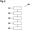
- FIG. 6 is a flow diagram 600 of a method of forming a vertical FinFET according to various embodiments.
- the method may comprise forming a plurality of trenches in an n-doped semiconductor region such that a semiconductor fin with an n-doped channel region is formed between each two of the trenches, which extends between an n-doped drift region and an n-doped source region (610), p-doping semiconductor regions at the respective bottom of the trenches to form p-doped shielding regions (620), forming a dielectric layer on the side walls of the trenches (630), arranging electrically conductive material, which is in electrically conductive contact with the respective shielding region arranged underneath, in the trenches (640), and forming a gate region in each of the trenches above the electrically conductive material and electrically insulated therefrom (650).
Landscapes
- Insulated Gate Type Field-Effect Transistor (AREA)
- Metal-Oxide And Bipolar Metal-Oxide Semiconductor Integrated Circuits (AREA)
Description
- Die Erfindung betrifft einen vertikalen Fin-Feldeffekttransistor (FinFET), eine vertikale Fin-Feldeffekttransistor-Anordnung und ein Verfahren zum Bilden eines vertikalen Fin-Feldeffekttransistors.
- Für die Anwendung von Halbleitern mit breitem Bandabstand (z.B. SiC oder GaN) in der Leistungselektronik kommen typischerweise Leistungs-MOSFETs mit vertikalem Kanalgebiet zum Einsatz. Das Kanalgebiet ist dabei angrenzend an einen Graben (Trench) gebildet, so dass diese Art von MOSFET auch als Trench-MOSFET (TMOSFET) bezeichnet wird. Durch geeignete Wahl von Geometrie und Dotierungskonzentrationen von Epitaxie-, Kanal- und Abschirmbereichen können ein relativ niedriger Einschaltwiderstand und eine relativ hohe Durchbruchspannung erzielt werden.
- Gemäß dem Stand der Technik weist ein Leistungs-Trench-MOSFET eine tiefe p+ Implantation als Abschirmbereich und einen Trench auf, welche periodisch abwechselnd zu einem Zellenfeld aus mehreren einzelnen MOSFETs, die auch als Zellen bezeichnet werden, zusammengesetzt werden. Proportionen von Trench, p+ Abschirmbereich und einem dazwischen gebildeten, mittels eines isolierten Gates schaltbaren Kanalgebiet ergeben sich aus Forderungen, einen möglichst geringen Einschaltwiderstand, eine möglichst niedrige maximale Feldbelastung am Gatedielektrikum, einen möglichst geringen Sättigungsstrom im Kurzschlussfall und eine möglichst hohe Durchbruchspannung zu erzielen. Ein Abstand zwischen gleichartigen Strukturen benachbarter MOSFETs (Pitch) ist dabei begrenzt durch die technischen Möglichkeiten, den Trench zu bilden, die verschiedenen Gebiete zu kontaktieren und die p+ Implantation zu realisieren. Das Dokument
US2014/015036 A1 offenbart einen vertikalen Silizium-Fin-Transistor mit n-dotierten Source/Drain-Bereichen, einem Kanalbereich in der Finne und einem Gate-Bereich, der durch ein Gate-Dielektrikum vom Kanalbereich isoliert ist. Der Transistor umfasst außerdem einen p-dotierten Gate-Abschirmbereich unter dem Gate-Bereich, der über einen leitfähigen Bereich mit der Source elektrisch verbunden ist. - Ein Kanalwiderstand des TMOSFETs ist bestimmt durch die Ladungsträgerverteilung im Kanal und deren Mobilität. Diese beiden Größen werden maßgeblich durch Grenzflächenladungen an einer Grenzfläche zwischen dem Halbleitermaterial im Kanalgebiet und dem Gatedielektrikum bzw. durch Ladungen im Gatedielektrikum und durch die Kanaldotierung bestimmt. Der Zell-Pitch ist maßgeblich bestimmt durch den p+ Abschirmbereich, da zu seiner Herstellung Hochenergie-Implantationen benötigt werden, die wiederum eine ausreichend dicke Maske voraussetzen. Die Dicke dieser Maske limitiert die kleinste Dimension, welche geöffnet werden kann, und darüber den Zell-Pitch.
- In verschiedenen Ausführungsbeispielen wird ein vertikaler Fin-Feldeffekttransistor (vertikaler FinFET, kurz: FinFET; bei einem FinFET besteht die schaltfähige Komponente aus einer schmalen Halbleiter-Finne) mit Trench-Kontakt für eine Abschirmstruktur bereitgestellt. Anschaulich beschrieben ist bei dem vertikalen Fin-Feldeffekttransistor die Abschirmstruktur direkt unterhalb des Grabens angeordnet und mit einem im Graben gebildeten elektrisch leitfähigen Kontakt elektrisch leitfähig verbunden.
- Durch seine Geometrie und durch eine geeignete Wahl von Material und Herstellungsprozess des Gatedielektrikums kann ein besonders geringer Kanalwiderstand ermöglicht werden.
- Die Kontaktierung der Abschirmstruktur durch den Trench kann einen besonders geringen Zellpitch ermöglichen.
- Der FinFET kann beispielsweise als Leistungs-FinFET (Power-FinFET) verwendet werden. Demzufolge kann in verschiedenen Ausführungsbeispielen ein Einschaltwiderstand des Power-FinFETs mit Trench Kontakt deutlich geringer sein als bei einem MOSFET oder MISFET auf Basis von Siliziumcarbid (SiC) oder Galliumnitrid (GaN) gemäß dem Stand der Technik. Hieraus resultieren geringere Verluste im Betrieb des gesamten Bauteils.
- In verschiedenen Ausführungsbeispielen wird ein Leistungs-FinFET mit einem Trenchkontakt zu einer Abschirmstruktur bereitgestellt. Dimensionen, Dotierungen und Grenzflächenladungen an einem Gatedielektrikum (z.B. Gateoxid) können - wie unten näher ausgeführt - so eingerichtet sein, dass ein niedriger Einschaltwiderstand, eine hohe Durchbruchspannung, ein geringer Kurzschlussstrom und eine niedrige maximale Feldbelastung am Gatedielektrikum erzielt werden.
- Ferner wird ein Verfahren bereitgestellt, einen solchen FinFET zu bilden, wobei eine relative Positionierung des Trenches und der Abschirmstruktur selbstjustiert erfolgt. Das bedeutet, dass bei einfacher Herstellung eine hohe relative Positionierungsgenauigkeit erzielbar ist.
- Weiterbildungen der Aspekte sind in den Unteransprüchen und der Beschreibung dargelegt. Ausführungsformen der Erfindung sind in den Figuren dargestellt und in der nachfolgenden Beschreibung näher erläutert. Es zeigen:
- Figur 1
- eine schematische Querschnittsansicht eines vertikalen FinFETs gemäß verschiedenen Ausführungsbeispielen;
- Figur 2A
- eine Veranschaulichung von Schwellspannungen in FinFETs in Abhängigkeit von einer Kanaldotierungskonzentration und einer Grenzflächenladung;
- Figur 2B
- eine Veranschaulichung von Einschaltwiderständen in FinFETs in Abhängigkeit von einer Kanaldotierungskonzentration und einer Grenzflächenladung;
- Figur 3A
- eine Stromdichte und eine kumulierte Stromdichte in Abhängigkeit von einem Abstand von einer SiC/Oxid Grenzfläche in einem FinFET;
- Figur 3B
- eine Stromdichte und eine kumulierte Stromdichte in Abhängigkeit von einem Abstand von einer SiC/Oxid Grenzfläche in einem FinFET gemäß verschiedenen Ausführungsbeispielen;
- Figur 3C
- eine Elektronenmobilität, eine Elektronendichte und eine Leitfähigkeit in Abhängigkeit von einem Abstand von einer SiC/Oxid Grenzfläche in einem FinFET;
- Figur 3D
- eine Elektronenmobilität, eine Elektronendichte und eine Leitfähigkeit in Abhängigkeit von einem Abstand von einer SiC/Oxid Grenzfläche in einem FinFET gemäß verschiedenen Ausführungsbeispielen;
- Figuren 4A bis 4S
- eine schematische Veranschaulichung eines Verfahrens zum Bilden eines vertikalen FinFETs gemäß verschiedenen Ausführungsbeispielen;
- Figur 5
- eine schematische perspektivische Vorder- und Rückseitenansicht eines FinFETs gemäß verschiedenen Ausführungsbeispielen; und
- Figur 6
- ein Ablaufdiagramm eines Verfahrens zum Bilden eines vertikalen FinFETs gemäß verschiedenen Ausführungsbeispielen.
- In
FIG. 1 ist eine schematische Querschnittsansicht eines vertikalen FinFETs 100 gemäß verschiedenen Ausführungsbeispielen dargestellt. - Der vertikale Fin-Feldeffekttransistor 100 kann eine n-dotierte Halbleiter-Finne 14 (kurz: Finne) aufweisen, welche sich vertikal zwischen einem n-dotierten Sourcebereich 30 (oberhalb oder im oberen Ende der Finne 14) und einem n-dotierten Driftbereich 10, 12 (unterhalb der Finne 14) des FinFETs erstrecken kann. Der Driftbereich 10, 12 kann ein n-dotiertes Driftgebiet 10 und ein n-dotiertes Ausbreitungsgebiet (Spreadinggebiet) 12 aufweisen. Eine Dotierungskonzentration kann in verschiedenen Ausführungsbeispielen im Spreadinggebiet 12 höher sein als im darunter angeordneten Driftgebiet 10, und höher sein als im darüber angeordneten n-Kanalgebiet in der Halbleiter-Finne 14. Bei einem Ausführungsbeispiel können die Dotierungen zum Beispiel 1016 cm-3 im Driftgebiet 10, 1017 cm-3 im Spreadinggebiet 12 und 4.1016 cm-3 im Kanalgebiet in der Finne 14 sein. Das n-dotierte Halbleitermaterial des Driftbereichs 10, 12 und der Finne 14 kann als epitaktisch aufgewachsenes Material bereitgestellt sein bzw. werden, z.B. aufgewachsen auf einem Substrat, ggf. mit zwischen dem Driftbereich 10, 12 und dem Substrat angeordneter Pufferschicht. Auf einer Rückseite des Substrats kann ein Drainkontakt angeordnet sein. Substrat, Drainkontakt und ggf. Pufferschicht können auf bekannte oder im Wesentlichen bekannte Weise hergestellt sein.
- Der vertikale Fin-Feldeffekttransistor 100 kann ferner mindestens einen dem Kanalbereich horizontal benachbarten Gatebereich 24 aufweisen. Im Ausführungsbeispiel aus
FIG. 1 sind horizontal benachbart zur Finne 14 zwei Gatebereiche 24 gebildet, welche von der Finne 14 durch ein Gatedielektrium 32 und von einem darüber angeordneten Sourcekontakt 28 mittels eines weiteren Dielektrikums 26 elektrisch isoliert sein können. Der Gatebereich 24 kann ein leitfähiges Material aufweisen, beispielsweise Poly-Silizium. In verschiedenen Ausführungsbeispielen kann an dessen Oberfläche mittels Re-Oxidation das weitere Dielektrikum 26 als Isolierung zum Sourcekontakt 28 gebildet werden. - An einer Grenzfläche zwischen dem Gatedielektrikum 32 und dem Kanalbereich 14 bzw. im Gatedielektrikum 32 selbst können negative Grenzflächenladungen vorliegen.
- Eigenschaften eines FinFETS mit einer solchen Gestaltung 100 sind in
FIG. 2A und 2B und inFIG. 3A bis 3D dargestellt. - In
FIG. 2A sind in einem Schaubild 200 Schwellspannungen Vt in FinFETs veranschaulicht in Abhängigkeit von einer Kanaldotierungskonzentration und einer Grenzflächenladung,FIG. 2B zeigt in einem Schaubild 202 eine Veranschaulichung von Einschaltwiderständen in FinFETs in Abhängigkeit von einer Kanaldotierungskonzentration und einer Grenzflächenladung,FIG. 3A zeigt eine Stromdichte (oben) und eine kumulierte Stromdichte (unten) in Abhängigkeit von einem Abstand von einer SiC/Oxid Grenzfläche in einem FinFET für den Fall von p Kanaldotierung und positiver Grenzflächenladung (Quadrant I inFIG. 2 ) wie der Kanal gemäß dem Stand der Technik für einen TMOSFET verwendet wird,FIG. 3B zeigt eine Stromdichte und eine kumulierte Stromdichte in Abhängigkeit von einem Abstand von der SiC/Oxid Grenzfläche in einem FinFET für den Fall von n Kanaldotierung und negativer Grenzflächenladung (Quadrant III inFIG. 2 ) gemäß verschiedenen Ausführungsbeispielen,FIG. 3C zeigt die zuFIG. 3A entsprechende Elektronenmobilität, Elektronendichte und Leitfähigkeit in Abhängigkeit von einem Abstand von der SiC/Oxid Grenzfläche, undFIG. 3D zeigt die zuFIG. 3B entsprechende Elektronenmobilität, Elektronendichte und Leitfähigkeit in Abhängigkeit von einem Abstand von einer SiC/Oxid Grenzfläche. - Der Kanalwiderstand kann signifikant verringert werden, wenn von einem p-dotierten Inversionskanal, wie er gemäß dem Stand der Technik verwendet wird und in
FIG. 2A und FIG. 2B jeweils auf der rechten Seite, und inFIG. 3A undFIG. 3C dargestellt ist, zu einem n-dotiertem Akkumulationskanal übergegangen wird, welcher inFIG. 2A und FIG. 2B jeweils auf der linken Seite, und inFIG. 3B undFIG. 3D dargestellt ist. - In
FIG. 2B ist eine Größe eines ON-Widerstands, also für einen FinFET im eingeschalteten Zustand, symbolisch dargestellt für ein Parameterfeld von Kanaldotierungen und Grenzflächenladungen des FinFETs mit 300 nm breiten Finnen und einem Zell-Pitch von 800 nm. Wird als Gateoxid ein in Stickoxidatmosphäre getempertes Siliziumdioxid verwendet (wie beim Stand der Technik), wird ein Inversionskanal mit positiver Grenzflächenladung gebildet. Das entspricht dem Kreis 36 im ersten Quadranten (rechts oben) inFIG. 2A und FIG. 2B . Wird stattdessen ein Akkumulationskanal mit positiver Grenzflächenladung gebildet (Kreis 34 im vierten Quadranten links oben), reduziert sich der ON-Widerstand um ca. einen Faktor zwei. Allerdings haben FinFETs mit n-Kanal Dotierung und positiver Grenzflächenladung eine Schwellspannung < 0V, wie inFIG. 2A links oben im vierten Quadranten zu sehen ist. Dies hängt damit zusammen, dass positive Grenzflächenladungen die Schwellspannung zu kleineren Werten hin verschiebt. Durch die Wahl eines Gatedielektrikums oder Gatedielektrikum-Stapels oder einer geeigneten Vor- oder Nach-Behandlungsmethode kann eine Grenzfläche Kanal-Halbleitermaterial/Gatedielektrikum mit negativen Grenzflächenladungen erzeugt werden oder negative Ladungen ins Gatedielektrikum eingebaut werden. - Das kann dazu führen, dass Kombinationen aus Grenzflächenladungen und Kanaldotierungen ermittelbar sind, die sowohl eine geeignete positive Schwellspannung (z.B. 3V, schwarze Linie in
FIG. 2B ) als auch einen geringeren ON-Widerstand liefern als ein FinFET mit einer SiC/Gatedielektrikum Grenzfläche gemäß dem Stand der Technik. Diese Kombinationen sind beispielsweise im zweiten und dritten Quadranten sowohl für Inversion (zweiter Quadrant) als auch für Akkumulation (dritter Quadrant) auffindbar, z.B. entlang der schwarzen Linie im zweiten bzw. dritten Quadranten. - Insbesondere FinFETs, die dem dritten Quadranten zuzuordnen sind, z.B. mit Parametern, die durch die beiden Sterne 38 dort markiert sind, weisen die oben beschriebenen Vorteile auf. Beim FinFET 100 gemäß verschiedenen Ausführungsbeispielen können die Grenzflächenladungen und die Kanaldotierungskonzentration gemäß den im dritten Quadranten dargestellten Simulationsergebnissen unter Berücksichtigung der gewünschten Schwellspannung gewählt werden, z.B. für 3V entlang der schwarzen Linie.
- Als Gatedielektrikum 32 kann in verschiedenen Ausführungsbeispielen ein nassoxidiertes thermisches Oxid bei 1150°C verwendet werden, das ggf. mit einem NO-Tempern bei 1150°C nachbehandelt wird, oder ein Gatedielektrikums-Stapel aus SiO2 und Si3N4 oder SiO2 und Al2O3.
- Wie oben erwähnt ist ein Grund für die Verringerung des ON-Widerstands die Ladungsträgerverteilung im Kanal und deren Mobilität. Dies wird anschaulich anhand eines Vergleichs von Stromdichten für Inversionskanäle (
FIG. 3A ,FIG. 3C ) und Akkumulationskanäle (FIG. 3B ,FIG. 3D ) mit jeweils 3V Schwellspannung im Querschnitt der Finne 14. - Während die Stromdichte im Inversionskanal (
FIG. 3A ,FIG. 3C ) ausschließlich in den ersten 5-10 nm zur SiC/Gate-Oxid Grenzfläche getragen wird, also nur dort signifikante Werte annimmt, geht die Stromverteilung im Akkumulationskanal (FIG. 3B ,3D ) viel tiefer in die Finne 14 hinein. Dort ist, wie inFIG. 3C und 3D unten zu sehen ist, die Leitfähigkeit deutlich höher. Somit ergibt sich eine höhere Leitfähigkeit im Kanal, der sich nahezu über die gesamte Finnenbreite wC (sieheFIG. 1 ) erstreckt. - Der vertikale Fin-Feldeffekttransistor 100 kann ferner einen p-dotierten Gate-Abschirmbereich 16 aufweisen, welcher so unter dem Gatebereich 24 angeordnet ist, dass bei vertikaler Projektion der Gate-Abschirmbereich 16 zumindest teilweise, beispielsweise größtenteils, fast vollständig oder vollständig, z.B. mit mindestens 50%, mindestens 60%, mindestens 70%, mindestens 80%, mindestens 90% oder mindestens 95% seiner projizierten Fläche, innerhalb einer vom Gatedielektrikum 32 begrenzten Fläche liegt. Der Gate-Abschirmbereich 16 kann dazu dienen, das Gatedielektrikum 32 am Trenchboden vor zu großen elektrischen Feldern abzuschirmen.
- Der Sourcekontakt 28 kann elektrisch leitend mit dem Sourcebereich 30 verbunden sein, und ein elektrisch leitfähiger Bereich 18, 20 kann zwischen dem Gatebereich 24 und dem p-dotierten Gate-Abschirmbereich 16 angeordnet sein, wobei der p-dotierte Gate-Abschirmbereich 16 mittels des elektrisch leitfähigen Bereichs 18, 20 mit dem Sourcekontakt 28 elektrisch leitfähig verbunden sein kann.
- Ein zweiter Parameter, welcher den Kanalwiderstand beeinflussen kann, ist der Zellabstand (Pitch) P, wobei ein kleinerer Pitch P den Kanalwiderstand verkleinert.
- Gemäß dem Stand der Technik wird ein Abschirmbereich typischerweise mittels einer tiefen p-Implantation verwirklicht. Für diese Implantation wird eine relativ (z.B. ca. 1,5 µm) dicke Oxidmaske benötigt, welche die kleinste Öffnung, die erreicht werden kann - und damit den Pitch P - begrenzt.
- In verschiedenen Ausführungsbeispielen wird ein Herstellungsverfahren für einen FinFET 100 mit verkleinertem Zell-Pitch P bereitgestellt. Bei dem Verfahren wird eine Abschirmstruktur bereitgestellt, indem der den Zell-Pitch begrenzende Lithographievorgang nicht zwischen zwei Trenches ausgeführt wird, sondern der Gate-Abschirmbereich 16 unterhalb des Trenches ausgebildet wird.
- In verschiedenen Ausführungsbeispielen kann dieselbe Maske für die Trenchbildung und für die Abschirmungsimplantation genutzt werden. Das heißt, zunächst werden die Trenches gebildet, und anschließend in die Trenches (eine p-Dotierung) hineinimplantiert. Somit kann der Gate-Abschirmbereich 16 unterhalb des Trenches gebildet werden.
- Das bedeutet, dass mittels eines einfachen Verfahrens gemäß verschiedenen Ausführungsbeispielen der Gate-Abschirmbereich 16 selbstjustiert so gebildet werden kann, dass ein Boden der Finne 14 und Ecken des Trenches geschützt sind.
- Beim Dotierprozess zum Bilden des Gate-Abschirmbereichs 16 kann es dazu kommen, dass auch in den Trench-Seitenwänden eine p-dotierte Schicht gebildet wird. Diese kann in verschiedenen Ausführungsbeispielen im anschließenden Finnenbildungsprozess wegoxidiert werden, so dass in der eigentlichen Finne 14 keine p-Dotierung übrigbleibt. Alternativ kann am Rand der Finne 14 eine schmale (z.B. wenige 10 nm dicke) p-dotierte Zone übrigbleiben.
- Ein Flächenverhältnis von p-dotiertem Gate-Abschirmbereich 16 zu n-dotiertem Spreadinggebiet 12, ihre Dotierungskonzentrationen und geometrische Anordnung sowie eine Dicke (Tiefe) des Gate-Abschirmbereichs 16 können bestimmt sein durch einen Kompromiss aus Abschirmung (maximales Feld im Gatedielektrikum 32, ausreichend kleiner Kurzschlussstrom und ausreichend hohe Durchbruchspannung) und Leitfähigkeit bei niedrigen (ON-Widerstand). Insbesondere kann in einer Ausführungsform das Spreadinggebiet 12 mehrere unterschiedliche Dotierungskonzentrationen aufweisen, zum Beispiel 2·1017cm-3 unterhalb und um einen unteren Bereich des Abschirmbereichs 16 herum, und 5·1017cm-3 zwischen den Abschirmbereichen unterhalb der Finne 14, was in
FIG. 1 als ein optionales zweites Spreadinggebiet 12a eingezeichnet ist, welches beispielsweise bis zur strichpunktierten Linie reicht. Dies kann hilfreich sein, um einen geeigneten Kompromiss zwischen geringem Einschaltwiderstand (hohe Dotierung zwischen den Abschirmbereichen) und hoher Durchbruchspannung (kleine Dotierung unterhalb des Abschirmbereichs) zu finden. - Außerdem kann das Spreadinggebiet 12 in einer Ausführungsform in den unteren Bereich der Finne 14 hineinragen. Insbesondere in den Bereich neben dem elektrisch leitfähigen Bereich 18, 20, der den Gate-Abschirmbereich 16 kontaktiert. Durch eine höhere Dotierung in diesem Bereich ist dieses Gebiet auch bei ausgeschaltetem Gate 24 leitfähig und muss somit vom elektrischen Feld des Gates 24 nicht aufgeschaltet werden.
- Der p-dotierte Gate-Abschirmbereich 16 kann in verschiedenen Ausführungsbeispielen direkt durch einen Kontakt im Boden des Trenches - den elektrisch leitfähigen Bereich 18, 20 - an ein Sourcepotential (den Sourcekontakt 28) angeschlossen werden. Der elektrisch leitfähige Bereich 18, 20 kann in verschiedenen Ausführungsbeispielen eine Kontaktschicht 18 (zum Beispiel Nickel-Silizid) aufweisen. Die Kontaktschicht 18, bzw. allgemeiner der elektrisch leitfähige Bereich 18, 20, kann durch ein leitfähiges Material (zum Beispiel ein dotiertes- bzw. in-situ dotiertes Poly-Silizium) an das Source-Metall angeschlossen werden. Vom Gatebereich 24 kann der elektrisch leitfähige Bereich 18, 20 in verschiedenen Ausführungsbeispielen durch eine dielektrische Schicht 22 elektrisch isoliert sein. Die dielektrische Schicht 22 kann in verschiedenen Ausführungsbeispielen eine Oxidschicht sein, die beispielsweise mittels thermischen Oxidierens des elektrisch leitfähigen Bereichs 20 gebildet sein bzw. werden kann, z.B. in einem Fall, dass der elektrisch leitfähige Bereich 20 Polysilizium aufweist. Der (nicht dargestellte) Anschluss an das Source-Metall kann in verschiedenen Ausführungsbeispielen analog zu einem bekannten Vorgehen beim Gate-Anschluss über eine so genannte Superzellen-Hinausführung am Ende des Zellenfeldes verwirklicht werden.
- Es kann in verschiedenen Ausführungsbeispielen vorteilhaft sein, eine Herausführung des Anschlusses des Gate-Abschirmbereichs 16 zum Source-Kontakt 28 möglichst kurz zu halten, um den Widerstand zu verkleinern. Dies hat den Vorteil, dass die Entstehung von Joulescher Wärme verringert wird und die Zeitkonstante zum Be- und Entladen des Abschirmungsgebiets klein gehalten wird. Beides erhöht die Leistungseffizienz des Bauteils. Letzteres ist insbesondere zum schnellen Schalten des Bauteils vorteilhaft. Des Weiteren stellt der Strompfad vom Source-Kontakt 28 über den elektrisch leitfähigen Bereich 20, den Abschirmbereich 16 in den Driftbereich 10 eine Diode dar, welche im Diodenbetrieb Strom tragen muss. Daher kann auch für das Funktionieren dieser sogenannten Bodydiode ein geringer Widerstand durch eine kurze Herausführung des Anschlusses des Abschirmbereichs 16 hilfreich sein. In verschiedenen Ausführungsbeispielen kann der elektrisch leitfähige Bereich 18, 20 vollständig aus Metall, z.B. aus Kupfer oder einer Kupferlegierung, gebildet sein bzw. werden. In dem Fall können die Metallschicht 18, 20 und der Gatebereich 24 durch ein (z.B. bei niedrigen Temperaturen) deponiertes Dielektrikum 22 voneinander getrennt werden. Die Metallschicht 18, 20 kann beispielsweise gemäß einem oder in Anlehnung an einen bekannten Damascene-Prozess abgelagert werden bzw. sein. Der FinFET 100 mit dem elektrisch leitfähigen Bereich 18, 20 kann eine erhöhte Robustheit gegenüber hohen Stromdichten aufweisen.
- Um eine noch bessere Abschirmung und insbesondere einen höheren Widerstand bei hohen Drain-Spannungen und damit einen geringeren Kurzschlussstrom zu erzielen, kann der vertikale Fin-FET 100, der in
FIG. 5 dargestellt ist, in verschiedenen Ausführungsbeispielen ferner eine vergrabene p-dotierte Schicht 56 aufweisen. Die vergrabene p-dotierte Schicht 56 kann in Kontakt sein mit dem Gate-Abschirmgebiet 16. Damit wird die Abschirmung unterhalb des Trenches aus dem Gate-Abschirmgebiet 16 sowie der vergrabenen Schicht 56 zusammensetzt. Somit kann beispielsweise eine Gesamttiefe der Abschirmstruktur 16, 56 in vertikaler Richtung von ca. 1 µm erreicht werden, indem etwa 500 nm Dicke des Gate-Abschirmgebietes 16 mit etwa 500 nm Dicke der vergrabenen Schicht 56 miteinander kombiniert werden, ohne dass der Zell-Pitch P vergrößert werden muss. - In verschiedenen Ausführungsbeispielen kann ferner eine vertikale FinFET-Anordnung bereitgestellt werden, die eine Mehrzahl von vertikalen FinFETs 100 wie oben für verschiedene Ausführungsbeispiele beschrieben aufweist. Das ist in
FIG. 1 ,FIG. 4A bis 4S undFIG. 5 bereits angedeutet durch die Mehrzahl von Finnen 14, Trenches usw. - Die Finnen 14 (und dementsprechend auch die Trenches und die darunter gebildeten Gate-Abschirmbereiche 16) können parallel zueinander angeordnet sein. Sie können eine langgestreckte Geometrie aufweisen und entlang ihrer Längsachsen parallel zueinander angeordnet sein. Die Finnen 14, Trenches und Gate-Abschirmbereiche 16 können sich in einer ersten Richtung erstrecken.
- Um Justierungs- (Alignment)-Probleme zwischen der vergrabenen Schicht 56 und den Strukturen der FinFETs 100 zu vermeiden, kann der vergrabene p-dotierte Bereich 56 mindestens einen langgestreckten Bereich, z.B. eine Mehrzahl zueinander paralleler langgestreckter Bereiche 56 aufweisen, welche/r sich in einer zweiten Richtung erstreckt/erstrecken, die von der ersten Richtung verschieden ist. Anders ausgedrückt können die vergrabenen Bereiche 56 in einer Richtung periodisch fortgesetzt sein, die unterschiedlich ist zu der Richtung, in der die Trenches periodisch fortgesetzt sind (siehe zum Beispiel
FIG. 5 ; hier beträgt der Winkel zwischen der ersten Richtung und der zweiten Richtung 90°). -
FIG. 4A bis 4S zeigen eine schematische Veranschaulichung eines Verfahrens zum Bilden eines vertikalen FinFETs 100 gemäß einem Ausführungsbeispiel. Eigenschaften von Elementen und sonstigen Merkmalen können dabei dem entsprechen, was oben mit Bezug auf den vertikalen FinFET 100 beschrieben wurde. -
FIG. 4A : Zunächst werden ein n-dotiertes Driftgebiet 10, ein n-dotiertes Spreadinggebiet 12 und ein n-dotiertes Gebiet (aus welchem später die Finne 14 gebildet wird) bereitgestellt, z.B. mittels Epitaxie. In verschiedenen Ausführungsbeispielen kann die Finne 14 in das Spreadinggebiet 12 hineinragen. Sinnvolle Dotierungskonzentrationen können zum Beispiel 1016 cm-3 im Driftgebiet 10, 1017 cm-3 im Spreadinggebiet 12 und 4·1016 cm-3 im Kanalgebiet in der Finne 14 sein. Danach folgt ein flächiger n-Kontakt (Sourcebereich 30), z.B. mit einer Dotierungskonzentration von z.B. 1019cm-3, der entweder in das Kanalgebiet implantiert wird oder auch als epitaktische Schicht bereitgestellt wird.FIG. 4B : Danach werden Trenches 42 mittels eines Ätzprozesses unter Verwendung einer strukturierten Maske 40 (z.B. Oxid-Hartmaske) hergestellt mit Breiten von ca. 800 nm und einer Tiefe von ca. 1,4 µm, welche entweder bis in das Spreadinggebiet 12 hineinreichen oder davor stoppen. Während des Prozesses kann ein Teil der Maske 40 abgetragen werden.FIG. 4C : Die verbleibende restliche Dicke von ca. 800 nm kann als Implantationsmaske verwendet werden und so eine selbstjustierte Implantation des Gate-Abschirmbereichs 16 durch den Trench 42 ermöglicht werden. Eine Implantationstiefe im Trench 42 von ca. 500 nm und eine Dotierung von 5·1019 cm-3 können mit einer 0° Implantation erreicht werden. Anschließend kann die Maske 40 entfernt werden und flächig ein Kontaktmetall 18 (zum Beispiel Nickel) deponiert und einlegiert werden (z.B. NiSi-Kontaktbildung mittels eines etablierten RTA-Prozesses). -
FIG. 4D : Zum Bilden der Finnen 14 kann zunächst ein Schutz für den Trenchboden bereitgestellt werden, indem über eine Si3N4 (Bezugszeichen 44) und Poly-Silizium (Bezugszeichen 46) Deposition und Poly-Silizium 46 Rückätzung eine Struktur hergestellt wird (FIG. 4E ), die anschließend ein Nassätzen des Si3N4 44 erlaubt, so dass nur am Boden des Trenches Si3N4 übrigbleibt (FIG. 4E ). Das Poly-Si 46 wird danach ebenfalls entfernt (FIG. 4F ). Nun kann, sofern das einlegierte Kontaktmetall oxidierbar ist (z.B. NiSi) durch abwechselnde Oxidation und Oxidätzung der Trench 42 lateral vergrößert werden, so dass am Ende nur noch Finnen 14 zwischen den Trenches 42 übrigbleiben. Bei nicht oxidierbarem Kontaktmetall kann das einlegierte Kontaktmetall vor diesem Schritt (FIG. 4G ) selektiv zum Si3N4 und zum Wafermaterial (z.B. SiC) entfernt werden (zum Beispiel durch Nassätzung). Da das Si3N4 44 am Trenchboden als Oxidationsbarriere fungiert, weil es deutlich langsamer oxidiert als SiC, bleibt der Kontakt 18 am Boden geschützt. Die Ätzung der oxidierten Bereiche entfernt zugleich auch die oxidierten p-implantierten Bereiche auf der Waferoberfläche und an der Trenchseitenwand, welche unerwünscht sind (FIG. 4G ,FIG. 4H ). Der Si3N4 Schutz 44 am Trenchboden wird anschließend selektiv entfernt und das Gatedielektrikum 32 hergestellt (FIG. 4I ). - Die Öffnung zum Anschluss der p-Abschirmung 16 benötigt wiederum einige Prozessschritte.
FIG. 4J ,FIG. 4K : Si3N4 kann derart abgeschieden werden (vorzugsweise mittels PECVD oder Sputterdeposition), dass sich an den Finnen 14 Überhänge 54 ergeben. Dies ist eine bekannte Methode mit wohlbekannten Prozessfenstern (Prozessgase, Prozessgasführung, Prozessdruck, Generatorfrequenz und Leistung), um an freistehenden Strukturen bestimmter Aspektverhältnisse oberflächennahe Überhänge 54 auszubilden. Mittels gerichteter Ätzung (unter Ausnutzung von Kollimatoreffekten, zum Beispiel Reaktivem Ionenätzen, RIE, oder Ionenstrahlätzen, IBE) kann dann das Gateoxid 32 im Boden des Trenches 42 geöffnet werden (FIG. 4L ). Alternativ kann mit einer Poly-Si-Maske 52 im Trench 42 gearbeitet werden, um das Aspektverhältnis des Trenches 42 zu ändern. Damit können das Ausbilden der Überhänge 54 angepasst und die Trench-Seitenwände besser geschützt werden. Um die Kontaktfläche am Boden des Trenches zu erweitern, kann das Gateoxid 32, welches nur durch den Zugangsbereich am Boden des Trenches 42 geöffnet ist, bei einem optionalen Prozess (FIG. 4M ist deshalb ausgegraut dargestellt) auf Zeit nass geätzt werden, bis der Großteil des Bodens, aber noch nicht die Seitenwand, frei gelegt ist. - Nachdem das Si3N4 54 und ggf. die Poly-Si Maske 52 entfernt sind, können der Kontakt 20 zum Gate-Abschirmbereich 16 und das Gate 24 mitsamt Isolationsschichten 22, 26 in den Trench 42 eingebracht werden (
FIG. 4O bis 4S ). Dies kann beispielsweise mittels zweifacher Poly-Silizium Deposition, Poly-Silizium Rückätzung, Poly-Silizium Re-Oxidation durchgeführt werden, oder beispielsweise mittels eines Damascene-Prozesses. Zuletzt (FIG. 4S ) werden Vorderseitenkontakt 28 und Rückseitenkontakt gebildet. Dazu wurde zuvor (FIG. 4R ) das Oxid oberhalb des Sourcebereichs 30 entfernt. -
FIG. 6 ist ein Ablaufdiagramm 600 eines Verfahrens zum Bilden eines vertikalen FinFETs gemäß verschiedenen Ausführungsbeispielen. - Das Verfahren kann ein Bilden mehrerer Gräben in einem n-dotierten Halbleiterbereich, derart, dass jeweils zwischen zwei der Gräben eine Halbleiter-Finne mit einem n-dotierten Kanalbereich gebildet wird, welche sich zwischen einem n-dotierten Driftbereich und einem n-dotierten Sourcebereich erstreckt (610), ein p-Dotieren von Halbleiterbereichen am jeweiligen Boden der Gräben zum Bilden p-dotierter Abschirmbereiche (620), ein Bilden einer dielektrischen Schicht auf den Seitenwänden der Gräben (630), ein Anordnen von elektrisch leitfähigem Material, welches in elektrisch leitfähigem Kontakt mit dem jeweiligen darunter angeordneten Abschirmbereich ist, in den Gräben (640) und ein Bilden jeweils eines Gatebereichs in den Gräben über dem elektrisch leitfähigen Material und von diesem elektrisch isoliert aufweisen (650).
Claims (11)
- Vertikaler Fin-Feldeffekttransistor (100), aufweisend:• eine Halbleiter-Finne (14);• einen n-dotierten Sourcebereich (30);• einen n-dotierten Driftbereich (10);• einen vertikal zwischen dem Sourcebereich (30) und dem Driftbereich (10) angeordneten n-dotierten Kanalbereich in der Halbleiter-Finne (14);• mindestens einen dem Kanalbereich horizontal benachbarten Gatebereich (24);• ein Gatedielektrium (32), welches den Gatebereich (24) vom Kanalbereich elektrisch isoliert, wobei eine Grenzflächenschicht zwischen dem Gatedielektrikum (32) und dem Kanalbereich und/oder das Gatedielektrikum (32) negative Grenzflächenladungen aufweist;• einen p-dotierten Gate-Abschirmbereich (16), welcher so unter dem Gatebereich (24) angeordnet ist, dass bei vertikaler Projektion der Gate-Abschirmbereich (16) zumindest teilweise innerhalb einer vom Gatedielektrikum (32) begrenzten Fläche liegt.• einen Sourcekontakt (28), welcher elektrisch leitend mit dem Sourcebereich (30) verbunden ist; und• einen elektrisch leitfähigen Bereich (18, 20) zwischen dem Gatebereich (24) und dem p-dotierten Gate-Abschirmbereich (16);• wobei der p-dotierte Gate-Abschirmbereich (16) mittels des elektrisch leitfähigen Bereichs (18, 20) mit dem Sourcekontakt (28) elektrisch leitfähig verbunden ist.
- Vertikaler Fin-Feldeffekttransistor (100) gemäß Anspruch 1,
wobei der elektrisch leitfähige Bereich (18, 20) Polysilizium aufweist, und/oder eine leitfähige Schicht (18) aufweist, die Metall oder ein Nickel-Silizid aufweist. - Vertikaler Fin-Feldeffekttransistor (100) gemäß einem der Ansprüche 1 oder 2, wobei die Halbleiter-Finne (14) Siliziumcarbid und/oder Galliumnitrid aufweist.
- Vertikaler Fin-Feldeffekttransistor (100) gemäß einem der Ansprüche 1 bis 3, wobei der Kanalbereich eine Breite aufweist in einem Bereich von 50 nm bis 400 nm, und wobei eine Dotierungskonzentration im Kanalbereich in einem Bereich von 1015cm-3 bis 1017cm-3 liegt.
- Vertikaler Fin-Feldeffekttransistor (100) gemäß einem der Ansprüche 1 bis 4, ferner aufweisend:
mindestens ein Spreadinggebiet, (12, 12a) welches höher n-dotiert ist als der Driftbereich (10). - Vertikaler Fin-Feldeffekttransistor (100) gemäß Anspruch 5,wobei das mindestens eine Spreadinggebiet (12, 12a) ein erstes Spreadinggebiet (12) aufweist, welches unterhalb und um einen unteren Bereich des Gate-Abschirmbereichs (16) herum angeordnet ist, und ein zweites Spreadinggebiet (12a) lateral benachbart zum Gate-Abschirmbereich (16) über dem ersten Spreadinggebiet (12), wobei das zweite Spreadinggebiet (12a) höher dotiert ist als das erste Spreadinggebiet (12); undwobei optional das zweite Spreadinggebiet (12a) in einen unteren Bereich der Finne (14) hineinragt, insbesondere in einen Bereich benachbart zu dem elektrisch leitfähigen Bereich (18, 20).
- Fin-Feldeffekttransistor-Anordnung, aufweisend:• eine Mehrzahl von vertikalen Fin-Feldeffekttransistoren (100) gemäß einem der Ansprüche 1 bis 4, welche parallel zueinander angeordnet sind, derart, dass ihre jeweiligen p-dotierten Gate-Abschirmbereiche (16) sich in einer ersten Richtung erstrecken.
- Fin-Feldeffekttransistor-Anordnung gemäß Anspruch 7, ferner aufweisend:
eine Mehrzahl von vergrabenen p-dotierten Bereichen (56), welche unter den p-dotierten Gate-Abschirmbereichen (16) und in Kontakt mit den p-dotierten Gate-Abschirmbereichen (16) parallel zueinander angeordnet sind und sich in einer zweiten Richtung erstrecken, wobei die zweite Richtung optional verschieden ist von der ersten Richtung. - Verfahren zum Bilden eines vertikalen Fin-Feldeffekttransistors, aufweisend:• Bilden mehrerer Gräben in einem n-dotierten Halbleiterbereich, derart, dass jeweils zwischen zwei der Gräben eine Halbleiter-Finne mit einem n-dotierten Kanalbereich gebildet wird, welche sich zwischen einem n-dotierten Driftbereich und einem n-dotierten Sourcebereich erstreckt (610);• p-Dotieren von Halbleiterbereichen am jeweiligen Boden der Gräben zum Bilden p-dotierter Abschirmbereiche (620);• Bilden einer dielektrischen Schicht auf den Seitenwänden der Gräben (630);• Anordnen von elektrisch leitfähigem Material, welches in elektrisch leitfähigem Kontakt mit dem jeweiligen darunter angeordneten Abschirmbereich ist, in den Gräben (640);• Bilden jeweils eines Gatebereichs (24) in den Gräben über dem elektrisch leitfähigen Material und von diesem elektrisch isoliert (650).
- Verfahren gemäß Anspruch 9,
wobei das Anordnen von elektrisch leitfähigem Material ein Bilden einer leitfähigen Schicht aufweist, die Metall oder ein Nickel-Silizid aufweist, und/oder ein Bilden von Polysilizium-Bereichen in den Gräben. - Verfahren gemäß Anspruch 9 oder 10, wobei die Gräben sich parallel zueinander in einer ersten Richtung erstrecken, das Verfahren ferner aufweisend:• Bilden eines unteren n-dotierten Halbleiterbereichs;• p-Dotieren mindestens eines langgestreckten Bereichs in dem unteren n-dotierten Halbleiterbereich, welcher sich in einer zweiten Richtung erstreckt;• Bilden des n-dotierten Halbleiterbereichs auf dem unteren n-dotierten Halbleiterbereich und dem langgestreckten Bereich;• wobei die erste Richtung verschieden ist von der zweiten Richtung; und• wobei das p-Dotieren der Halbleiterbereiche am jeweiligen Boden der Gräben derart erfolgt, dass die p-dotierten Abschirmbereiche den langgestreckten Bereich kontaktieren.
Applications Claiming Priority (2)
| Application Number | Priority Date | Filing Date | Title |
|---|---|---|---|
| DE102020202038.8A DE102020202038A1 (de) | 2020-02-18 | 2020-02-18 | Vertikaler Fin-Feldeffekttransistor, vertikaler Fin-Feldeffekttransistor-Anordnung und Verfahren zum Bilden eines vertikalen Fin-Feldeffekttransistors |
| PCT/EP2021/053596 WO2021165183A1 (de) | 2020-02-18 | 2021-02-15 | Vertikaler fin-feldeffekttransistor, vertikaler fin-feldeffekttransistor-anordnung und verfahren zum bilden eines vertikalen fin-feldeffekttransistors |
Publications (2)
| Publication Number | Publication Date |
|---|---|
| EP4107784A1 EP4107784A1 (de) | 2022-12-28 |
| EP4107784B1 true EP4107784B1 (de) | 2024-04-10 |
Family
ID=74666694
Family Applications (1)
| Application Number | Title | Priority Date | Filing Date |
|---|---|---|---|
| EP21706208.2A Active EP4107784B1 (de) | 2020-02-18 | 2021-02-15 | Vertikaler fin-feldeffekttransistor, vertikale fin-feldeffekttransistor-anordnung und verfahren zum bilden eines vertikalen fin-feldeffekttransistors |
Country Status (6)
| Country | Link |
|---|---|
| US (1) | US12396202B2 (de) |
| EP (1) | EP4107784B1 (de) |
| JP (1) | JP7371271B2 (de) |
| CN (1) | CN115136319A (de) |
| DE (1) | DE102020202038A1 (de) |
| WO (1) | WO2021165183A1 (de) |
Families Citing this family (5)
| Publication number | Priority date | Publication date | Assignee | Title |
|---|---|---|---|---|
| DE102020202038A1 (de) * | 2020-02-18 | 2021-08-19 | Robert Bosch Gesellschaft mit beschränkter Haftung | Vertikaler Fin-Feldeffekttransistor, vertikaler Fin-Feldeffekttransistor-Anordnung und Verfahren zum Bilden eines vertikalen Fin-Feldeffekttransistors |
| KR102592701B1 (ko) * | 2021-06-02 | 2023-10-23 | 삼성전자주식회사 | 반도체 소자 및 이를 포함하는 전력 변환 시스템 |
| DE102022211039A1 (de) * | 2022-10-19 | 2024-04-25 | Robert Bosch Gesellschaft mit beschränkter Haftung | Feldeffekttransistor und Verfahren zur Herstellung |
| DE102024201911A1 (de) * | 2024-03-01 | 2025-09-04 | Robert Bosch Gesellschaft mit beschränkter Haftung | Vertikaler Fin-Feldeffekttransistor, Vertikale Fin-Feldeffekttransistor-Anordnung und Verfahren zum Herstellen eines vertikalen Fin-Feldeffekttransistors |
| CN119300410B (zh) * | 2024-09-23 | 2025-10-17 | 深圳尚阳通科技股份有限公司 | SiC FinFET器件及其制造方法 |
Family Cites Families (55)
| Publication number | Priority date | Publication date | Assignee | Title |
|---|---|---|---|---|
| US6563161B2 (en) * | 2001-03-22 | 2003-05-13 | Winbond Electronics Corporation | Memory-storage node and the method of fabricating the same |
| JP4564362B2 (ja) | 2004-01-23 | 2010-10-20 | 株式会社東芝 | 半導体装置 |
| US7304354B2 (en) * | 2004-02-17 | 2007-12-04 | Silicon Space Technology Corp. | Buried guard ring and radiation hardened isolation structures and fabrication methods |
| JP4899405B2 (ja) | 2004-11-08 | 2012-03-21 | 株式会社デンソー | 炭化珪素半導体装置およびその製造方法 |
| KR100618893B1 (ko) * | 2005-04-14 | 2006-09-01 | 삼성전자주식회사 | 반도체 소자 및 그 제조방법 |
| DE102005060702B4 (de) | 2005-12-19 | 2015-01-22 | Infineon Technologies Austria Ag | Vertikaler MOS-Transistor mit geringem Einschaltwiderstand |
| US7939403B2 (en) * | 2006-11-17 | 2011-05-10 | Micron Technology, Inc. | Methods of forming a field effect transistors, pluralities of field effect transistors, and DRAM circuitry comprising a plurality of individual memory cells |
| US9601493B2 (en) * | 2006-11-29 | 2017-03-21 | Zeno Semiconductor, Inc | Compact semiconductor memory device having reduced number of contacts, methods of operating and methods of making |
| US7816211B2 (en) * | 2007-01-26 | 2010-10-19 | Freescale Semiconductor, Inc. | Method of making a semiconductor device having high voltage transistors, non-volatile memory transistors, and logic transistors |
| JP2009065024A (ja) | 2007-09-07 | 2009-03-26 | Elpida Memory Inc | 半導体装置及びその製造方法 |
| WO2010092555A2 (en) * | 2009-02-15 | 2010-08-19 | Gil Asa | Four-transistor and five-transistor bjt-cmos asymmetric sram cells |
| WO2010120704A2 (en) * | 2009-04-13 | 2010-10-21 | Maxpower Semiconductor Inc. | Power semiconductor devices, methods, and structures with embedded dielectric layers containing permanent charges |
| JP5546191B2 (ja) * | 2009-09-25 | 2014-07-09 | セイコーインスツル株式会社 | 半導体装置 |
| CN107293322B (zh) * | 2010-02-07 | 2021-09-21 | 芝诺半导体有限公司 | 含导通浮体晶体管、并具有永久性和非永久性功能的半导体存储元件及操作方法 |
| US9318336B2 (en) * | 2011-10-27 | 2016-04-19 | Globalfoundries U.S. 2 Llc | Non-volatile memory structure employing high-k gate dielectric and metal gate |
| US8972819B2 (en) * | 2011-11-22 | 2015-03-03 | Silicon Space Technology Corporation | Memory circuit incorporating radiation-hardened memory scrub engine |
| US8994085B2 (en) * | 2012-01-06 | 2015-03-31 | International Business Machines Corporation | Integrated circuit including DRAM and SRAM/logic |
| US8716808B2 (en) * | 2012-06-05 | 2014-05-06 | Texas Instruments Incorporated | Static random-access memory cell array with deep well regions |
| US9054183B2 (en) | 2012-07-13 | 2015-06-09 | United Silicon Carbide, Inc. | Trenched and implanted accumulation mode metal-oxide-semiconductor field-effect transistor |
| US8860130B2 (en) * | 2012-11-05 | 2014-10-14 | Alpha And Omega Semiconductor Incorporated | Charged balanced devices with shielded gate trench |
| US9208880B2 (en) * | 2013-01-14 | 2015-12-08 | Zeno Semiconductor, Inc. | Content addressable memory device having electrically floating body transistor |
| US9368625B2 (en) * | 2013-05-01 | 2016-06-14 | Zeno Semiconductor, Inc. | NAND string utilizing floating body memory cell |
| US9257348B2 (en) * | 2013-08-06 | 2016-02-09 | Globalfoundries Inc. | Methods of forming replacement gate structures for transistors and the resulting devices |
| CN104377132A (zh) * | 2013-08-13 | 2015-02-25 | 中国科学院微电子研究所 | 半导体器件及其制造方法 |
| US9306032B2 (en) * | 2013-10-25 | 2016-04-05 | United Microelectronics Corp. | Method of forming self-aligned metal gate structure in a replacement gate process using tapered interlayer dielectric |
| US9337269B2 (en) * | 2014-02-11 | 2016-05-10 | Taiwan Semiconductor Manufacturing Company, Ltd. | Buried-channel FinFET device and method |
| US9634115B2 (en) * | 2014-06-11 | 2017-04-25 | Globalfoundries Inc. | Methods of forming a protection layer on a semiconductor device and the resulting device |
| US9431395B2 (en) * | 2014-07-01 | 2016-08-30 | International Business Machines Corporation | Protection of semiconductor-oxide-containing gate dielectric during replacement gate formation |
| KR102276642B1 (ko) * | 2014-07-28 | 2021-07-15 | 삼성전자주식회사 | 반도체 장치 및 이의 제조 방법 |
| US9818877B2 (en) * | 2014-09-18 | 2017-11-14 | International Business Machines Corporation | Embedded source/drain structure for tall finFET and method of formation |
| US9287362B1 (en) * | 2014-11-21 | 2016-03-15 | International Business Machines Corporation | Vertical field effect transistors with controlled overlap between gate electrode and source/drain contacts |
| EP3070737A1 (de) * | 2015-03-17 | 2016-09-21 | IMEC vzw | Vertikales fin-fet-halbleiterbauelement |
| KR102290538B1 (ko) * | 2015-04-16 | 2021-08-19 | 삼성전자주식회사 | 반도체 소자 및 이의 제조 방법 |
| KR102342847B1 (ko) * | 2015-04-17 | 2021-12-23 | 삼성전자주식회사 | 반도체 소자 및 그 제조 방법 |
| KR102401486B1 (ko) * | 2015-04-22 | 2022-05-24 | 삼성전자주식회사 | 콘택 구조물을 포함하는 반도체 소자 및 그 제조 방법. |
| TW201639040A (zh) * | 2015-04-23 | 2016-11-01 | 聯華電子股份有限公司 | 具有金屬閘極之半導體元件及其製作方法 |
| US9941376B2 (en) * | 2015-04-30 | 2018-04-10 | Taiwan Semiconductor Manufacturing Company, Ltd. | Metal gate scheme for device and methods of forming |
| US9818841B2 (en) * | 2015-05-15 | 2017-11-14 | Taiwan Semiconductor Manufacturing Co., Ltd. | Semiconductor structure with unleveled gate structure and method for forming the same |
| US9761683B2 (en) * | 2015-05-15 | 2017-09-12 | Taiwan Semiconductor Manufacturing Co., Ltd. | Semiconductor device and manufacturing method thereof |
| US10411113B2 (en) * | 2015-05-22 | 2019-09-10 | Taiwan Semiconductor Manufacturing Co., Ltd. | Structure and formation method of semiconductor device structure |
| US9614089B2 (en) * | 2015-06-15 | 2017-04-04 | Taiwan Semiconductor Manufacturing Co., Ltd. | Structure and formation method of semiconductor device structure |
| US9450099B1 (en) * | 2015-06-18 | 2016-09-20 | Taiwan Semiconductor Manufacturing Co., Ltd | Structure and formation method of semiconductor device structure |
| CN107251233B (zh) | 2015-09-16 | 2021-04-06 | 富士电机株式会社 | 半导体装置 |
| US9508818B1 (en) * | 2015-11-02 | 2016-11-29 | International Business Machines Corporation | Method and structure for forming gate contact above active area with trench silicide |
| US10128232B2 (en) * | 2016-05-20 | 2018-11-13 | Synopsys, Inc. | Heterojunction field effect transistor device with serially connected enhancement mode and depletion mode gate regions |
| DE102016114229B3 (de) * | 2016-08-01 | 2017-12-07 | Infineon Technologies Austria Ag | Transistorbauelement mit einer zwei schichten umfassenden feldelektrodeund sein herstellverfahren |
| CN110945664B (zh) * | 2017-08-24 | 2025-07-08 | 英特尔公司 | 垂直堆叠FinFET和共享栅图案化 |
| US10186514B1 (en) * | 2017-09-06 | 2019-01-22 | Qualcomm Incorporated | Bi-stable static random access memory (SRAM) bit cells formed from III-V compounds and configured to achieve higher operating speeds |
| US10685886B2 (en) | 2017-12-15 | 2020-06-16 | International Business Machines Corporation | Fabrication of logic devices and power devices on the same substrate |
| US10998438B2 (en) * | 2018-03-01 | 2021-05-04 | Ipower Semiconductor | Self-aligned trench MOSFET structures and methods |
| US11715774B2 (en) | 2018-03-28 | 2023-08-01 | Cornell University | Vertical gallium oxide (GA2O3) power FETs |
| US11081555B2 (en) * | 2018-06-27 | 2021-08-03 | Ohio State Innovation Foundation | Electronic devices with ultra-high dielectric constant passivation and high mobility materials |
| US11489061B2 (en) * | 2018-09-24 | 2022-11-01 | Intel Corporation | Integrated programmable gate radio frequency (RF) switch |
| DE102020202038A1 (de) * | 2020-02-18 | 2021-08-19 | Robert Bosch Gesellschaft mit beschränkter Haftung | Vertikaler Fin-Feldeffekttransistor, vertikaler Fin-Feldeffekttransistor-Anordnung und Verfahren zum Bilden eines vertikalen Fin-Feldeffekttransistors |
| US20250113586A1 (en) * | 2023-09-29 | 2025-04-03 | Intel Corporation | Nbti reduction and reliability improvement for selective layouts |
-
2020
- 2020-02-18 DE DE102020202038.8A patent/DE102020202038A1/de not_active Withdrawn
-
2021
- 2021-02-15 EP EP21706208.2A patent/EP4107784B1/de active Active
- 2021-02-15 WO PCT/EP2021/053596 patent/WO2021165183A1/de not_active Ceased
- 2021-02-15 CN CN202180015444.0A patent/CN115136319A/zh active Pending
- 2021-02-15 US US17/788,653 patent/US12396202B2/en active Active
- 2021-02-15 JP JP2022549459A patent/JP7371271B2/ja active Active
Also Published As
| Publication number | Publication date |
|---|---|
| WO2021165183A1 (de) | 2021-08-26 |
| US20230118158A1 (en) | 2023-04-20 |
| JP7371271B2 (ja) | 2023-10-30 |
| US12396202B2 (en) | 2025-08-19 |
| DE102020202038A1 (de) | 2021-08-19 |
| CN115136319A (zh) | 2022-09-30 |
| JP2023513933A (ja) | 2023-04-04 |
| EP4107784A1 (de) | 2022-12-28 |
Similar Documents
| Publication | Publication Date | Title |
|---|---|---|
| DE102016226235B4 (de) | Siliziumcarbid-halbleitervorrichtung | |
| DE112016003510B4 (de) | HALBLEITERVORRlCHTUNG UND VERFAHREN ZUR HERSTELLUNG EINER HALBLEITERVORRICHTUNG | |
| DE112004002310B4 (de) | Trench-Metalloxid-Halbleiter-Feldeffekttransistor mit geschlossenen Zellen und Verfahren zum Herstellen | |
| DE102013114842B4 (de) | Halbleitervorrichtung und Verfahren zum Herstellen einer Halbleitervorrichtung | |
| DE102011082289B4 (de) | Verfahren zur Herstellung einer SiC-Halbleitervorrichtung | |
| DE102005009000B4 (de) | Vertikales Halbleiterbauelement vom Grabenstrukturtyp und Herstellungsverfahren | |
| EP4107784A1 (de) | Vertikaler fin-feldeffekttransistor, vertikale fin-feldeffekttransistor-anordnung und verfahren zum bilden eines vertikalen fin-feldeffekttransistors | |
| DE102016226237B4 (de) | Siliziumcarbid-halbleitervorrichtung | |
| DE102019111308A1 (de) | Siliziumcarbid halbleiterbauelement | |
| DE112011104322T5 (de) | Halbleitervorrichtung und Verfahren zur Herstellung einer Halbleitervorrichtung | |
| DE102013101113A1 (de) | Vorrichtung und Verfahren für einen Leistungs-MOS-Transistor | |
| EP1151478A1 (de) | Mos-leistungsbauelement und verfahren zum herstellen desselben | |
| DE102014107325A1 (de) | Halbleiterbauelement | |
| DE102019216309A1 (de) | Siliciumcarbid-halbleitervorrichtung und verfahren zur herstellung einer siliciumcarbid-halbleitervorrichtung | |
| DE102016104757B4 (de) | Halbleitertransistor und Verfahren zum Bilden des Halbleitertransistors | |
| DE102019109368A1 (de) | Halbleitervorrichtung mit siliziumcarbidkörper und herstellungsverfahren | |
| DE102014114897A1 (de) | Verfahren zum Fertigen eines vertikalen Halbleiterbauelements und vertikales Halbleiterbauelement | |
| DE102021116951A1 (de) | Ohmsche elektrode für halbleiterbauelement mit zweidimensionalem ladungsträgergas (2dcg) | |
| DE102020201997A1 (de) | Vertikaler fin-feldeffekttransistor, fin-feldeffekttransistor-anordnung und verfahren zum bilden eines vertikalen fin-feldeffekttransistors | |
| DE102013100423A1 (de) | Halbleitertransistor mit Grabenkontakten und Herstellungsverfahren dafür | |
| DE102013111966B4 (de) | Feldeffekthalbleiterbauelement und Verfahren zu dessen Herstellung | |
| DE102018103836A1 (de) | Siliziumcarbid-Halbleiterbauelement und Verfahren zur Herstellung eines Siliziumcarbid-Halbleiterbauelements | |
| EP4107785A1 (de) | Vertikaler feldeffekttransistor, verfahren zum herstellen desselben und bauelement aufweisend vertikale feldeffekttransistoren | |
| WO2021089230A1 (de) | Vertikaler feldeffekttransistor und verfahren zum ausbilden desselben | |
| EP4049317A1 (de) | Vertikaler feldeffekttransistor und verfahren zum ausbilden desselben |
Legal Events
| Date | Code | Title | Description |
|---|---|---|---|
| STAA | Information on the status of an ep patent application or granted ep patent |
Free format text: STATUS: UNKNOWN |
|
| STAA | Information on the status of an ep patent application or granted ep patent |
Free format text: STATUS: THE INTERNATIONAL PUBLICATION HAS BEEN MADE |
|
| PUAI | Public reference made under article 153(3) epc to a published international application that has entered the european phase |
Free format text: ORIGINAL CODE: 0009012 |
|
| STAA | Information on the status of an ep patent application or granted ep patent |
Free format text: STATUS: REQUEST FOR EXAMINATION WAS MADE |
|
| 17P | Request for examination filed |
Effective date: 20220919 |
|
| AK | Designated contracting states |
Kind code of ref document: A1 Designated state(s): AL AT BE BG CH CY CZ DE DK EE ES FI FR GB GR HR HU IE IS IT LI LT LU LV MC MK MT NL NO PL PT RO RS SE SI SK SM TR |
|
| DAV | Request for validation of the european patent (deleted) | ||
| DAX | Request for extension of the european patent (deleted) | ||
| GRAP | Despatch of communication of intention to grant a patent |
Free format text: ORIGINAL CODE: EPIDOSNIGR1 |
|
| STAA | Information on the status of an ep patent application or granted ep patent |
Free format text: STATUS: GRANT OF PATENT IS INTENDED |
|
| INTG | Intention to grant announced |
Effective date: 20231107 |
|
| GRAS | Grant fee paid |
Free format text: ORIGINAL CODE: EPIDOSNIGR3 |
|
| P01 | Opt-out of the competence of the unified patent court (upc) registered |
Effective date: 20240102 |
|
| GRAA | (expected) grant |
Free format text: ORIGINAL CODE: 0009210 |
|
| STAA | Information on the status of an ep patent application or granted ep patent |
Free format text: STATUS: THE PATENT HAS BEEN GRANTED |
|
| AK | Designated contracting states |
Kind code of ref document: B1 Designated state(s): AL AT BE BG CH CY CZ DE DK EE ES FI FR GB GR HR HU IE IS IT LI LT LU LV MC MK MT NL NO PL PT RO RS SE SI SK SM TR |
|
| REG | Reference to a national code |
Ref country code: GB Ref legal event code: FG4D Free format text: NOT ENGLISH |
|
| REG | Reference to a national code |
Ref country code: CH Ref legal event code: EP |
|
| REG | Reference to a national code |
Ref country code: DE Ref legal event code: R096 Ref document number: 502021003299 Country of ref document: DE |
|
| REG | Reference to a national code |
Ref country code: IE Ref legal event code: FG4D Free format text: LANGUAGE OF EP DOCUMENT: GERMAN |
|
| REG | Reference to a national code |
Ref country code: LT Ref legal event code: MG9D |
|
| REG | Reference to a national code |
Ref country code: NL Ref legal event code: MP Effective date: 20240410 |
|
| PG25 | Lapsed in a contracting state [announced via postgrant information from national office to epo] |
Ref country code: NL Free format text: LAPSE BECAUSE OF FAILURE TO SUBMIT A TRANSLATION OF THE DESCRIPTION OR TO PAY THE FEE WITHIN THE PRESCRIBED TIME-LIMIT Effective date: 20240410 |
|
| PG25 | Lapsed in a contracting state [announced via postgrant information from national office to epo] |
Ref country code: NL Free format text: LAPSE BECAUSE OF FAILURE TO SUBMIT A TRANSLATION OF THE DESCRIPTION OR TO PAY THE FEE WITHIN THE PRESCRIBED TIME-LIMIT Effective date: 20240410 |
|
| PG25 | Lapsed in a contracting state [announced via postgrant information from national office to epo] |
Ref country code: IS Free format text: LAPSE BECAUSE OF FAILURE TO SUBMIT A TRANSLATION OF THE DESCRIPTION OR TO PAY THE FEE WITHIN THE PRESCRIBED TIME-LIMIT Effective date: 20240810 |
|
| PG25 | Lapsed in a contracting state [announced via postgrant information from national office to epo] |
Ref country code: BG Free format text: LAPSE BECAUSE OF FAILURE TO SUBMIT A TRANSLATION OF THE DESCRIPTION OR TO PAY THE FEE WITHIN THE PRESCRIBED TIME-LIMIT Effective date: 20240410 |
|
| PG25 | Lapsed in a contracting state [announced via postgrant information from national office to epo] |
Ref country code: FI Free format text: LAPSE BECAUSE OF FAILURE TO SUBMIT A TRANSLATION OF THE DESCRIPTION OR TO PAY THE FEE WITHIN THE PRESCRIBED TIME-LIMIT Effective date: 20240410 Ref country code: HR Free format text: LAPSE BECAUSE OF FAILURE TO SUBMIT A TRANSLATION OF THE DESCRIPTION OR TO PAY THE FEE WITHIN THE PRESCRIBED TIME-LIMIT Effective date: 20240410 |
|
| PG25 | Lapsed in a contracting state [announced via postgrant information from national office to epo] |
Ref country code: GR Free format text: LAPSE BECAUSE OF FAILURE TO SUBMIT A TRANSLATION OF THE DESCRIPTION OR TO PAY THE FEE WITHIN THE PRESCRIBED TIME-LIMIT Effective date: 20240711 |
|
| PG25 | Lapsed in a contracting state [announced via postgrant information from national office to epo] |
Ref country code: PT Free format text: LAPSE BECAUSE OF FAILURE TO SUBMIT A TRANSLATION OF THE DESCRIPTION OR TO PAY THE FEE WITHIN THE PRESCRIBED TIME-LIMIT Effective date: 20240812 |
|
| PG25 | Lapsed in a contracting state [announced via postgrant information from national office to epo] |
Ref country code: ES Free format text: LAPSE BECAUSE OF FAILURE TO SUBMIT A TRANSLATION OF THE DESCRIPTION OR TO PAY THE FEE WITHIN THE PRESCRIBED TIME-LIMIT Effective date: 20240410 |
|
| PG25 | Lapsed in a contracting state [announced via postgrant information from national office to epo] |
Ref country code: PL Free format text: LAPSE BECAUSE OF FAILURE TO SUBMIT A TRANSLATION OF THE DESCRIPTION OR TO PAY THE FEE WITHIN THE PRESCRIBED TIME-LIMIT Effective date: 20240410 |
|
| PG25 | Lapsed in a contracting state [announced via postgrant information from national office to epo] |
Ref country code: LV Free format text: LAPSE BECAUSE OF FAILURE TO SUBMIT A TRANSLATION OF THE DESCRIPTION OR TO PAY THE FEE WITHIN THE PRESCRIBED TIME-LIMIT Effective date: 20240410 |
|
| PG25 | Lapsed in a contracting state [announced via postgrant information from national office to epo] |
Ref country code: PT Free format text: LAPSE BECAUSE OF FAILURE TO SUBMIT A TRANSLATION OF THE DESCRIPTION OR TO PAY THE FEE WITHIN THE PRESCRIBED TIME-LIMIT Effective date: 20240812 Ref country code: PL Free format text: LAPSE BECAUSE OF FAILURE TO SUBMIT A TRANSLATION OF THE DESCRIPTION OR TO PAY THE FEE WITHIN THE PRESCRIBED TIME-LIMIT Effective date: 20240410 Ref country code: NO Free format text: LAPSE BECAUSE OF FAILURE TO SUBMIT A TRANSLATION OF THE DESCRIPTION OR TO PAY THE FEE WITHIN THE PRESCRIBED TIME-LIMIT Effective date: 20240710 Ref country code: LV Free format text: LAPSE BECAUSE OF FAILURE TO SUBMIT A TRANSLATION OF THE DESCRIPTION OR TO PAY THE FEE WITHIN THE PRESCRIBED TIME-LIMIT Effective date: 20240410 Ref country code: IS Free format text: LAPSE BECAUSE OF FAILURE TO SUBMIT A TRANSLATION OF THE DESCRIPTION OR TO PAY THE FEE WITHIN THE PRESCRIBED TIME-LIMIT Effective date: 20240810 Ref country code: HR Free format text: LAPSE BECAUSE OF FAILURE TO SUBMIT A TRANSLATION OF THE DESCRIPTION OR TO PAY THE FEE WITHIN THE PRESCRIBED TIME-LIMIT Effective date: 20240410 Ref country code: GR Free format text: LAPSE BECAUSE OF FAILURE TO SUBMIT A TRANSLATION OF THE DESCRIPTION OR TO PAY THE FEE WITHIN THE PRESCRIBED TIME-LIMIT Effective date: 20240711 Ref country code: FI Free format text: LAPSE BECAUSE OF FAILURE TO SUBMIT A TRANSLATION OF THE DESCRIPTION OR TO PAY THE FEE WITHIN THE PRESCRIBED TIME-LIMIT Effective date: 20240410 Ref country code: ES Free format text: LAPSE BECAUSE OF FAILURE TO SUBMIT A TRANSLATION OF THE DESCRIPTION OR TO PAY THE FEE WITHIN THE PRESCRIBED TIME-LIMIT Effective date: 20240410 Ref country code: BG Free format text: LAPSE BECAUSE OF FAILURE TO SUBMIT A TRANSLATION OF THE DESCRIPTION OR TO PAY THE FEE WITHIN THE PRESCRIBED TIME-LIMIT Effective date: 20240410 Ref country code: RS Free format text: LAPSE BECAUSE OF FAILURE TO SUBMIT A TRANSLATION OF THE DESCRIPTION OR TO PAY THE FEE WITHIN THE PRESCRIBED TIME-LIMIT Effective date: 20240710 |
|
| REG | Reference to a national code |
Ref country code: DE Ref legal event code: R079 Ref document number: 502021003299 Country of ref document: DE Free format text: PREVIOUS MAIN CLASS: H01L0029400000 Ipc: H10D0064000000 |
|
| REG | Reference to a national code |
Ref country code: DE Ref legal event code: R097 Ref document number: 502021003299 Country of ref document: DE |
|
| PG25 | Lapsed in a contracting state [announced via postgrant information from national office to epo] |
Ref country code: DK Free format text: LAPSE BECAUSE OF FAILURE TO SUBMIT A TRANSLATION OF THE DESCRIPTION OR TO PAY THE FEE WITHIN THE PRESCRIBED TIME-LIMIT Effective date: 20240410 |
|
| PG25 | Lapsed in a contracting state [announced via postgrant information from national office to epo] |
Ref country code: EE Free format text: LAPSE BECAUSE OF FAILURE TO SUBMIT A TRANSLATION OF THE DESCRIPTION OR TO PAY THE FEE WITHIN THE PRESCRIBED TIME-LIMIT Effective date: 20240410 |
|
| PG25 | Lapsed in a contracting state [announced via postgrant information from national office to epo] |
Ref country code: CZ Free format text: LAPSE BECAUSE OF FAILURE TO SUBMIT A TRANSLATION OF THE DESCRIPTION OR TO PAY THE FEE WITHIN THE PRESCRIBED TIME-LIMIT Effective date: 20240410 |
|
| PG25 | Lapsed in a contracting state [announced via postgrant information from national office to epo] |
Ref country code: SK Free format text: LAPSE BECAUSE OF FAILURE TO SUBMIT A TRANSLATION OF THE DESCRIPTION OR TO PAY THE FEE WITHIN THE PRESCRIBED TIME-LIMIT Effective date: 20240410 Ref country code: RO Free format text: LAPSE BECAUSE OF FAILURE TO SUBMIT A TRANSLATION OF THE DESCRIPTION OR TO PAY THE FEE WITHIN THE PRESCRIBED TIME-LIMIT Effective date: 20240410 |
|
| PG25 | Lapsed in a contracting state [announced via postgrant information from national office to epo] |
Ref country code: SM Free format text: LAPSE BECAUSE OF FAILURE TO SUBMIT A TRANSLATION OF THE DESCRIPTION OR TO PAY THE FEE WITHIN THE PRESCRIBED TIME-LIMIT Effective date: 20240410 |
|
| PG25 | Lapsed in a contracting state [announced via postgrant information from national office to epo] |
Ref country code: SM Free format text: LAPSE BECAUSE OF FAILURE TO SUBMIT A TRANSLATION OF THE DESCRIPTION OR TO PAY THE FEE WITHIN THE PRESCRIBED TIME-LIMIT Effective date: 20240410 Ref country code: SK Free format text: LAPSE BECAUSE OF FAILURE TO SUBMIT A TRANSLATION OF THE DESCRIPTION OR TO PAY THE FEE WITHIN THE PRESCRIBED TIME-LIMIT Effective date: 20240410 Ref country code: RO Free format text: LAPSE BECAUSE OF FAILURE TO SUBMIT A TRANSLATION OF THE DESCRIPTION OR TO PAY THE FEE WITHIN THE PRESCRIBED TIME-LIMIT Effective date: 20240410 Ref country code: EE Free format text: LAPSE BECAUSE OF FAILURE TO SUBMIT A TRANSLATION OF THE DESCRIPTION OR TO PAY THE FEE WITHIN THE PRESCRIBED TIME-LIMIT Effective date: 20240410 Ref country code: DK Free format text: LAPSE BECAUSE OF FAILURE TO SUBMIT A TRANSLATION OF THE DESCRIPTION OR TO PAY THE FEE WITHIN THE PRESCRIBED TIME-LIMIT Effective date: 20240410 Ref country code: CZ Free format text: LAPSE BECAUSE OF FAILURE TO SUBMIT A TRANSLATION OF THE DESCRIPTION OR TO PAY THE FEE WITHIN THE PRESCRIBED TIME-LIMIT Effective date: 20240410 |
|
| PG25 | Lapsed in a contracting state [announced via postgrant information from national office to epo] |
Ref country code: IT Free format text: LAPSE BECAUSE OF FAILURE TO SUBMIT A TRANSLATION OF THE DESCRIPTION OR TO PAY THE FEE WITHIN THE PRESCRIBED TIME-LIMIT Effective date: 20240410 |
|
| PLBE | No opposition filed within time limit |
Free format text: ORIGINAL CODE: 0009261 |
|
| STAA | Information on the status of an ep patent application or granted ep patent |
Free format text: STATUS: NO OPPOSITION FILED WITHIN TIME LIMIT |
|
| 26N | No opposition filed |
Effective date: 20250113 |
|
| PG25 | Lapsed in a contracting state [announced via postgrant information from national office to epo] |
Ref country code: SI Free format text: LAPSE BECAUSE OF FAILURE TO SUBMIT A TRANSLATION OF THE DESCRIPTION OR TO PAY THE FEE WITHIN THE PRESCRIBED TIME-LIMIT Effective date: 20240410 |
|
| PGFP | Annual fee paid to national office [announced via postgrant information from national office to epo] |
Ref country code: AT Payment date: 20250417 Year of fee payment: 5 |
|
| PGFP | Annual fee paid to national office [announced via postgrant information from national office to epo] |
Ref country code: DE Payment date: 20250422 Year of fee payment: 5 |
|
| PG25 | Lapsed in a contracting state [announced via postgrant information from national office to epo] |
Ref country code: SE Free format text: LAPSE BECAUSE OF FAILURE TO SUBMIT A TRANSLATION OF THE DESCRIPTION OR TO PAY THE FEE WITHIN THE PRESCRIBED TIME-LIMIT Effective date: 20240410 |
|
| PG25 | Lapsed in a contracting state [announced via postgrant information from national office to epo] |
Ref country code: MC Free format text: LAPSE BECAUSE OF FAILURE TO SUBMIT A TRANSLATION OF THE DESCRIPTION OR TO PAY THE FEE WITHIN THE PRESCRIBED TIME-LIMIT Effective date: 20240410 |
|
| REG | Reference to a national code |
Ref country code: CH Ref legal event code: PL |
|
| PG25 | Lapsed in a contracting state [announced via postgrant information from national office to epo] |
Ref country code: LU Free format text: LAPSE BECAUSE OF NON-PAYMENT OF DUE FEES Effective date: 20250215 |
|
| PG25 | Lapsed in a contracting state [announced via postgrant information from national office to epo] |
Ref country code: CH Free format text: LAPSE BECAUSE OF NON-PAYMENT OF DUE FEES Effective date: 20250228 |
|
| REG | Reference to a national code |
Ref country code: BE Ref legal event code: MM Effective date: 20250228 |
|
| PG25 | Lapsed in a contracting state [announced via postgrant information from national office to epo] |
Ref country code: BE Free format text: LAPSE BECAUSE OF NON-PAYMENT OF DUE FEES Effective date: 20250228 |
|
| PG25 | Lapsed in a contracting state [announced via postgrant information from national office to epo] |
Ref country code: IE Free format text: LAPSE BECAUSE OF NON-PAYMENT OF DUE FEES Effective date: 20250215 |
|
| PGFP | Annual fee paid to national office [announced via postgrant information from national office to epo] |
Ref country code: GB Payment date: 20260219 Year of fee payment: 6 |
|
| PGFP | Annual fee paid to national office [announced via postgrant information from national office to epo] |
Ref country code: FR Payment date: 20260219 Year of fee payment: 6 |