EP4099366B1 - Système pour le traitement sans flux d'une pluralité de billes de soudure sur une tranche - Google Patents
Système pour le traitement sans flux d'une pluralité de billes de soudure sur une tranche Download PDFInfo
- Publication number
- EP4099366B1 EP4099366B1 EP22178977.9A EP22178977A EP4099366B1 EP 4099366 B1 EP4099366 B1 EP 4099366B1 EP 22178977 A EP22178977 A EP 22178977A EP 4099366 B1 EP4099366 B1 EP 4099366B1
- Authority
- EP
- European Patent Office
- Prior art keywords
- wafer
- solder balls
- vacuum
- articulable
- stencil
- Prior art date
- Legal status (The legal status is an assumption and is not a legal conclusion. Google has not performed a legal analysis and makes no representation as to the accuracy of the status listed.)
- Active
Links
Images


Classifications
-
- H10P72/53—
-
- G—PHYSICS
- G06—COMPUTING OR CALCULATING; COUNTING
- G06T—IMAGE DATA PROCESSING OR GENERATION, IN GENERAL
- G06T7/00—Image analysis
- G06T7/0002—Inspection of images, e.g. flaw detection
- G06T7/0004—Industrial image inspection
- G06T7/001—Industrial image inspection using an image reference approach
-
- G—PHYSICS
- G06—COMPUTING OR CALCULATING; COUNTING
- G06T—IMAGE DATA PROCESSING OR GENERATION, IN GENERAL
- G06T7/00—Image analysis
- G06T7/30—Determination of transform parameters for the alignment of images, i.e. image registration
- G06T7/33—Determination of transform parameters for the alignment of images, i.e. image registration using feature-based methods
-
- H10P72/0604—
-
- H10P72/0606—
-
- H10P72/0616—
-
- H10P72/57—
-
- H10P72/7602—
-
- H10P72/78—
-
- H10P74/203—
-
- H10W72/0112—
-
- H10W72/012—
-
- H10W72/072—
-
- H10W72/20—
-
- G—PHYSICS
- G06—COMPUTING OR CALCULATING; COUNTING
- G06T—IMAGE DATA PROCESSING OR GENERATION, IN GENERAL
- G06T2207/00—Indexing scheme for image analysis or image enhancement
- G06T2207/30—Subject of image; Context of image processing
- G06T2207/30108—Industrial image inspection
- G06T2207/30148—Semiconductor; IC; Wafer
-
- H10W72/01204—
-
- H10W72/01208—
-
- H10W72/01225—
-
- H10W72/0198—
Definitions
- This invention relates to arrangements for the manufacture of wafer, substrate, PCB or panel substrate chips with solder balls attached thereto, and more particularly to devices for placement processing of wafers with a flux-free binder in a solder ball mount arrangement.
- Solder ball mount machines typically have a process flow wherein a wafer is picked up by a robot arm and placed onto a flux station. A mask would be aligned for bump pads on the wafer through alignment marks at that station. Flux would be applied through the template or mask. Flux is opaque and hence ball mount alignment marks would be covered by a flux alignment template to prevent flux from coating the ball mount alignment mark. The mask would be aligned to the wafer by ball mount alignment marks using an optical vision arrangement at the solder ball mount station. The wafer, after inspection would be placed into the processing chamber. Contamination is common. The flux, being opaque thus requires several sets of templates and masks. Multiple sets of alignment mechanisms are needed.
- Patent document US 2015/0034702 A1 discloses a semiconductor manufacturing apparatus having a semiconductor substrate treating module that has a reflow treating unit with a process chamber for performing a reflow treating process on a semiconductor wafer.
- the process chamber is formed by a lower housing and an upper housing between.
- a wafer resting on a rotation plate is transported into the process chamber through a gap between the lower and upper housings when these housings are separated vertically with respect to each other to open up the gap between the housings.
- the semiconductor is supported on a vacuum chuck of a support member.
- the support member is supported on the lower housing which is itself moved vertically towards and away from the upper housing by an elevation driving mechanism in order to open and close the gap between the upper and lower housings.
- an initial assembly module arranged to process to enable the flux free attachment of a plurality of solder balls to a wafer for use in the electronics industry, the process comprising: depositing a flux free binder on a wafer; blowing compressed dry air over the flux free binder on the wafer to control the depth of the flux free binder thereon; depositing an array of solder balls onto the flux free binder on the wafer through an array of holes in a stencil arranged over the wafer; lowering an array of looped wires attached to a bottom side of the ball mount head into the array of solder balls on the stencil above the wafer; vibrating the array of looped wires in the array of solder balls on the stencil above the wafer; blowing compressed dry air over the array of solder balls on the stencil to displace any stray excess solder balls on the stencil above the wafer; and vacuuming up and collecting any stray excess solder balls displaced by the blown compressed dry air thereover.
- the process includes: depositing the array of solder balls onto a stencil above the wafer by dropping a number of solder balls from the ball mount head onto the stencil; supporting the wafer on a three zone vacuum chuck to hold the wafer securely thereon; arranging an array of vertically displaceable support pins within the three zone vacuum chuck so as to enable the lowering of the wafer onto the vacuum chuck in a controlled manner by a pneumatic pin control process.
- the initial assembly module is followed by further treatment, as for example, heat treatment in a further wafer/pad treatment module.
- Also described herein is a system for the flux free processing of a plurality of solder balls on a wafer in a wafer treatment process containment chamber, the system comprising: an articulable vacuum support chuck for maintaining support of a wafer containing a plurality of solder balls as the wafer is being processed within the process containment chamber; an articulable flux free binder applicator arranged in binder depositing relationship above the wafer within the process containment chamber; and an articulable curtain-of-fluid dispenser arranged in binder-applied minimization treatment relationship with respect to any flux free binder applied to the wafer within the process containment chamber for applying a curtain of fluid onto the wafer, wherein the curtain of fluid is compressed air.
- the term "wafer” used herein may also be called a wafer chip, substrate or panel as would be utilized in the electronics industry.
- the articulable curtain-of-fluid dispenser preferably comprises an array of air-ejecting-nozzles movably arranged over the wafer being treated.
- the air ejecting nozzles and the articulable flux free binder applicator are both preferably supported on a common gantry frame arrangement.
- the system includes a vacuum utilizing excess-solder-ball collecting vessel arranged adjacent the wafer being treated to collect any excess solder balls not properly arranged on the wafer via transfer through holes in the stencil.
- the system also includes a camera arrangement insertable within the process containment chamber or module, to inspect and analyze the treated wafer for solder ball placement accuracy subsequent to the removal of excess solder balls by the excess-solder-ball collecting vessel.
- an optical control system for solder ball attachment to a wafer during its processing in a wafer processing chamber comprising: an overhead frame member supporting an arrangement of overhead sensors in an upper end of a wafer processing chamber; a lower articulable solder ball and wafer vacuum support chuck; and an articulable stencil mask arranged between the chuck and the arrangement of overhead sensors, wherein the overhead sensors monitor the alignment of solder balls on the wafer through the articulable stencil mask during ball alignment processing thereof.
- the overhead sensors are mounted on overhead gantry frame arrangement, wherein the overhead sensors are movable in the X and Y directions.
- Each of the overhead sensors comprises a camera with a lens assembly, a light sensor and artificial light source.
- the wafer vacuum support chuck is first positioned at a vertical distance below the cameras so that the wafer is in focus and wherein the cameras take multiple images of the wafer for transmission to a control computer. Also described herein is a pad alignment arrangement to reorient any nonaligned pads with respect to the articulable stencil mask arranged thereabove.
- Also described herein is a method of treating a plurality of solder balls on a wafer in a wafer treatment processing containment chamber, the method comprising: lifting a pad loaded wafer by a robotic arm into the wafer treatment processing containment chamber or module; supporting the pad loaded wafer within the wafer treatment processing containment chamber by a plurality of vertically movable support pins extending from an articulable vacuum chuck arranged within the wafer treatment processing containment chamber; securing the pad loaded wafer onto a plurality of vacuum cups each arranged on the uppermost end of the vertically movable support pins, by a vacuum therethrough; retracting the movable support pins into the articulable vacuum chuck; applying a further vacuum from a plurality of vacuum channels in the articulable vacuum chuck, to a bottom side of the pad loaded wafer to secure the pad loaded wafer thereto; depositing a flux free binder across an upper surface of the pad loaded wafer supported on the articulable vacuum chuck; blowing a curtain of compressed dry air
- the method includes the steps of: lowering a vibratory sweep arrangement to a location above the pad loaded wafer and hole-laden stencil within the wafer treatment containment chamber; vibrating the sweep arrangement over the pad loaded wafer with its solder balls thereon to insure placement of solder balls within a hole in the hole-laden stencil; applying a vacuum along an edge of the stencil to enable collection of excess solder balls from the pad loaded wafer.
- Also described herein is a process for the assembly of solder balls on a pad loaded wafer chip or substrate or panel in a wafer chip treatment application chamber, the process comprising the steps of: moving the wafer chip robotically into a wafer chip treatment application chamber; lowering the wafer chip onto an arrangement of pneumatically controlled support pins extending vertically upwardly from an articulable vacuum chuck; securing the wafer chip onto the articulable vacuum chuck by a plurality of vacuum channels therebetween; introducing a gantry frame supported binder spray nozzle and compressed air delivery nozzle arrangement into the wafer chip treatment application chamber; spraying a binder fluid from the binder spray nozzle across an upper surface of the wafer chip therebeneath; spraying a curtain of compressed dry air from the compressed air delivery nozzle onto the upper surface of the wafer chip to remove excess binder fluid therefrom; coarsely aligning the wafer chip on the articulable vacuum chuck; introducing a hole-laden stencil into the wafer chip treatment application chamber above the wafer chip; precisely aligning
- a wafer chip assembly arrangement for use in the semiconductor industry, wherein a portion of the wafer chip assembly includes an alignment process in a production module, including the steps of: supporting a pad laden chip on an articulable chuck; moving the articulable chuck and pad laden chip underneath a hole- laden stencil; holding the hole-laden stencil in a fixed position on a base plate, wherein the holes define a unique hole pattern; supporting a pair of imaging cameras within the module and over the stencil; capturing at least two images of at least some of the holes of the unique hole pattern in the hole-laden stencil; and transmitting the images of the unique hole patterns to a control computer for storage and analysis.
- the wafer chip assembly process may include: identifying a subset of holes from the images as a composite feature; memorizing the precise position of the composite features on the stencil by the control computer in terms of a global coordinate system, wherein the coordinate system is fixed with respect to a base plate stationary element; positioning a pair of alignment cameras over an alignment window; capturing an image of a pad laden wafer by each of the alignment cameras; analyzing the image captured by the alignment cameras by the control computer; comparing the images captured by the imaging cameras and the alignment cameras to determine relative orientation between the holes in the stencil and the pad laden wafer on the articulable chuck; and moving the articulable chuck supporting the pad laden wafer into proper positioning beneath the hole laden stencil, to await solder ball deployment thereon.
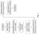
- FIG. 1 there is shown a schematic representation of the present invention as it relates to a fluxless solder ball mount assembly process module with a shortened assembly procedure which procedure will subsequently require a vertically configured heat treatment arrangement, as described in a sister application.
- a FOUP front operating unified pod container
- a liquid binder is applied to the upper surface of the wafer
- excess binder is driven off the chip by a curtain of compressed dry air leaving only a thin film thereon
- the wafer is coarsely adjusted with a pre-aligner robotic arm and loaded onto a vacuum support chuck
- an optomechanical system aligns the wafer precisely to one aligned fixed stencil
- solder balls are applied through holes in the stencil and onto binder coated pads on the wafer
- excess balls are removed with a further sweeping application of compressed dry air, the excess balls being retrieved by a vacuum suction system there adjacent
- the wafer is then optically inspected to confirm or if needed, correct ball placement.
- the properly loaded wafer would then be withdrawn by the robotic arm for subsequent treatment in a further module.
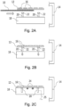
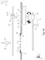
- FIG. 2A the side elevational view shown in figure 2A , wherein a robotic arm 10 is shown delivering a wafer 12 into a temperature and humidity controlled application chamber 14.
- the wafer 12 is preloaded with a plurality of solder ball receiving pads 16.
- a 3-independent-zone vacuum chuck 18 is also arranged within the application chamber (module) 14.
- a plurality of support pins 20 extends from the upper surface of the support chuck 18.
- the support pins 20 are vertically displaceable and have a vacuum cup 22 arranged on their uppermost or distal end, as may be seen in figures 2A and 2B .
- the robotic arm 10 deposits the wafer 12 onto the upper ends of the support pins 20, as represented in figure 2B .
- the support pins 20, carrying the wafer 12 are preferably pneumatically withdrawn fully into the vacuum chuck 18 and become recessed pins 20, as represented in figure 2C .
- a plurality of vacuum channels 24 arranged within the chuck 18 are actuated to hold the wafer 12 firmly in place.
- the vacuum channels 24 are grouped into three zones across the surface of the chuck 18 each of which zone may be controlled independently of one another, by a proper computer controlled circuit 25.
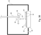
- FIG. 3A a side elevational view shows the application chamber 14 having a lower end whether the vacuum support chuck 18 residing thereat.
- a gantry frame 30 extends into and within the chamber 14, above the wafer 12, which is pre-loaded with its pads 16, the gantry frame 30 being movable controllably thereacross (either transversely or longitudinally, or both ways) thereacross by computer controlled servomotors.
- An array of binder spray nozzles 32 are arranged on the lower end of the gantry frame 30, enabled to spray a liquid binder "b" therethrough, via a conduit in the gantry frame 30 and onto the wafer 12 therebelow.
- An "air knife” 34 is also arranged on the lower end of the gantry frame 30, so as to also apply a computer controlled curtain of compressed dry air across the width of the wafer 12 thereinbelow, as necessary, by computer controlled movement of the gantry frame 30. Actuation of the gantry frame 30 scans the nozzles 32 and the air knife 34 over the wafer 12.
- Figure 3B shows the binder "b", being sprayed upon the pad loaded wafer 12, meaning both the wafer 12 and the pads 16, as the gantry frame 30 traverses the breath of the wafer 12 therebeneath. It is to be noted that the binder "b” is shown having an excessive accumulation on the wafer 12 and possibly on the pads 16, as viewed on the right hand side of figure 3B .
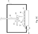
- Figure 3C represents the traversal of the gantry frame 30 above the binder coated wafer 12 therebeneath.
- the gantry frame 30 in figure 3C depicts the air knife 34, preferably comprised of an array of nozzles 92, (described further hereinbelow), sweeping a curtain of humidity and temperature controlled compressed dry air across the surface of the binder laden wafer 12 supported on the vacuum chuck 18.
- the compressed dry air may be blown perpendicular to or angled with respect to the horizontal surface of the wafer 12.
- the mechanical and/or evaporative action of the compressed dry air blown curtain or stream drives excess binder off of the wafer 12, as shown in the left hand side of the application chamber 14 and into a collection vessel (not shown) through a lower drain port 36 therewithin.
- a thin film of binder 38 shown on the wafer 12 on the right hand side of the wafer 12, is represented in figure 3C .
- the thickness of that thinned binder film 38 may be controlled by controlling the flow rate of the compressed dry air, the scan speed of the gantry frame 30, the position of the air knives 34 or their nozzle shapes.
- a side elevational view of the alignment process of the wafer 12, held by the vacuum support chuck 18, the wafer 12 and its respective pads 16 are all being represented in figure 4A , the pads 16 having received their thin film of binder "b".
- An alignment camera arrangement 40 is arranged within the application chamber 14, on a gantry frame arrangement 42, the camera arrangement 40 being movably controlled in the X and Y directions on that gantry frame arrangement 42, by servomotors 53 and 54.
- Each alignment camera 40 is comprised of a lens assembly, a light sensor or and an artificial light source.
- the vacuum support chuck 18 also shown in figure 4A is supported, and may be actuated by a multi-axis stage 56 in the X, Y, and Z directions and may be rotated in the theta direction (about the z-axis) through interaction by the control computer 52.
- the chuck 18 is 1 st positioned a vertical distance below the cameras 40 such that the wafer 12 is in focus as is shown in figure 4B .
- the cameras observe the wafer 12 through the alignment window, an opening 55 in the base plate 57.
- An alignment beam "I" represents the camera's "field of view” in figure 4A emanating from one of the pair of alignment cameras 40 directed downwardly onto the array of pads 16 therebeneath.
- a separately supported and controlled verification camera 62 is also shown in figure 4A to be described further hereinbelow.
- FIG 4B shows a pair of alignment cameras 40 mounted on a transverse beam 44 as part of the gantry frame 42, and are computer controlled so as to move independently on that transverse beam 44 in the X direction.
- the beam 44 itself is actuated in the Y direction, but is parallel to the X direction.
- Each camera 40 is preferably comprised of a lens assembly, a light sensor and artificial light source for this process of component alignment, the vacuum chuck 18 being initially positioned at a vertical distance below the cameras 40, such that the surface of the wafer 12 is in focus.
- Each camera 40 then is programmed to capture an image of a different position on the wafer 12 and sends these images to the control computer 50 via a proper circuit 52.
- This visual information is processed through the control computer 50, to indicate the precise position of the wafer 12 on the vacuum chuck 18.
- the stage 56 through circuit 52, actuates the chuck 18 as instructed to align the wafer 12 in the proper X, Y and Theta orientation, as represented in figure 4A such that only a single additional translation step is needed to align the pads 16 of the wafer 12 directly below corresponding holes 72 on a ball stencil 60, represented in figure 5 in figures 6A and 6B described hereinbelow.
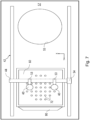
- a hole-laden or holed-ball stencil 60 shown in a side elevational view in figure 5 , arranged within the chamber 14 above a vacuum support chuck 18.
- the vacuum support chuck 18 shown movably controlled by a stage 56 thereunder.
- a downward looking verification camera 62 is shown mounted above the ball stencil 60.
- the verification camera 62 may be movable vertically by proper computer control in the "Z" direction with the pneumatic support arrangement 63.
- the wafer 12 is first translated in the "Y” direction from its position below the alignment camera arrangement 40 to a position directly below the ball stencil 60 and the verification camera 62.
- the wafer 12 on the chuck 18 is then translated in the "Z" direction such that it contacts or nearly contacts the bottom of the ball stencil 60.
- the ball stencil 60 and the wafer 12 are within the focal plane of the verification camera 62.
- the computer controlled verification camera 62 is instructed to take an image of a single location on the wafer 12.
- the control computer 50 uses this information to confirm the final alignment between the wafer 12 and the ball stencil 60. Once confirmed, the verification camera 62 is lifted up by controlled lift pneumatic driver 63 and out of the way of the ball mount head 70, shown hereinbelow in figures 6A and 6B and described therewith.
- each of these pads 16 should end up centered in the X and Y directions under one of the holes 72 in the ball stencil 60.
- the figure on the left, figure 6B shows the wafer 12 itself with a plurality of pads 16 neatly aligned thereon.
- Figure 6A on the right shows the wafer 12 itself with its plurality of pads 16.
- the stencil 60 represented in figure 6B has a similar neatly aligned array of holes 72 thereon. When the wafer 12 is in proper alignment, each of these pads 16 should end up centered in the X and Y directions under one of the holes 72 in the ball stencil 60.
- the verification camera 62 is then instructed by the control computer to take a picture of a subset of these aligned pad 16 and holes 72. If all of the pads 16 and holes 72 within the camera's field of view are determined by the control computer 50 to be in proper alignment, then the entire wafer 16 is presumed to be properly aligned.
- Figure 7 displays the alignment process, wherein during the setup of the tool, before processing begins, the gantry frame 42 positions the two alignment cameras 40 over the stencil 60.
- the stencil 60 is held in a fixed position on the base plate 57 and remains fixed throughout its setup and processing.
- the stencil 60 contains a plurality of holes 72 and a unique hole pattern corresponding to the particular wafer 12 which will be processed. While each camera 40 (both of them) is over the stencil 60, each captures an image of the part of the stencil 60, which image is a section of the overall pattern of holes 72.
- These image sections are identified in figure 9 as stencil image # 1 (92) and stencil image #2 (94). These image sections 92 and 94 are sent to the control computer 50 for storage and analysis.
- Each image captures a number of stencil holes 72 as shown in figure 10 .
- the number of holes 72 may be in the hundreds.
- this and software identifies a subset of holes 96 within the image 92 or 94 which form a unique pattern which will be referred to as a "composite feature".
- the vision software determines the precise position and orientation of the composite feature. The result is that during training, software identifies and memorizes the precise position of the two composite features on the stencil 60 in terms of a global coordinate system. This "global coordinate" is fixed with respect to stationary elements of the tool such as the base plate 57.
- the gantry frame 44 then positions the alignment cameras 40 and 40 over the alignment window 55 as shown in figure 8 .
- the camera positions are then locked in place and remain fixed all during processing and production of the wafer 12.
- a wafer 12 is loaded onto the support chuck 18 as represented in figure 4A and positioned under the alignment cameras 40 and 40.
- the wafer 12 contains a plurality of pads 16.
- Each camera 40 and 40 captures an image of part of the wafer 12, a section of the overall pad pattern. These image sections identified in figure 9 is wafer image # 1 (93) and wafer image # 2 (95). These images are then sent to the control computer 50 for analysis.
- Each image 93 and 95 may capture as many or more pads 16 as shown in figure 10 .
- the vision software identifies a subset of pads 96 within the image 93 and/or 95 which form a unique pattern, a "composite feature' like that on the stencil 60.
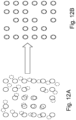
- the vision software now compares stencil image #1 (92) to wafer image # 1 (93) and stencil image # 2 (94) to wafer image #2 (95), this comparison being represented in figure 11 .
- the software calculates the X, Y, Z and Theta motions that the support chuck 18 must make such of the final positions and orientations of each pair of the wafer stencil composite features will match as shown in figure 12B , the control computer 50 through the proper circuit 52, then commands the support chuck 18 to execute these calculated motions.
- the wafer 12 is thus aligned and brought upwardly near or into contact with the bottom of the stencil 60.
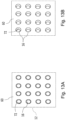
- the verification camera 62 captures a single image of the stencil 60 and the wafer 12. This image is labeled "verification image” and 97 as represented in figure 9 . As with the alignment cameras 40 and 40, the verification camera 62 captures a subset of the overall hole - pad pattern. The verification camera 62 sends this image to the control computer 50 where the vision software identifies the holes 72 and the pads 16 in that image. The vision software calculates the center of each pad 16 and of each hole 72, and compares them.
- the software program determines whether the final alignment of the wafer 12 and stencil 60 is good as the verification image shown in figure 13A or as bad as he verification image shown in figure 13B . If the wafer 12 and the stencil 16 are perfectly aligned, the center of each pad 16 will match the center of a hole 72 as shown by the verification image shown in figure 13A .
- the ball mounting process is represented in figure 14 , wherein the wafer 12 has been raised up to the bottom of the stencil 60, as represented in figures 14 and 15 .
- the ball mount head 70 is robotically brought into the application chamber 14 through a side thereof, and is controllably lowered into proximity of the holes 72 in the stencil 60, the ball mount head 70 being computer controlled by a "coarse” "Y” direction pneumatic control arrangement 78 and a “Z” direction pneumatic control arrangement 80.
- a “fine” “Y” direction pneumatic control arrangement 74 represented in figure 14 , is discussed further hereinbelow.
- the coarse "Y” direction pneumatic control arrangement 78 moves the ball mount head 70 out of the way of the verification camera 62.
- the ball mount head 70 in one preferred embodiment is an array of transversely extending sweep members 82, in one preferred embodiment, consisting of thin coils or loops of wire 83, attached onto the underside of the ball mount head 70.
- thin flexible brushes (not shown for clarity of the drawings) replace the coils or loops of wire 83 on the underside of the ball mount head 70.
- Those sweep members 82 or more specifically, those loops of wires 83 underneath the ball mount head 70 nearly contact or just barely contact the stencil 60.
- a reservoir 84 within the ball mount head 70 is programmed to release a volume of solder balls 86 which is thus dispersed across the upper surface of the stencil 60.
- a wave generator 88 is actuated by the control computer 50 through the proper circuit 52, to begin vibrating the sweep members 82, preferably loops of wire 83, in brushing contact with the solder balls 86 on the surface of the stencil 60.
- the brushing vibration of the wires 83 (or sweep member 82 brushes) contact the solder balls 86 and the vibration of the wires 83 results in movement of the solder balls 86.
- the solder balls move over the stencil 60, they drop through the holes 72 in the stencil, and stick to the binder "b" coated wafer pads 16 properly arrayed therebeneath.
- Distribution of the solder balls 86 and filling of the holes 72 in the stencil 60 is further encouraged by oscillating the wires back and forth a different dimension, as for example, only several millimeters of oscillation using the fine "Y" pneumatic controlled driver 74 mounted on the ball mount head 70, in conjunction with the other separate drivers 78 and 80, again, represented in figure 14 mounted on the ball mounted head 70.
- the ball mount head 70 is controllably effected to move up and out of the way of the compressed dry air sweep detailed hereinbelow in figure 15 .
- solder ball sweep and recovery discussed earlier is shown again in figure 15 .
- the air knife 34 is actuated to sweep over the surface of the solder ball laden stencil 60, thus effecting a curtain of compressed dry air from its nozzles 92, as the air knife 34 is caused to move as it is carried by a pneumatically driven arm 94.
- solder balls 86 not properly secured to a binder "b" on a pad 16 on the wafer 12 are driven before the curtain of compressed dry air sweeping across the solder ball laden stencil 60, effecting loose solder balls 86 towards a vacuum and collection vessel 90 at the downstream end of the compressed dry air sweep process.
- those solder balls 86 which did not fall into a receiving hole 72 in the stencil 60 are swept along before the air knife 34 (the compressed dry air nozzle arrangement 92) into capture by that collection vessel 90.
- Those solder balls 86 may be reused in further processing of additional wafers.
- Optical inspection of the finally assembled wafer 12 is represented in figure 16 .
- the wafer 12 having its proper array of pads 16 and multiple solder balls 86 is borne by the vacuum support chuck 18.
- a (line scan) camera 98 utilized for alignment scanning, comprising a lens assembly, a light sensor in an artificial light source, is arrayed downwardly while the vacuum support chuck 18 therebeneath supports the movement of the assembled wafer 12 through the field of view of the line scan camera 98 to create a composite image of the entire wafer 12.
- This image is processed by the control computer 50 confirming the alignment each solder ball 86 on the wafer 12 to determine if there are any missing or extra solder balls 86 which may have to be taken care of.
- a further embodiment of the present invention includes the multiple cameras described hereinabove by a single set of optics (cameras) to provide for both alignment and final inspection.
Landscapes
- Engineering & Computer Science (AREA)
- Physics & Mathematics (AREA)
- General Physics & Mathematics (AREA)
- Computer Vision & Pattern Recognition (AREA)
- Theoretical Computer Science (AREA)
- Microelectronics & Electronic Packaging (AREA)
- Computer Hardware Design (AREA)
- Power Engineering (AREA)
- Manufacturing & Machinery (AREA)
- Quality & Reliability (AREA)
- Condensed Matter Physics & Semiconductors (AREA)
- Container, Conveyance, Adherence, Positioning, Of Wafer (AREA)
- Electric Connection Of Electric Components To Printed Circuits (AREA)
- Robotics (AREA)
Claims (14)
- - Système pour le traitement sans flux d'une pluralité de billes de soudure (86) sur une plaquette (12) dans une chambre de confinement de procédé de traitement de plaquette (14), le système comprenant la chambre de confinement de procédé de traitement de plaquette (14) et comprenant :
un mandrin de support à vide articulable (18) pour maintenir un support d'une plaquette (12) contenant une pluralité de billes de soudure (86) à mesure que la plaquette est traitée à l'intérieur de la chambre de confinement de procédé (14) ;
caractérisé par le fait que le système comprend en outre :un applicateur de liant sans flux articulable (32) disposé en relation de dépôt de liant au-dessus de la plaquette (12) à l'intérieur de la chambre de confinement de procédé (14) ; etun distributeur de rideau de fluide articulable (34) disposé en relation de traitement de minimisation d'excès d'application de liant par rapport à tout liant sans flux (38) appliqué sur la plaquette (12) à l'intérieur de la chambre de confinement de procédé (14) pour appliquer un rideau de fluide sur la plaquette, le rideau de fluide étant de l'air comprimé. - - Système selon la revendication 1, dans lequel le distributeur de rideau de fluide articulable (34) comprend un réseau de buses d'éjection d'air (92) disposées de manière mobile au-dessus de la plaquette (12) en cours de traitement.
- - Système selon la revendication 2, dans lequel les buses d'éjection d'air (92) et l'applicateur de liant sans flux articulable (32) sont tous deux supportés sur un agencement de bâti de portique commun (42).
- - Système selon la revendication 1, comprenant une cuve (90) de collecte de billes de soudure en excès utilisant du vide et disposée adjacente à la plaquette (12) en cours de traitement pour collecter toute bille de soudure (86) en excès qui n'est pas correctement disposée sur la plaquette.
- - Système selon la revendication 1, comprenant un agencement de caméra (40) apte à être introduit à l'intérieur de la chambre de confinement de procédé (14) pour inspecter et analyser la plaquette (12) traitée pour une précision de mise en place de billes de soudure après le retrait de billes de soudure (86) en excès par la cuve (90) de collecte de billes de soudure en excès.
- - Système selon la revendication 1, dans lequel il y a une pluralité de canaux de vide (24) disposés à l'intérieur du mandrin de support à vide articulable (18) configurés pour maintenir la plaquette (12) fermement en place, les canaux de vide étant regroupés en trois zones à travers la surface du mandrin.
- - Système selon la revendication 6, comprenant en outre un circuit contrôlé par ordinateur convenable (25), dans lequel chacune desdites zones des canaux de vide (24) peut être contrôlée indépendamment les unes des autres, par le circuit contrôlé par ordinateur convenable.
- - Système selon la revendication 6 ou la revendication 7, comprenant en outre un réseau de broches de support (20) mobiles verticalement pour porter la plaquette (12), qui s'étendent à partir d'une surface supérieure du mandrin de support à vide articulable (18), chaque broche de support ayant une ventouse (22) disposée sur une extrémité la plus haute ou distale de la broche de support.
- - Système selon la revendication 8, dans lequel les broches de support (20) sont configurées pour être rétractées dans le mandrin à vide articulable (18) afin de permettre l'abaissement de la plaquette (12) sur le mandrin à vide.
- - Système selon la revendication 9, comprenant en outre un appareil de contrôle de broches pneumatique pour permettre l'abaissement de la plaquette (12) d'une manière contrôlée, ce par quoi les broches de support (20) sont retirées pneumatiquement entièrement dans le mandrin à vide (18) pour devenir des broches en retrait.
- - Procédé d'utilisation du système selon l'une quelconque des revendications précédentes pour appliquer un liant sans flux (38) à une pluralité de billes de soudure (86) sur une plaquette (12) dans une chambre de confinement de procédé de traitement de plaquette (14), comprenant les étapes :utiliser le mandrin de support à vide articulable (18) pour maintenir un support d'une plaquette (12) contenant une pluralité de billes de soudure (86) à mesure que la plaquette est traitée à l'intérieur de la chambre de confinement de procédé (14) ;utiliser l'applicateur de liant sans flux articulable (32) disposé en relation de dépôt de liant au-dessus de la plaquette (12) à l'intérieur de la chambre de confinement de procédé (14) pour déposer un liant sans flux (38) sur une surface supérieure de ladite plaquette ; etutiliser le distributeur de rideau de fluide articulable (34) disposé en relation de traitement de minimisation d'application de liant par rapport audit liant sans flux (38) appliqué à la plaquette (12) à l'intérieur de la chambre de confinement de procédé (14) pour appliquer un rideau de fluide sur la plaquette, le rideau de fluide étant de l'air comprimé.
- - Procédé de traitement d'une pluralité de billes de soudure (86) sur une plaquette (12) dans une chambre de confinement de traitement de plaquette (14), le procédé comprenant :lever une plaquette (12) chargée de plots par un bras robotique (10) dans la chambre de confinement de traitement de plaquette (14) ;supporter la plaquette (12) chargée de plots à l'intérieur de la chambre de confinement de traitement de plaquette (14) par une pluralité de broches de support (20) mobiles verticalement s'étendant à partir d'un mandrin à vide articulable (18) disposé à l'intérieur de la chambre de confinement de traitement de plaquette ;fixer la plaquette (12) chargée de plots sur une pluralité de ventouses (22) disposées chacune sur l'extrémité la plus haute ou distale des broches de support (20) mobiles verticalement, par un vide à l'intérieur de celles-ci ;rétracter les broches de support (20) mobiles dans le mandrin à vide articulable (18) ;appliquer un vide supplémentaire à partir d'une pluralité de canaux de vide (24) dans le mandrin à vide articulable (18), sur un côté inférieur de la plaquette (12) chargée de plots pour fixer la plaquette chargée de plots à celui-ci ;déposer un liant sans flux (38) sur une surface supérieure de la plaquette (12) chargée de plots et supportée sur le mandrin à vide articulable (18) ;souffler un rideau d'air sec comprimé sur la surface supérieure chargée de liant de la plaquette (12) chargée de plots ;disposer un pochoir chargé de trous (60) sur la plaquette (12) chargée de plots ;déplacer la plaquette (12) chargée de plots sous le pochoir chargé de trous (60) ;faire tomber une pluralité de billes de soudure (86) à partir d'une tête de montage de billes supportée au-dessus de la plaquette (12) chargée de plots et sur la plaquette (12) chargée de plots ;souffler un autre rideau d'air sec comprimé sur les billes de soudure (86) sur la plaquette (12) pour renforcer les billes de soudure sur la plaquette et pour éliminer des billes de soudure en excès sur la plaquette ; etaspirer et collecter des billes de soudure (86) en excès à partir de la plaquette (12) chargée de plots, qui ne sont pas alignées dans le pochoir chargé de trous (60) ; etretirer la plaquette (12) chargée de plots de la chambre de confinement de traitement de plaquette chargée de plots (14) pour un traitement dans une autre chambre de traitement.
- - Procédé selon la revendication 12, comprenant l'étape :abaisser un agencement de balayage vibratoire (82, 83) à un emplacement situé au-dessus de la plaquette (12) chargée de plots à l'intérieur de la chambre de confinement de traitement de plaquette (14) ;faire vibrer l'agencement de balayage (82, 83) au-dessus de la plaquette (12) chargée de plots avec ses billes de soudure (86) sur celle-ci afin d'assurer un mise en place de billes de soudure à l'intérieur d'un trou (72) dans le pochoir chargé de trous (60).
- - Procédé selon la revendication 13, comprenant l'étape :
appliquer un vide le long d'un bord du pochoir (60) pour permettre une collecte de billes de soudure (86) en excès à partir de la plaquette (12) chargée de plots.
Applications Claiming Priority (3)
| Application Number | Priority Date | Filing Date | Title |
|---|---|---|---|
| US201762605277P | 2017-08-07 | 2017-08-07 | |
| PCT/US2018/045473 WO2019032485A1 (fr) | 2017-08-07 | 2018-08-07 | Agencement de montage de bille de soudure sans flux |
| EP18843170.4A EP3665717B1 (fr) | 2017-08-07 | 2018-08-07 | Agencement de montage de bille de soudure sans flux |
Related Parent Applications (1)
| Application Number | Title | Priority Date | Filing Date |
|---|---|---|---|
| EP18843170.4A Division EP3665717B1 (fr) | 2017-08-07 | 2018-08-07 | Agencement de montage de bille de soudure sans flux |
Publications (4)
| Publication Number | Publication Date |
|---|---|
| EP4099366A2 EP4099366A2 (fr) | 2022-12-07 |
| EP4099366A3 EP4099366A3 (fr) | 2023-02-15 |
| EP4099366C0 EP4099366C0 (fr) | 2024-12-11 |
| EP4099366B1 true EP4099366B1 (fr) | 2024-12-11 |
Family
ID=65229959
Family Applications (2)
| Application Number | Title | Priority Date | Filing Date |
|---|---|---|---|
| EP22178977.9A Active EP4099366B1 (fr) | 2017-08-07 | 2018-08-07 | Système pour le traitement sans flux d'une pluralité de billes de soudure sur une tranche |
| EP18843170.4A Active EP3665717B1 (fr) | 2017-08-07 | 2018-08-07 | Agencement de montage de bille de soudure sans flux |
Family Applications After (1)
| Application Number | Title | Priority Date | Filing Date |
|---|---|---|---|
| EP18843170.4A Active EP3665717B1 (fr) | 2017-08-07 | 2018-08-07 | Agencement de montage de bille de soudure sans flux |
Country Status (6)
| Country | Link |
|---|---|
| US (1) | US10879102B2 (fr) |
| EP (2) | EP4099366B1 (fr) |
| JP (1) | JP7084981B2 (fr) |
| KR (1) | KR102353167B1 (fr) |
| CN (1) | CN111095504B (fr) |
| WO (1) | WO2019032485A1 (fr) |
Families Citing this family (10)
| Publication number | Priority date | Publication date | Assignee | Title |
|---|---|---|---|---|
| CN108022865B (zh) * | 2017-11-16 | 2019-09-20 | 北京创昱科技有限公司 | 晶片定位及装载系统 |
| KR102752911B1 (ko) * | 2018-09-28 | 2025-01-10 | 보스턴 프로세스 테크놀로지스, 아이엔씨. | 다중 모듈 칩 제조 장치 |
| JP7220554B2 (ja) * | 2018-12-04 | 2023-02-10 | 東京エレクトロン株式会社 | プローブ装置、及び、プローブ装置の調整方法 |
| TWI889679B (zh) * | 2019-04-30 | 2025-07-11 | 日商迪睿合股份有限公司 | 對滑動對象物之表面提供或排除滑動處理物之方法 |
| EP3968359A4 (fr) * | 2019-05-08 | 2023-01-25 | Tokyo Electron Limited | Dispositif, système et procédé de liaison |
| US11440117B2 (en) * | 2019-09-27 | 2022-09-13 | Jian Zhang | Multiple module chip manufacturing arrangement |
| KR102249384B1 (ko) * | 2020-07-17 | 2021-05-06 | 정관식 | 플럭스 프리 플립칩 패키지 제조장치 및 제조방법 |
| KR102661443B1 (ko) * | 2020-09-10 | 2024-04-30 | 세메스 주식회사 | 기판 처리 장치, 잉크젯 장치 및 메인터넌스 방법 |
| PH12022050163A1 (en) * | 2021-05-18 | 2023-04-17 | Inari Tech Sdn Bhd | Apparatus, system and method for determining a match condition for a printed circuit board to a stencil |
| US12512431B2 (en) | 2023-02-17 | 2025-12-30 | Air Products And Chemicals, Inc. | Apparatus and method for wafer oxide removal and reflow treatment |
Family Cites Families (29)
| Publication number | Priority date | Publication date | Assignee | Title |
|---|---|---|---|---|
| US5468681A (en) * | 1989-08-28 | 1995-11-21 | Lsi Logic Corporation | Process for interconnecting conductive substrates using an interposer having conductive plastic filled vias |
| US5431332A (en) * | 1994-02-07 | 1995-07-11 | Motorola, Inc. | Method and apparatus for solder sphere placement using an air knife |
| US5872051A (en) * | 1995-08-02 | 1999-02-16 | International Business Machines Corporation | Process for transferring material to semiconductor chip conductive pads using a transfer substrate |
| JPH09232742A (ja) * | 1996-02-28 | 1997-09-05 | Hitachi Ltd | 電子回路装置の製造方法 |
| US6869008B2 (en) * | 1998-05-29 | 2005-03-22 | Hitachi, Ltd. | Method of forming bumps |
| JP3561166B2 (ja) * | 1999-01-21 | 2004-09-02 | 株式会社リコー | 異方性導電ペーストを用いた電子部品の接続方法 |
| JP3619410B2 (ja) * | 1999-11-18 | 2005-02-09 | 株式会社ルネサステクノロジ | バンプ形成方法およびそのシステム |
| US7632750B2 (en) * | 2006-07-07 | 2009-12-15 | Semigear Inc | Arrangement for solder bump formation on wafers |
| TWI273666B (en) * | 2004-06-30 | 2007-02-11 | Athlete Fa Corp | Method and device for mounting conductive ball |
| US7918383B2 (en) * | 2004-09-01 | 2011-04-05 | Micron Technology, Inc. | Methods for placing substrates in contact with molten solder |
| TWI413471B (zh) * | 2006-01-27 | 2013-10-21 | 揖斐電股份有限公司 | Method and device for mounting solder ball |
| JP4896778B2 (ja) * | 2007-03-13 | 2012-03-14 | アスリートFa株式会社 | 搭載装置およびその制御方法 |
| JP5183250B2 (ja) * | 2007-04-16 | 2013-04-17 | アスリートFa株式会社 | マスクおよびこのマスクを用いたプリント配線板の製造方法 |
| JP5098434B2 (ja) * | 2007-05-21 | 2012-12-12 | 株式会社日立プラントテクノロジー | ハンダボール印刷装置 |
| JP2009253018A (ja) * | 2008-04-07 | 2009-10-29 | Shinkawa Ltd | ボンディング装置及びボンディング方法 |
| US7780063B2 (en) * | 2008-05-15 | 2010-08-24 | International Business Machines Corporation | Techniques for arranging solder balls and forming bumps |
| JP2010129929A (ja) * | 2008-11-28 | 2010-06-10 | Canon Inc | 基板保持装置、基板保持方法、露光装置およびデバイス製造方法 |
| JP2009071332A (ja) * | 2008-12-15 | 2009-04-02 | Athlete Fa Kk | 導電性ボールを搭載するための装置 |
| JP5251699B2 (ja) * | 2009-04-23 | 2013-07-31 | 株式会社日立プラントテクノロジー | ハンダボール印刷装置およびハンダボール印刷方法 |
| JP5206572B2 (ja) * | 2009-04-23 | 2013-06-12 | 株式会社日立プラントテクノロジー | ハンダボール印刷装置 |
| KR101044135B1 (ko) * | 2009-11-30 | 2011-06-28 | 삼성전기주식회사 | 인쇄회로기판의 제조방법 |
| CN102610535B (zh) * | 2011-01-21 | 2014-07-09 | 三星半导体(中国)研究开发有限公司 | 植球装置、焊球拾取方法以及焊球安装方法 |
| DE102011013172A1 (de) * | 2011-02-28 | 2012-08-30 | Fraunhofer-Gesellschaft zur Förderung der angewandten Forschung e.V. | Paste zum Verbinden von Bauteilen elektronischer Leistungsmodule, System und Verfahren zum Auftragen der Paste |
| US8921221B2 (en) * | 2011-06-20 | 2014-12-30 | International Business Machines Corporation | IMS (injection molded solder) with two resist layers forming solder bumps on substrates |
| US20130147129A1 (en) * | 2011-12-08 | 2013-06-13 | Nan Ya Technology Corporation | Wafer supporting structure |
| WO2014007758A1 (fr) * | 2012-07-03 | 2014-01-09 | Heptagon Micro Optics Pte. Ltd. | Utilisation de mandrins à dépression afin de maintenir une plaquette ou une pile secondaire de plaquette |
| US20150034702A1 (en) * | 2013-08-01 | 2015-02-05 | Semigear Inc | Apparatus & method for treating substrate |
| JP6567290B2 (ja) * | 2015-02-20 | 2019-08-28 | Aiメカテック株式会社 | 基板処理装置、基板処理システム、及び基板処理方法 |
| WO2016174966A1 (fr) * | 2015-04-27 | 2016-11-03 | アスリートFa株式会社 | Élément de type fil en faisceau, tête de transfert à billes, dispositif de chargement de billes, et procédé de chargement de billes |
-
2018
- 2018-08-01 US US15/998,298 patent/US10879102B2/en active Active
- 2018-08-07 EP EP22178977.9A patent/EP4099366B1/fr active Active
- 2018-08-07 JP JP2020505168A patent/JP7084981B2/ja active Active
- 2018-08-07 KR KR1020207006038A patent/KR102353167B1/ko active Active
- 2018-08-07 CN CN201880052055.3A patent/CN111095504B/zh active Active
- 2018-08-07 WO PCT/US2018/045473 patent/WO2019032485A1/fr not_active Ceased
- 2018-08-07 EP EP18843170.4A patent/EP3665717B1/fr active Active
Also Published As
| Publication number | Publication date |
|---|---|
| EP3665717B1 (fr) | 2022-06-15 |
| CN111095504A (zh) | 2020-05-01 |
| EP3665717A1 (fr) | 2020-06-17 |
| JP7084981B2 (ja) | 2022-06-15 |
| KR102353167B1 (ko) | 2022-01-19 |
| EP4099366C0 (fr) | 2024-12-11 |
| CN111095504B (zh) | 2023-07-07 |
| EP3665717A4 (fr) | 2021-05-19 |
| US10879102B2 (en) | 2020-12-29 |
| EP4099366A3 (fr) | 2023-02-15 |
| JP2020530197A (ja) | 2020-10-15 |
| KR20200037331A (ko) | 2020-04-08 |
| WO2019032485A1 (fr) | 2019-02-14 |
| EP4099366A2 (fr) | 2022-12-07 |
| US20190043745A1 (en) | 2019-02-07 |
Similar Documents
| Publication | Publication Date | Title |
|---|---|---|
| EP4099366B1 (fr) | Système pour le traitement sans flux d'une pluralité de billes de soudure sur une tranche | |
| US9318361B2 (en) | Collet cleaning method and die bonder using the same | |
| US11440117B2 (en) | Multiple module chip manufacturing arrangement | |
| EP3857592B1 (fr) | Agencement de fabrication de puces à modules multiples | |
| WO2015038074A1 (fr) | Système et procédé permettant de positionner une puce semi-conductrice avec une tête de liaison, système et procédé de liaison thermique | |
| JP5375133B2 (ja) | 部品実装装置 | |
| JP5120205B2 (ja) | 電子部品実装装置 | |
| KR20110050547A (ko) | 픽앤드플레이스 장치 | |
| KR101456138B1 (ko) | 레이저 칩 본딩기의 칩 공급장치 | |
| KR100576406B1 (ko) | 플럭스 저장장치 및 플럭스 전사방법 | |
| JP3661658B2 (ja) | 電子部品搭載装置および電子部品搭載方法 | |
| JP4896778B2 (ja) | 搭載装置およびその制御方法 | |
| JP2002111197A (ja) | 部品交換方法および部品交換装置 | |
| JP2021089949A (ja) | 導電性粒体搭載基板の不要物除去装置 | |
| JP7101497B2 (ja) | 作業装置および相対位置関係特定方法 | |
| JP2005197758A (ja) | 電子部品搭載装置および電子部品搭載方法 | |
| KR20250165351A (ko) | 실장 장치 | |
| WO2024232049A1 (fr) | Dispositif d'aide à la production et procédé d'aide à la production | |
| JP2025050553A (ja) | 部品搭載装置および部品搭載方法 | |
| JP2001007126A (ja) | ヘッドとワークの位置決め装置及び位置決め方法 |
Legal Events
| Date | Code | Title | Description |
|---|---|---|---|
| PUAI | Public reference made under article 153(3) epc to a published international application that has entered the european phase |
Free format text: ORIGINAL CODE: 0009012 |
|
| STAA | Information on the status of an ep patent application or granted ep patent |
Free format text: STATUS: THE APPLICATION HAS BEEN PUBLISHED |
|
| AC | Divisional application: reference to earlier application |
Ref document number: 3665717 Country of ref document: EP Kind code of ref document: P |
|
| AK | Designated contracting states |
Kind code of ref document: A2 Designated state(s): AL AT BE BG CH CY CZ DE DK EE ES FI FR GB GR HR HU IE IS IT LI LT LU LV MC MK MT NL NO PL PT RO RS SE SI SK SM TR |
|
| PUAL | Search report despatched |
Free format text: ORIGINAL CODE: 0009013 |
|
| AK | Designated contracting states |
Kind code of ref document: A3 Designated state(s): AL AT BE BG CH CY CZ DE DK EE ES FI FR GB GR HR HU IE IS IT LI LT LU LV MC MK MT NL NO PL PT RO RS SE SI SK SM TR |
|
| RIC1 | Information provided on ipc code assigned before grant |
Ipc: H01L 21/67 20060101ALI20230110BHEP Ipc: H01L 21/60 19740701ALI20230110BHEP Ipc: C25D 5/02 19740701ALI20230110BHEP Ipc: B23K 31/02 19680901ALI20230110BHEP Ipc: B23K 1/20 19680901ALI20230110BHEP Ipc: H05K 3/12 19680901ALI20230110BHEP Ipc: H01L 21/48 19740701ALI20230110BHEP Ipc: H01L 21/3213 19950101AFI20230110BHEP |
|
| STAA | Information on the status of an ep patent application or granted ep patent |
Free format text: STATUS: REQUEST FOR EXAMINATION WAS MADE |
|
| 17P | Request for examination filed |
Effective date: 20230815 |
|
| RBV | Designated contracting states (corrected) |
Designated state(s): AL AT BE BG CH CY CZ DE DK EE ES FI FR GB GR HR HU IE IS IT LI LT LU LV MC MK MT NL NO PL PT RO RS SE SI SK SM TR |
|
| RAP1 | Party data changed (applicant data changed or rights of an application transferred) |
Owner name: SHARPACK TECHNOLOGY PTE. LTD. |
|
| GRAP | Despatch of communication of intention to grant a patent |
Free format text: ORIGINAL CODE: EPIDOSNIGR1 |
|
| STAA | Information on the status of an ep patent application or granted ep patent |
Free format text: STATUS: GRANT OF PATENT IS INTENDED |
|
| INTG | Intention to grant announced |
Effective date: 20240702 |
|
| GRAS | Grant fee paid |
Free format text: ORIGINAL CODE: EPIDOSNIGR3 |
|
| GRAA | (expected) grant |
Free format text: ORIGINAL CODE: 0009210 |
|
| STAA | Information on the status of an ep patent application or granted ep patent |
Free format text: STATUS: THE PATENT HAS BEEN GRANTED |
|
| AC | Divisional application: reference to earlier application |
Ref document number: 3665717 Country of ref document: EP Kind code of ref document: P |
|
| AK | Designated contracting states |
Kind code of ref document: B1 Designated state(s): AL AT BE BG CH CY CZ DE DK EE ES FI FR GB GR HR HU IE IS IT LI LT LU LV MC MK MT NL NO PL PT RO RS SE SI SK SM TR |
|
| REG | Reference to a national code |
Ref country code: GB Ref legal event code: FG4D |
|
| REG | Reference to a national code |
Ref country code: CH Ref legal event code: EP |
|
| REG | Reference to a national code |
Ref country code: IE Ref legal event code: FG4D |
|
| REG | Reference to a national code |
Ref country code: DE Ref legal event code: R096 Ref document number: 602018077637 Country of ref document: DE |
|
| U01 | Request for unitary effect filed |
Effective date: 20241213 |
|
| U07 | Unitary effect registered |
Designated state(s): AT BE BG DE DK EE FI FR IT LT LU LV MT NL PT RO SE SI Effective date: 20250102 |
|
| PG25 | Lapsed in a contracting state [announced via postgrant information from national office to epo] |
Ref country code: HR Free format text: LAPSE BECAUSE OF FAILURE TO SUBMIT A TRANSLATION OF THE DESCRIPTION OR TO PAY THE FEE WITHIN THE PRESCRIBED TIME-LIMIT Effective date: 20241211 |
|
| PG25 | Lapsed in a contracting state [announced via postgrant information from national office to epo] |
Ref country code: ES Free format text: LAPSE BECAUSE OF FAILURE TO SUBMIT A TRANSLATION OF THE DESCRIPTION OR TO PAY THE FEE WITHIN THE PRESCRIBED TIME-LIMIT Effective date: 20241211 |
|
| PG25 | Lapsed in a contracting state [announced via postgrant information from national office to epo] |
Ref country code: NO Free format text: LAPSE BECAUSE OF FAILURE TO SUBMIT A TRANSLATION OF THE DESCRIPTION OR TO PAY THE FEE WITHIN THE PRESCRIBED TIME-LIMIT Effective date: 20250311 |
|
| PG25 | Lapsed in a contracting state [announced via postgrant information from national office to epo] |
Ref country code: GR Free format text: LAPSE BECAUSE OF FAILURE TO SUBMIT A TRANSLATION OF THE DESCRIPTION OR TO PAY THE FEE WITHIN THE PRESCRIBED TIME-LIMIT Effective date: 20250312 |
|
| PG25 | Lapsed in a contracting state [announced via postgrant information from national office to epo] |
Ref country code: RS Free format text: LAPSE BECAUSE OF FAILURE TO SUBMIT A TRANSLATION OF THE DESCRIPTION OR TO PAY THE FEE WITHIN THE PRESCRIBED TIME-LIMIT Effective date: 20250311 |
|
| PG25 | Lapsed in a contracting state [announced via postgrant information from national office to epo] |
Ref country code: SM Free format text: LAPSE BECAUSE OF FAILURE TO SUBMIT A TRANSLATION OF THE DESCRIPTION OR TO PAY THE FEE WITHIN THE PRESCRIBED TIME-LIMIT Effective date: 20241211 |
|
| PG25 | Lapsed in a contracting state [announced via postgrant information from national office to epo] |
Ref country code: PL Free format text: LAPSE BECAUSE OF FAILURE TO SUBMIT A TRANSLATION OF THE DESCRIPTION OR TO PAY THE FEE WITHIN THE PRESCRIBED TIME-LIMIT Effective date: 20241211 |
|
| PG25 | Lapsed in a contracting state [announced via postgrant information from national office to epo] |
Ref country code: IS Free format text: LAPSE BECAUSE OF FAILURE TO SUBMIT A TRANSLATION OF THE DESCRIPTION OR TO PAY THE FEE WITHIN THE PRESCRIBED TIME-LIMIT Effective date: 20250411 |
|
| PG25 | Lapsed in a contracting state [announced via postgrant information from national office to epo] |
Ref country code: SK Free format text: LAPSE BECAUSE OF FAILURE TO SUBMIT A TRANSLATION OF THE DESCRIPTION OR TO PAY THE FEE WITHIN THE PRESCRIBED TIME-LIMIT Effective date: 20241211 |
|
| PG25 | Lapsed in a contracting state [announced via postgrant information from national office to epo] |
Ref country code: CZ Free format text: LAPSE BECAUSE OF FAILURE TO SUBMIT A TRANSLATION OF THE DESCRIPTION OR TO PAY THE FEE WITHIN THE PRESCRIBED TIME-LIMIT Effective date: 20241211 |
|
| U20 | Renewal fee for the european patent with unitary effect paid |
Year of fee payment: 8 Effective date: 20250827 |
|
| PLBE | No opposition filed within time limit |
Free format text: ORIGINAL CODE: 0009261 |
|
| STAA | Information on the status of an ep patent application or granted ep patent |
Free format text: STATUS: NO OPPOSITION FILED WITHIN TIME LIMIT |
|
| 26N | No opposition filed |
Effective date: 20250912 |