EP4089736A1 - Verfahren zur herstellung einer back-thinned-festkörperbildgebungsvorrichtung - Google Patents
Verfahren zur herstellung einer back-thinned-festkörperbildgebungsvorrichtung Download PDFInfo
- Publication number
- EP4089736A1 EP4089736A1 EP21744437.1A EP21744437A EP4089736A1 EP 4089736 A1 EP4089736 A1 EP 4089736A1 EP 21744437 A EP21744437 A EP 21744437A EP 4089736 A1 EP4089736 A1 EP 4089736A1
- Authority
- EP
- European Patent Office
- Prior art keywords
- semiconductor layer
- region
- state imaging
- asperity
- front surface
- Prior art date
- Legal status (The legal status is an assumption and is not a legal conclusion. Google has not performed a legal analysis and makes no representation as to the accuracy of the status listed.)
- Pending
Links
- 238000003384 imaging method Methods 0.000 title claims abstract description 74
- 238000000034 method Methods 0.000 title claims abstract description 35
- 238000004519 manufacturing process Methods 0.000 title claims abstract description 34
- 239000004065 semiconductor Substances 0.000 claims abstract description 103
- 238000005530 etching Methods 0.000 claims abstract description 27
- 239000000758 substrate Substances 0.000 claims description 19
- 230000003647 oxidation Effects 0.000 claims description 11
- 238000007254 oxidation reaction Methods 0.000 claims description 11
- 238000009825 accumulation Methods 0.000 claims description 10
- 238000005498 polishing Methods 0.000 claims description 7
- 239000010410 layer Substances 0.000 description 90
- BJQHLKABXJIVAM-UHFFFAOYSA-N bis(2-ethylhexyl) phthalate Chemical compound CCCCC(CC)COC(=O)C1=CC=CC=C1C(=O)OCC(CC)CCCC BJQHLKABXJIVAM-UHFFFAOYSA-N 0.000 description 8
- 238000002955 isolation Methods 0.000 description 7
- 239000011241 protective layer Substances 0.000 description 7
- 239000012535 impurity Substances 0.000 description 6
- 230000001788 irregular Effects 0.000 description 5
- 230000003667 anti-reflective effect Effects 0.000 description 4
- 238000001312 dry etching Methods 0.000 description 4
- 238000005468 ion implantation Methods 0.000 description 4
- XUIMIQQOPSSXEZ-UHFFFAOYSA-N Silicon Chemical compound [Si] XUIMIQQOPSSXEZ-UHFFFAOYSA-N 0.000 description 3
- 239000000853 adhesive Substances 0.000 description 3
- 230000001070 adhesive effect Effects 0.000 description 3
- 230000015572 biosynthetic process Effects 0.000 description 3
- 230000007547 defect Effects 0.000 description 3
- 229910052710 silicon Inorganic materials 0.000 description 3
- 239000010703 silicon Substances 0.000 description 3
- 239000000126 substance Substances 0.000 description 3
- 238000001039 wet etching Methods 0.000 description 3
- NBIIXXVUZAFLBC-UHFFFAOYSA-N Phosphoric acid Chemical compound OP(O)(O)=O NBIIXXVUZAFLBC-UHFFFAOYSA-N 0.000 description 2
- 239000005380 borophosphosilicate glass Substances 0.000 description 2
- 239000013078 crystal Substances 0.000 description 2
- 238000009792 diffusion process Methods 0.000 description 2
- 230000000694 effects Effects 0.000 description 2
- 230000005684 electric field Effects 0.000 description 2
- 238000000059 patterning Methods 0.000 description 2
- 229920002120 photoresistant polymer Polymers 0.000 description 2
- KRHYYFGTRYWZRS-UHFFFAOYSA-N Fluorane Chemical compound F KRHYYFGTRYWZRS-UHFFFAOYSA-N 0.000 description 1
- 229910052581 Si3N4 Inorganic materials 0.000 description 1
- VYPSYNLAJGMNEJ-UHFFFAOYSA-N Silicium dioxide Chemical compound O=[Si]=O VYPSYNLAJGMNEJ-UHFFFAOYSA-N 0.000 description 1
- 229910000147 aluminium phosphate Inorganic materials 0.000 description 1
- 238000006243 chemical reaction Methods 0.000 description 1
- 239000011521 glass Substances 0.000 description 1
- 229960002050 hydrofluoric acid Drugs 0.000 description 1
- 229910010272 inorganic material Inorganic materials 0.000 description 1
- 239000011147 inorganic material Substances 0.000 description 1
- 239000011159 matrix material Substances 0.000 description 1
- 238000012986 modification Methods 0.000 description 1
- 230000004048 modification Effects 0.000 description 1
- 229910021421 monocrystalline silicon Inorganic materials 0.000 description 1
- 230000001590 oxidative effect Effects 0.000 description 1
- 229910021420 polycrystalline silicon Inorganic materials 0.000 description 1
- 229920005591 polysilicon Polymers 0.000 description 1
- HQVNEWCFYHHQES-UHFFFAOYSA-N silicon nitride Chemical compound N12[Si]34N5[Si]62N3[Si]51N64 HQVNEWCFYHHQES-UHFFFAOYSA-N 0.000 description 1
- 229910052814 silicon oxide Inorganic materials 0.000 description 1
- 238000004544 sputter deposition Methods 0.000 description 1
Images




Classifications
-
- H—ELECTRICITY
- H10—SEMICONDUCTOR DEVICES; ELECTRIC SOLID-STATE DEVICES NOT OTHERWISE PROVIDED FOR
- H10F—INORGANIC SEMICONDUCTOR DEVICES SENSITIVE TO INFRARED RADIATION, LIGHT, ELECTROMAGNETIC RADIATION OF SHORTER WAVELENGTH OR CORPUSCULAR RADIATION
- H10F39/00—Integrated devices, or assemblies of multiple devices, comprising at least one element covered by group H10F30/00, e.g. radiation detectors comprising photodiode arrays
- H10F39/10—Integrated devices
- H10F39/12—Image sensors
- H10F39/199—Back-illuminated image sensors
-
- H—ELECTRICITY
- H10—SEMICONDUCTOR DEVICES; ELECTRIC SOLID-STATE DEVICES NOT OTHERWISE PROVIDED FOR
- H10F—INORGANIC SEMICONDUCTOR DEVICES SENSITIVE TO INFRARED RADIATION, LIGHT, ELECTROMAGNETIC RADIATION OF SHORTER WAVELENGTH OR CORPUSCULAR RADIATION
- H10F39/00—Integrated devices, or assemblies of multiple devices, comprising at least one element covered by group H10F30/00, e.g. radiation detectors comprising photodiode arrays
- H10F39/011—Manufacture or treatment of image sensors covered by group H10F39/12
- H10F39/026—Wafer-level processing
-
- H—ELECTRICITY
- H10—SEMICONDUCTOR DEVICES; ELECTRIC SOLID-STATE DEVICES NOT OTHERWISE PROVIDED FOR
- H10F—INORGANIC SEMICONDUCTOR DEVICES SENSITIVE TO INFRARED RADIATION, LIGHT, ELECTROMAGNETIC RADIATION OF SHORTER WAVELENGTH OR CORPUSCULAR RADIATION
- H10F39/00—Integrated devices, or assemblies of multiple devices, comprising at least one element covered by group H10F30/00, e.g. radiation detectors comprising photodiode arrays
- H10F39/011—Manufacture or treatment of image sensors covered by group H10F39/12
- H10F39/014—Manufacture or treatment of image sensors covered by group H10F39/12 of CMOS image sensors
-
- H—ELECTRICITY
- H10—SEMICONDUCTOR DEVICES; ELECTRIC SOLID-STATE DEVICES NOT OTHERWISE PROVIDED FOR
- H10F—INORGANIC SEMICONDUCTOR DEVICES SENSITIVE TO INFRARED RADIATION, LIGHT, ELECTROMAGNETIC RADIATION OF SHORTER WAVELENGTH OR CORPUSCULAR RADIATION
- H10F39/00—Integrated devices, or assemblies of multiple devices, comprising at least one element covered by group H10F30/00, e.g. radiation detectors comprising photodiode arrays
- H10F39/011—Manufacture or treatment of image sensors covered by group H10F39/12
-
- H—ELECTRICITY
- H10—SEMICONDUCTOR DEVICES; ELECTRIC SOLID-STATE DEVICES NOT OTHERWISE PROVIDED FOR
- H10F—INORGANIC SEMICONDUCTOR DEVICES SENSITIVE TO INFRARED RADIATION, LIGHT, ELECTROMAGNETIC RADIATION OF SHORTER WAVELENGTH OR CORPUSCULAR RADIATION
- H10F39/00—Integrated devices, or assemblies of multiple devices, comprising at least one element covered by group H10F30/00, e.g. radiation detectors comprising photodiode arrays
- H10F39/011—Manufacture or treatment of image sensors covered by group H10F39/12
- H10F39/018—Manufacture or treatment of image sensors covered by group H10F39/12 of hybrid image sensors
-
- H—ELECTRICITY
- H10—SEMICONDUCTOR DEVICES; ELECTRIC SOLID-STATE DEVICES NOT OTHERWISE PROVIDED FOR
- H10F—INORGANIC SEMICONDUCTOR DEVICES SENSITIVE TO INFRARED RADIATION, LIGHT, ELECTROMAGNETIC RADIATION OF SHORTER WAVELENGTH OR CORPUSCULAR RADIATION
- H10F39/00—Integrated devices, or assemblies of multiple devices, comprising at least one element covered by group H10F30/00, e.g. radiation detectors comprising photodiode arrays
- H10F39/10—Integrated devices
- H10F39/12—Image sensors
- H10F39/15—Charge-coupled device [CCD] image sensors
-
- H—ELECTRICITY
- H10—SEMICONDUCTOR DEVICES; ELECTRIC SOLID-STATE DEVICES NOT OTHERWISE PROVIDED FOR
- H10F—INORGANIC SEMICONDUCTOR DEVICES SENSITIVE TO INFRARED RADIATION, LIGHT, ELECTROMAGNETIC RADIATION OF SHORTER WAVELENGTH OR CORPUSCULAR RADIATION
- H10F39/00—Integrated devices, or assemblies of multiple devices, comprising at least one element covered by group H10F30/00, e.g. radiation detectors comprising photodiode arrays
- H10F39/80—Constructional details of image sensors
- H10F39/806—Optical elements or arrangements associated with the image sensors
- H10F39/8067—Reflectors
-
- H—ELECTRICITY
- H10—SEMICONDUCTOR DEVICES; ELECTRIC SOLID-STATE DEVICES NOT OTHERWISE PROVIDED FOR
- H10F—INORGANIC SEMICONDUCTOR DEVICES SENSITIVE TO INFRARED RADIATION, LIGHT, ELECTROMAGNETIC RADIATION OF SHORTER WAVELENGTH OR CORPUSCULAR RADIATION
- H10F39/00—Integrated devices, or assemblies of multiple devices, comprising at least one element covered by group H10F30/00, e.g. radiation detectors comprising photodiode arrays
- H10F39/80—Constructional details of image sensors
- H10F39/807—Pixel isolation structures
Definitions
- the present disclosure relates to a method for manufacturing a back-illuminated solid-state imaging device.
- Back-illuminated solid-state imaging devices such as back-illuminated thinning charge coupled devices (BT-CCDs) in which a semiconductor layer is thinned in an imaging unit is known.
- BT-CCDs back-illuminated thinning charge coupled devices
- a back-illuminated solid-state imaging device light incident from a back surface of the semiconductor layer interferes with light reflected by a front surface of the semiconductor layer (that is, an etalon phenomenon occurs), and there is concern that light detecting characteristics may deteriorate.
- Patent Literature 1 describes, as a method for manufacturing a back-illuminated solid-state imaging device capable of curbing occurrence of an etalon phenomenon, a method for forming asperities on a front surface of a semiconductor layer by selectively oxidizing a region on the front surface side in the semiconductor layer using a mask and removing the selectively oxidized region through etching.
- Patent Literature 1 Japanese Unexamined Patent Publication No. 2010-232494
- Patent Literature 1 Since the method described in Patent Literature 1 utilizes selective oxidation, in the method, it is difficult to form asperities on the front surface of the semiconductor layer such that distances between projecting portions adjacent to each other (or between recessed portions adjacent to each other) are reduced and heights of the projecting portions (or depths of the recessed portions) increase.
- An object of the present disclosure is to provide a method for manufacturing a back-illuminated solid-state imaging device in which a back-illuminated solid-state imaging device capable of curbing occurrence of an etalon phenomenon can be easily and reliably manufactured.
- a method for manufacturing a back-illuminated solid-state imaging device includes a first step of preparing a first conduction-type semiconductor layer having a front surface and a back surface, a second step of forming a first asperity region on the front surface of the semiconductor layer by selectively etching the front surface of the semiconductor layer, a third step of forming a second asperity region on the front surface of the semiconductor layer by smoothening asperities of the first asperity region, and a fourth step of forming an insulating layer along the second asperity region and forming a plurality of charge transfer electrodes on the insulating layer.
- the first asperity region is formed on the front surface of the semiconductor layer by selectively etching the front surface of the semiconductor layer. Accordingly, in consideration of a shape of the second asperity region capable of curbing occurrence of an etalon phenomenon, the first asperity region having a desired shape can be easily and reliably formed. Moreover, the second asperity region is formed on the front surface of the semiconductor layer by smoothening asperities of the first asperity region.
- a manufactured back-illuminated solid-state imaging device it is possible to curb concentration of an electric field in apex portions of projecting portions and bottom portions of recessed portions in the second asperity region, and therefore transfer of charges is allowed to sufficiently function.
- this method for manufacturing a back-illuminated solid-state imaging device it is possible to easily and reliably manufacture a back-illuminated solid-state imaging device capable of curbing occurrence of an etalon phenomenon.
- a second conduction-type semiconductor region may be formed in the semiconductor layer along the second asperity region. Accordingly, an embedded channel-type CCD can be constituted.
- the asperities of the first asperity region may be smoothened through thermal oxidation and etching. Accordingly, asperities of the first asperity region can be easily and reliably smoothened.
- the asperities of the first asperity region may be smoothened through isotropic etching. Accordingly, asperities of the first asperity region can be easily and reliably smoothened.
- the method for manufacturing a back-illuminated solid-state imaging device may further include a fifth step of attaching a support substrate to parts on the plurality of charge transfer electrodes, a sixth step of thinning the semiconductor layer by polishing the back surface of the semiconductor layer in a state in which the support substrate is attached thereto, and a seventh step of forming an accumulation region in the semiconductor layer along the polished back surface of the semiconductor layer. Accordingly, in a manufactured back-illuminated solid-state imaging device, generation of dark currents due to a defect which has occurred in the back surface of the semiconductor layer can be curbed through polishing.
- a back-illuminated solid-state imaging device 1 includes a back-illuminated solid-state imaging element 2 and a support substrate 3.
- the back-illuminated solid-state imaging element 2 has a front surface 2a and a back surface 2b.
- the back-illuminated solid-state imaging element 2 is a BT-CCD for detecting light L incident on the back surface 2b.
- the support substrate 3 is attached to the front surface 2a of the back-illuminated solid-state imaging element 2 using an adhesive.
- the support substrate 3 is a glass substrate, a single crystal silicon substrate, or the like.
- a direction in which the front surface 2a and the back surface 2b face each other will be referred to as a Z direction
- a direction perpendicular to the Z direction will be referred to as an X direction
- a direction perpendicular to the Z direction and the X direction will be referred to as a Y direction.
- the back-illuminated solid-state imaging element 2 has an imaging unit 10 and a horizontal shift register 20.
- the imaging unit 10 a plurality of CCD channels C (refer to FIG. 2 ) including a plurality of vertical shift registers are constituted.
- the plurality of CCD channels C are arrayed in the X direction in a state of individually extending in the Y direction.
- the horizontal shift register 20 is disposed on one side of the imaging unit 10 in the Y direction.
- charges generated in the imaging unit 10 are sequentially transferred to the horizontal shift register 20 in the Y direction through each of the CCD channels C.
- the charges transferred to the horizontal shift register 20 are sequentially transferred in the X direction by the horizontal shift register 20 and are output as an image signal from the back-illuminated solid-state imaging element 2.
- the imaging unit 10 has a plurality of charge transfer electrodes 131 and a plurality of charge transfer electrodes 132.
- Each of the charge transfer electrodes 131 and 132 extends in the X direction such that it intersects the plurality of CCD channels C.
- the plurality of charge transfer electrodes 131 and the plurality of charge transfer electrodes 132 are alternately arrayed in the Y direction.
- pixels P are constituted by regions in which each of the CCD channels C and each of the charge transfer electrodes 131 and 132 intersect each other when viewed in the Z direction (as an example, a region surrounded by a bold dotted line in FIG. 2 ). Namely, in the imaging unit 10, a plurality of pixels P are arrayed in a matrix shape along a surface perpendicular to the Z direction.
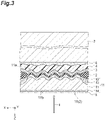
- FIGS. 3 and 4 illustrate a constitution of one pixel P illustrated in FIG. 2 .
- the back-illuminated solid-state imaging element 2 in the imaging unit 10 has a semiconductor layer 11, an insulating layer 12, a plurality of charge transfer electrodes 13 (a generic name of a plurality of charge transfer electrodes 131 and a plurality of charge transfer electrodes 132), a protective layer 14, and an anti-reflective layer 15.
- the semiconductor layer 11 has a front surface 11a and a back surface 11b.
- the front surface 11a is an irregular surface
- the back surface 11b is a flat surface.
- the semiconductor layer 11 includes a p-type semiconductor region (first conduction-type semiconductor region) 111, a plurality of n-type semiconductor regions (second conduction-type semiconductor regions) 112, a plurality of isolation regions 113, and an accumulation region 114.
- the semiconductor layer 11 is a layer formed of silicon.
- the p-type semiconductor region 111 spreads throughout the imaging unit 10 in its entirety.
- the plurality of n-type semiconductor regions 112 are positioned on the front surface 11a side with respect to the p-type semiconductor region 111 and are formed along the front surface 11a which is an irregular surface.
- Each of the n-type semiconductor regions 112 extends in the Y direction for each of the CCD channels C (refer to FIG. 2 ).
- Each of the n-type semiconductor regions 112 forms a p-n junction with the p-type semiconductor region 111.
- the imaging unit 10 is constituted as an embedded channel-type CCD.
- the plurality of isolation regions 113 are positioned on the front surface 11a side with respect to the p-type semiconductor region 111 and are formed along the front surface 11a which is an irregular surface. Each of the isolation regions 113 extends in the Y direction between the n-type semiconductor regions 112 adjacent to each other in the X direction.
- the accumulation region 114 is positioned on the back surface 11b side with respect to the p-type semiconductor region 111 and is formed along the back surface 11b which is a flat surface.
- each of the isolation regions 113 and the accumulation region 114 is a region formed of silicon having a higher p-type impurities concentration than the p-type semiconductor region 111.
- the insulating layer 12 is formed on the front surface 11a of the semiconductor layer 11 such that the plurality of n-type semiconductor regions 112 and the plurality of isolation regions 113 are covered.
- the insulating layer 12 is a layer formed of silicon oxide.
- the plurality of charge transfer electrodes 13 are formed on the insulating layer 12 (more specifically, on a front surface of the insulating layer 12 on a side opposite to the semiconductor layer 11).
- both end portions of the charge transfer electrodes 132 in the Y direction are bent such that they are mounted on end portions of the charge transfer electrodes 131 adjacent to each other in the Y direction via the insulating layer 12.
- each of the charge transfer electrodes 13 is an electrode formed of polysilicon.
- a part 112b other than a part 112a facing each of the charge transfer electrodes 131 has a lower n-type impurities concentration than the part 112a.
- the protective layer 14 is formed to cover the insulating layer 12 and the plurality of charge transfer electrodes 13.
- the protective layer 14 is a layer formed of boro-phospho silicate glass (BPSG).
- the support substrate 3 is attached to a part on the protective layer 14 (more specifically, on a front surface of the protective layer 14 on a side opposite to the semiconductor layer 11) using an adhesive 16.
- the anti-reflective layer 15 is formed on the back surface 11b of the semiconductor layer 11 such that the accumulation region 114 is covered.
- the anti-reflective layer 15 is a dielectric multilayer.
- a p-type semiconductor layer 110 having a front surface 110a and a back surface 11b is prepared (first step). Subsequently, for example, by a sputtering method, for example, a mask 50 formed of silicon nitride is formed on the front surface 110a of the semiconductor layer 110. Subsequently, as illustrated in (b) of FIG. 5 , for example, a plurality of openings 51 which are regularly arrayed are formed in the mask 50 through patterning using a photoresist, and parts corresponding to the respective openings 51 on the front surface 110a of the semiconductor layer 110 are exposed. Subsequently, as illustrated in (c) of FIG.
- a first asperity region 110A is formed on the front surface 110a of the semiconductor layer 110 by selectively etching the front surface 110a of the semiconductor layer 110 (that is, by etching the parts corresponding to the respective openings 51 on the front surface 110a of the semiconductor layer 110) (second step). Subsequently, as illustrated in (a) of FIG. 6 , for example, the mask 50 is removed from the front surface 110a of the semiconductor layer 110 through etching using a high temperature phosphoric acid.
- the first asperity region 110A is constituted by a plurality of recessed portions formed in such a manner (a plurality of recessed portions which are regularly arrayed).
- distances between the recessed portions adjacent to each other are approximately 800 nm, and a depth of each of the recessed portions is approximately 120 nm.
- a second asperity region 110B is formed on the front surface 110a of the semiconductor layer 110 by smoothening asperities of the first asperity region 110A through thermal oxidation and etching (third step). More specifically, asperities of the first asperity region 110A are smoothened by forming an oxidation region along the first asperity region 110A through thermal oxidation and removing the oxidation region through etching (for example, wet etching using a fluoric acid or the like).
- Smoothening asperities of the first asperity region 110A denotes smoothening corner portions (for example, rounding corner portions, such as R-chamfering) formed in at least one of apex portions of projecting portions and bottom portions of recessed portions in the asperities.
- smoothening corner portions for example, rounding corner portions, such as R-chamfering
- inclination of a tangential line at each point on the second asperity region 110B continuously changes.
- distances between the recessed portions adjacent to each other are approximately 800 nm, and a depth of each of the recessed portions is approximately 100 nm.
- a mask 60 formed of an inorganic material is formed on the front surface 110a of the semiconductor layer 110.
- the plurality of isolation regions 113 are formed in the semiconductor layer 110 through ion implantation or diffusion of p-type impurities, and for example, an insulating layer 121 (a part of the insulating layer 12) is formed in the semiconductor layer 110 through thermal oxidation. Formation of the plurality of isolation regions 113 through ion implantation or diffusion of the p-type impurities can be performed after formation of the insulating layer 121 through thermal oxidation.
- the mask 60 is removed from the front surface 110a of the semiconductor layer 110, and for example, the insulating layer 12 is formed along the second asperity region 110B through thermal oxidation (fourth step).
- the plurality of n-type semiconductor regions 112 are formed in the semiconductor layer 110 along the second asperity region 110B through ion implantation of n-type impurities.
- the plurality of charge transfer electrodes 13 are formed on the insulating layer 12, and the protective layer 14 is formed such that the insulating layer 12 and the plurality of charge transfer electrodes 13 are covered.
- the support substrate 3 is attached to a part on the protective layer 14 using the adhesive 16. Namely, the support substrate 3 is attached to parts on the plurality of charge transfer electrodes 13 (fifth step).
- the semiconductor layer 110 is thinned by polishing a back surface 110b of the semiconductor layer 110, for example, through chemical polishing or the like in a state in which the support substrate 3 is attached thereto (sixth step). Subsequently, as illustrated in (b) of FIG.
- the accumulation region 114 is formed in the semiconductor layer 11 along the polished back surface 110b of the semiconductor layer 110 (that is, the back surface 11b of the semiconductor layer 11) through ion implantation of the p-type impurities (seventh step). Subsequently, as illustrated in (c) of FIG. 8 , the anti-reflective layer 15 is formed on the back surface 11b of the semiconductor layer 11 such that the accumulation region 114 is covered.
- the first asperity region 110A is formed on the front surface 110a of the semiconductor layer 110 by selectively etching the front surface 110a of the semiconductor layer 110. Accordingly, in consideration of a shape of the second asperity region 110B capable of curbing occurrence of an etalon phenomenon, the first asperity region 110A having a desired shape can be easily and reliably formed. Moreover, the second asperity region 110B is formed on the front surface 110a of the semiconductor layer 110 by smoothening asperities of the first asperity region 110A.
- a manufactured back-illuminated solid-state imaging device 1 it is possible to curb concentration of an electric field in the apex portions of the projecting portions and the bottom portions of the recessed portions in the second asperity region 110B, and therefore transfer of charges is allowed to sufficiently function.
- the method for manufacturing the back-illuminated solid-state imaging device 1 it is possible to easily and reliably manufacture a back-illuminated solid-state imaging device 1 capable of curbing occurrence of an etalon phenomenon.
- the n-type semiconductor regions 112 are formed in the semiconductor layer 110 along the second asperity region 110B. Accordingly, an embedded channel-type CCD can be constituted.
- asperities of the first asperity region 110A are smoothened through thermal oxidation and etching. Accordingly, asperities of the first asperity region 110A can be easily and reliably smoothened.
- the support substrate 3 is attached to parts on the plurality of charge transfer electrodes 13, the semiconductor layer 110 is thinned by polishing the back surface 110b of the semiconductor layer 110 in this state, and the accumulation region 114 is formed in the semiconductor layer 11 along the polished back surface 110b of the semiconductor layer 110 (that is, the back surface 11b of the semiconductor layer 11). Accordingly, in a manufactured back-illuminated solid-state imaging device 1, generation of dark currents due to a defect which has occurred in the back surface 11b of the semiconductor layer 11 can be curbed through polishing.
- the present disclosure is not limited to the embodiment described above.
- the recessed portions having inner surfaces not depending on crystal orientation of the semiconductor layer 110 are formed in the parts corresponding to the respective openings 51 on the front surface 110a of the semiconductor layer 110.
- the first asperity region 110A may be formed on the front surface 110a of the semiconductor layer 110.
- corner portions are formed in the apex portions of the projecting portions in the asperities of the first asperity region 110A.
- the second asperity region 110B is formed on the front surface 110a of the semiconductor layer 110 by smoothening asperities of the first asperity region 110A.
- Etching for forming the first asperity region 110A on the front surface 110a of the semiconductor layer 110 may be either anisotropic etching or isotropic etching and may be either wet etching or dry etching. However, in the case of dry etching, in order to curb occurrence of a defect on the front surface, it is preferable to adopt chemical dry etching.
- the second asperity region 110B may be formed on the front surface 110a of the semiconductor layer 110 by smoothening asperities of the first asperity region 110A through isotropic etching.
- asperities of the first asperity region 110A can be easily and reliably smoothened.
- Etching for forming the second asperity region 110B on the front surface 110a of the semiconductor layer 110 may be either wet etching or dry etching.
- isotropic etching there is a need to adopt isotropic etching.
- the imaging unit 10 may be constituted as a surface channel-type CCD.
- asperities may be constituted by a plurality of dot-shaped recessed portions or may be constituted by a plurality of projection-shaped projecting portions.
- asperities may be constituted by a plurality of groove-shaped recessed portions or may be constituted by a plurality of wall-shaped projecting portions.
- each of the recessed portions or each of the projecting portions extend in a direction in which a plurality of charge transfer electrodes 13 are arrayed.
- asperities may be formed in a regular pattern, or asperities may be formed in an irregular pattern.
- a plurality of openings 51 which are irregularly disposed may be formed in the mask 50 for forming the first asperity region 110A.
- the back-illuminated solid-state imaging element 2 and the support substrate 3 may be joined to each other (for example, direct bonding) such that an electrode pad of the back-illuminated solid-state imaging element 2 and an electrode pad of the support substrate 3 are electrically connected to each other.
- the conduction types of the p-type and the n-type may be the opposite of that described above. Namely, the first conduction type may be the n-type, and the second conduction type may be the p-type.
- 1 back-illuminated solid-state imaging device
- 3 support substrate
- 110A first asperity region
- 110B second asperity region
- 112 n-type semiconductor region (semiconductor region of second conduction type)
- 114 accumulation region.
Landscapes
- Solid State Image Pick-Up Elements (AREA)
- Transforming Light Signals Into Electric Signals (AREA)
- Light Receiving Elements (AREA)
Applications Claiming Priority (2)
| Application Number | Priority Date | Filing Date | Title |
|---|---|---|---|
| JP2020007338A JP7502866B2 (ja) | 2020-01-21 | 2020-01-21 | 裏面入射型固体撮像装置の製造方法 |
| PCT/JP2021/001711 WO2021149686A1 (ja) | 2020-01-21 | 2021-01-19 | 裏面入射型固体撮像装置の製造方法 |
Publications (2)
| Publication Number | Publication Date |
|---|---|
| EP4089736A1 true EP4089736A1 (de) | 2022-11-16 |
| EP4089736A4 EP4089736A4 (de) | 2024-02-21 |
Family
ID=76992973
Family Applications (1)
| Application Number | Title | Priority Date | Filing Date |
|---|---|---|---|
| EP21744437.1A Pending EP4089736A4 (de) | 2020-01-21 | 2021-01-19 | Verfahren zur herstellung einer back-thinned-festkörperbildgebungsvorrichtung |
Country Status (6)
| Country | Link |
|---|---|
| US (1) | US20230045038A1 (de) |
| EP (1) | EP4089736A4 (de) |
| JP (1) | JP7502866B2 (de) |
| KR (1) | KR20220129011A (de) |
| CN (1) | CN114930539B (de) |
| WO (1) | WO2021149686A1 (de) |
Family Cites Families (17)
| Publication number | Priority date | Publication date | Assignee | Title |
|---|---|---|---|---|
| JPH0621016Y2 (ja) * | 1988-02-10 | 1994-06-01 | 横河電機株式会社 | 導電率計 |
| JPH0621016A (ja) * | 1992-07-01 | 1994-01-28 | Seiko Epson Corp | 半導体装置の製造方法 |
| KR20020044364A (ko) * | 2000-12-05 | 2002-06-15 | 박종섭 | 반도체 소자의 커패시터 제조 방법 |
| JP4442157B2 (ja) * | 2003-08-20 | 2010-03-31 | ソニー株式会社 | 光電変換装置及び固体撮像装置 |
| JP2005101864A (ja) * | 2003-09-24 | 2005-04-14 | Sony Corp | 固体撮像素子の駆動方法、固体撮像装置 |
| JP2006229112A (ja) * | 2005-02-21 | 2006-08-31 | Casio Comput Co Ltd | 半導体装置およびその製造方法 |
| US7982177B2 (en) * | 2008-01-31 | 2011-07-19 | Omnivision Technologies, Inc. | Frontside illuminated image sensor comprising a complex-shaped reflector |
| JP2009272596A (ja) * | 2008-04-09 | 2009-11-19 | Sony Corp | 固体撮像装置とその製造方法、及び電子機器 |
| JP5185206B2 (ja) * | 2009-02-24 | 2013-04-17 | 浜松ホトニクス株式会社 | 半導体光検出素子 |
| JP5185205B2 (ja) * | 2009-02-24 | 2013-04-17 | 浜松ホトニクス株式会社 | 半導体光検出素子 |
| JP5394791B2 (ja) * | 2009-03-27 | 2014-01-22 | 浜松ホトニクス株式会社 | 裏面入射型固体撮像素子 |
| JP2010283223A (ja) * | 2009-06-05 | 2010-12-16 | Hamamatsu Photonics Kk | 半導体光検出素子及び半導体光検出素子の製造方法 |
| JP2012049289A (ja) * | 2010-08-26 | 2012-03-08 | Sony Corp | 固体撮像装置とその製造方法、並びに電子機器 |
| JP2012199417A (ja) * | 2011-03-22 | 2012-10-18 | Kyushu Institute Of Technology | 高アスペクト比のトレンチ構造を有する半導体デバイスの製造方法 |
| JP2015076569A (ja) * | 2013-10-11 | 2015-04-20 | ソニー株式会社 | 撮像装置およびその製造方法ならびに電子機器 |
| JP2017126642A (ja) * | 2016-01-13 | 2017-07-20 | 浜松ホトニクス株式会社 | 裏面入射型固体撮像素子及びその製造方法 |
| CN111033744B (zh) * | 2017-10-31 | 2023-04-21 | 松下知识产权经营株式会社 | 结构体及其制造方法 |
-
2020
- 2020-01-21 JP JP2020007338A patent/JP7502866B2/ja active Active
-
2021
- 2021-01-19 CN CN202180008815.2A patent/CN114930539B/zh active Active
- 2021-01-19 EP EP21744437.1A patent/EP4089736A4/de active Pending
- 2021-01-19 WO PCT/JP2021/001711 patent/WO2021149686A1/ja not_active Ceased
- 2021-01-19 US US17/792,799 patent/US20230045038A1/en active Pending
- 2021-01-19 KR KR1020227026813A patent/KR20220129011A/ko not_active Ceased
Also Published As
| Publication number | Publication date |
|---|---|
| KR20220129011A (ko) | 2022-09-22 |
| CN114930539B (zh) | 2025-08-26 |
| EP4089736A4 (de) | 2024-02-21 |
| JP2021114572A (ja) | 2021-08-05 |
| WO2021149686A1 (ja) | 2021-07-29 |
| CN114930539A (zh) | 2022-08-19 |
| US20230045038A1 (en) | 2023-02-09 |
| JP7502866B2 (ja) | 2024-06-19 |
Similar Documents
| Publication | Publication Date | Title |
|---|---|---|
| EP2413362B1 (de) | Rückseitig beleuchtete festkörperbildaufnahmevorrichtung | |
| EP2863437B1 (de) | Festkörperbilderfassungsvorrichtung | |
| CN1638134B (zh) | 固态图像拾取装置 | |
| US20220262829A1 (en) | Semiconductor device | |
| KR102109952B1 (ko) | 이미지 센서 및 이의 형성 방법 | |
| US7598553B2 (en) | CMOS image sensor and method of manufacturing thereof | |
| JP3225939B2 (ja) | 固体撮像装置及びその製造方法 | |
| KR100538069B1 (ko) | 암신호 감소를 위한 이미지센서의 소자분리 방법 | |
| JP4863214B2 (ja) | 薄膜化シリコンからなる電子チップの製造方法 | |
| EP4089736A1 (de) | Verfahren zur herstellung einer back-thinned-festkörperbildgebungsvorrichtung | |
| US7541631B2 (en) | Solid-state imaging device | |
| JP4194295B2 (ja) | 固体撮像素子の製造方法 | |
| CN115224064B (zh) | 背照式图像传感器及其制作方法 | |
| CN117276294A (zh) | 背照式图像传感器及其形成方法 | |
| CN114156300A (zh) | 背照式图像传感器及其形成方法 | |
| KR20220164329A (ko) | 이미지 센서 | |
| KR100855960B1 (ko) | 기판 스트레스를 억제할 수 있는 cmos 이미지 소자 및그 제조방법 | |
| KR100752654B1 (ko) | 반도체 기판의 후면에 전원전압을 인가하는 이미지 센서 및이미지 센서의 제조 방법 | |
| JP2011151139A (ja) | 固体撮像素子の製造方法および固体撮像素子 | |
| JP4715110B2 (ja) | 固体撮像素子の製造方法 | |
| JP2006294654A (ja) | 固体撮像装置及びその製造方法 | |
| CN118723921A (zh) | 半导体结构的形成方法 | |
| CN118380452A (zh) | 图像传感器及其制造方法 | |
| JP2009054700A (ja) | 固体撮像素子の製造方法および固体撮像素子 | |
| CN115706119A (zh) | 背照式影像传感器及其制造方法 |
Legal Events
| Date | Code | Title | Description |
|---|---|---|---|
| STAA | Information on the status of an ep patent application or granted ep patent |
Free format text: STATUS: THE INTERNATIONAL PUBLICATION HAS BEEN MADE |
|
| PUAI | Public reference made under article 153(3) epc to a published international application that has entered the european phase |
Free format text: ORIGINAL CODE: 0009012 |
|
| STAA | Information on the status of an ep patent application or granted ep patent |
Free format text: STATUS: REQUEST FOR EXAMINATION WAS MADE |
|
| 17P | Request for examination filed |
Effective date: 20220809 |
|
| AK | Designated contracting states |
Kind code of ref document: A1 Designated state(s): AL AT BE BG CH CY CZ DE DK EE ES FI FR GB GR HR HU IE IS IT LI LT LU LV MC MK MT NL NO PL PT RO RS SE SI SK SM TR |
|
| DAV | Request for validation of the european patent (deleted) | ||
| DAX | Request for extension of the european patent (deleted) | ||
| A4 | Supplementary search report drawn up and despatched |
Effective date: 20240119 |
|
| RIC1 | Information provided on ipc code assigned before grant |
Ipc: H01L 27/146 20060101ALI20240115BHEP Ipc: H01L 27/148 20060101AFI20240115BHEP |