EP4080274B1 - Herstellungsverfahren für anzeigemodul, anzeigemodul und elektronisches gerät - Google Patents
Herstellungsverfahren für anzeigemodul, anzeigemodul und elektronisches gerät Download PDFInfo
- Publication number
- EP4080274B1 EP4080274B1 EP20901500.7A EP20901500A EP4080274B1 EP 4080274 B1 EP4080274 B1 EP 4080274B1 EP 20901500 A EP20901500 A EP 20901500A EP 4080274 B1 EP4080274 B1 EP 4080274B1
- Authority
- EP
- European Patent Office
- Prior art keywords
- substrate
- away
- partial structure
- display module
- light
- Prior art date
- Legal status (The legal status is an assumption and is not a legal conclusion. Google has not performed a legal analysis and makes no representation as to the accuracy of the status listed.)
- Active
Links
Images
Classifications
-
- G—PHYSICS
- G02—OPTICS
- G02F—OPTICAL DEVICES OR ARRANGEMENTS FOR THE CONTROL OF LIGHT BY MODIFICATION OF THE OPTICAL PROPERTIES OF THE MEDIA OF THE ELEMENTS INVOLVED THEREIN; NON-LINEAR OPTICS; FREQUENCY-CHANGING OF LIGHT; OPTICAL LOGIC ELEMENTS; OPTICAL ANALOGUE/DIGITAL CONVERTERS
- G02F1/00—Devices or arrangements for the control of the intensity, colour, phase, polarisation or direction of light arriving from an independent light source, e.g. switching, gating or modulating; Non-linear optics
- G02F1/01—Devices or arrangements for the control of the intensity, colour, phase, polarisation or direction of light arriving from an independent light source, e.g. switching, gating or modulating; Non-linear optics for the control of the intensity, phase, polarisation or colour
- G02F1/13—Devices or arrangements for the control of the intensity, colour, phase, polarisation or direction of light arriving from an independent light source, e.g. switching, gating or modulating; Non-linear optics for the control of the intensity, phase, polarisation or colour based on liquid crystals, e.g. single liquid crystal display cells
- G02F1/133—Constructional arrangements; Operation of liquid crystal cells; Circuit arrangements
- G02F1/1333—Constructional arrangements; Manufacturing methods
- G02F1/133302—Rigid substrates, e.g. inorganic substrates
-
- G—PHYSICS
- G02—OPTICS
- G02F—OPTICAL DEVICES OR ARRANGEMENTS FOR THE CONTROL OF LIGHT BY MODIFICATION OF THE OPTICAL PROPERTIES OF THE MEDIA OF THE ELEMENTS INVOLVED THEREIN; NON-LINEAR OPTICS; FREQUENCY-CHANGING OF LIGHT; OPTICAL LOGIC ELEMENTS; OPTICAL ANALOGUE/DIGITAL CONVERTERS
- G02F1/00—Devices or arrangements for the control of the intensity, colour, phase, polarisation or direction of light arriving from an independent light source, e.g. switching, gating or modulating; Non-linear optics
- G02F1/01—Devices or arrangements for the control of the intensity, colour, phase, polarisation or direction of light arriving from an independent light source, e.g. switching, gating or modulating; Non-linear optics for the control of the intensity, phase, polarisation or colour
- G02F1/13—Devices or arrangements for the control of the intensity, colour, phase, polarisation or direction of light arriving from an independent light source, e.g. switching, gating or modulating; Non-linear optics for the control of the intensity, phase, polarisation or colour based on liquid crystals, e.g. single liquid crystal display cells
- G02F1/133—Constructional arrangements; Operation of liquid crystal cells; Circuit arrangements
- G02F1/1333—Constructional arrangements; Manufacturing methods
-
- G—PHYSICS
- G02—OPTICS
- G02F—OPTICAL DEVICES OR ARRANGEMENTS FOR THE CONTROL OF LIGHT BY MODIFICATION OF THE OPTICAL PROPERTIES OF THE MEDIA OF THE ELEMENTS INVOLVED THEREIN; NON-LINEAR OPTICS; FREQUENCY-CHANGING OF LIGHT; OPTICAL LOGIC ELEMENTS; OPTICAL ANALOGUE/DIGITAL CONVERTERS
- G02F1/00—Devices or arrangements for the control of the intensity, colour, phase, polarisation or direction of light arriving from an independent light source, e.g. switching, gating or modulating; Non-linear optics
- G02F1/01—Devices or arrangements for the control of the intensity, colour, phase, polarisation or direction of light arriving from an independent light source, e.g. switching, gating or modulating; Non-linear optics for the control of the intensity, phase, polarisation or colour
- G02F1/13—Devices or arrangements for the control of the intensity, colour, phase, polarisation or direction of light arriving from an independent light source, e.g. switching, gating or modulating; Non-linear optics for the control of the intensity, phase, polarisation or colour based on liquid crystals, e.g. single liquid crystal display cells
- G02F1/133—Constructional arrangements; Operation of liquid crystal cells; Circuit arrangements
- G02F1/13306—Circuit arrangements or driving methods for the control of single liquid crystal cells
- G02F1/13312—Circuits comprising photodetectors for purposes other than feedback
Definitions
- the present disclosure relates to the technical field of display, and in particular, to a preparation method of a display module, the display module, and an electronic device.
- a light-transmitting area may be arranged on the display module of the electronic device, and the camera and other optical devices are arranged facing towards the light-transmitting area, so that the functions of the optical devices are realized.
- the display module may include a first substrate and a second substrate which are stacked.
- other structures are not arranged between parts of the first substrate and the second substrate located in the light-transmitting area as far as possible.
- the parts of the first substrate and the second substrate located in the light-transmitting area are prone to concave deformation, so that the optical performance of the light-transmitting area is affected, resulting in poor performance of the optical devices.
- US20080023438A1 discloses a method of manufacturing a liquid crystal display apparatus, which includes forming at least one assembly for forming a plurality of finished liquid crystal display apparatuses, by opposing two glass substrates to have a space there between and sealing a periphery of the space between the two glass substrates by an outer peripheral seal member.
- Outer surfaces of the two glass substrates are etched by soaking the assembly in an etching solution within an etching bath while maintaining a temperature and a concentration of the etching solution within the etching bath at a substantially constant temperature and at a substantially constant concentration.
- the etched outer surfaces of the glass substrates are flattened by polishing the outer surfaces of the glass substrates.
- CN109407375A discloses a display panel, a making method thereof, a display screen assembly and electronic equipment.
- the display panel comprises a light-pervious area located in an effective display area of the display panel, and used for providing a light path penetrating through the display panel in the thickness direction for a non-display surface of the display panel, and the non-display face of the display panel is provided with at least a transparent conducting layer covering the light-pervious area.
- a conductive path is provided for back static electricity, the static electricity is effectively dispersed and guided away, and a circuit in the display panel is protected.
- the CN110275340A provides a liquid crystal display device for an in-screen recognition scheme.
- the liquid crystal display device for the in-screen recognition scheme includes a liquid crystal module, a backlight module, an in-screen sensor, and a micro LED module.
- the micro LED module defines a micro LED operable region.
- the micro LED operable region is seamlessly coupled to the liquid crystal module operable region of the liquid crystal module, thereby avoiding visual display interruption and discontinuous boundaries to achieve complete full-screen design.
- the CN110426885A provides a display panel, a production method and a display device.
- the display panel comprises a first substrate, a second substrate, a liquid crystal layer and a camera-shooting component, wherein the liquid crystal layer is arranged between the first substrate and the second substrate, the camera-shooting component is arranged at the side, away from the first substrate, of the second substrate, a color filtering layer is arranged at the side, close to the second substrate, of the first substrate, a light-transmitting part is arranged at the position, corresponding to the camera-shooting component, of the color filtering layer, and a thin film transistor layer is arranged at the side, close to the first substrate, of the second substrate.
- CN110579911A relates to a display panel, a display device and a mobile terminal.
- the display panel is defined to have a display area and a camera area.
- a closed accommodating space is formed by a first substrate layer, a second substrate layer and frame glue, and the accommodating space is filled with a liquid crystal material to form a first liquid crystal layer, so that the phenomenon of gravity or non-uniform box thickness caused by liquid crystal box thickness height difference between the first liquid crystal layer and a second liquid crystal layer is avoided.
- the claimed invention provides a preparation method of a display module as defined in claim 1, a display module as defined in claim 7, and an electronic device as defined in claim 8, so as to solve the problem of poor performance of the optical devices.
- a preparation method of a display module includes amongst others:
- a display module is prepared by the preparation method, the display module has amongst other features a light-transmitting area, a surface of one side of the first substrate away from the second substrate is a plane, and a surface of one side of the second substrate away from the first substrate is a plane.
- An electronic device includes the display module, and further includes an optical device, wherein the optical device and the second substrate are located on two sides of the first substrate respectively, and the light-transmitting area and the optical device are arranged oppositely.
- the technical solutions used by the present disclosure can achieve the following beneficial effects: in the preparation method of the present disclosure, after the first substrate and the second substrate are bonded, the partial structure of one side of the first substrate away from the second substrate can be removed, so that the surface of one side of the first substrate away from the second substrate is a plane; meanwhile, the partial structure of one side of the second substrate away from the first substrate is removed, so that the surface of one side of the second substrate away from the first substrate is a plane; therefore, by the preparation method, the concave deformation of the parts of the first substrate and the second substrate located in the light-transmitting area can be relieved, so that the optical performance of the light-transmitting area and the performance of the optical device are improved.
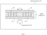
- A-light-transmitting area 110-first substrate, 120-second substrate, 130-liquid crystal layer, 140-supporting column.
- the embodiments of the present disclosure disclose a preparation method of a display module.
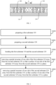
- the preparation method is used to prepare the display module shown in FIG. 1 .
- the display module may be applied to an electronic device with an optical device.
- the display module has a light-transmitting area A, the light-transmitting area A has high light transmittance, and the optical device of the electronic device may be arranged towards the light-transmitting area A, so that light in the external environment may enter the optical device through the light-transmitting area A, or light emitted by the optical device may enter the external environment through the light-transmitting area A.
- a shape of the light-transmitting area A may be designed according to the structure of the optical device.
- the light-transmitting area A may be a circular area
- the other area of the display module may be mainly used for displaying, and this area may surround the light-transmitting area A.
- the first substrate 110 and the second substrate 120 are stacked.
- the first substrate 110 and the second substrate 120 may adopt glass plates with high light transmittance.
- a thin film transistor is arranged on one surface of the first substrate 110 facing towards the second substrate 120.
- a plurality of thin film transistors may be provided, the thin film transistors are arranged on the first substrate 110 in an array, and the thin film transistors may drive the display module.
- S400 removing a partial structure of one side of the first substrate 110 away from the second substrate 120, so that a surface of one side of the first substrate 110 away from the second substrate 120 is a plane.
- S500 removing a partial structure of the second substrate 120 away from the first substrate 110, so that a surface of one side of the second substrate 120 away from the first substrate 110 is plane.
- the preparation method disclosed by the embodiments of the present disclosure after the first substrate 110 and the second substrate 120 are bonded, the partial structure of one side of the first substrate 110 away from the second substrate 120 is removed, so that the surface of one side of the first substrate 110 away from the second substrate 120 is a plane; meanwhile, the partial structure of one side of the second substrate 120 away from the first substrate 110 is removed, so that the surface of one side of the second substrate 120 away from the first substrate 110 is a plane; therefore, by the preparation method, the concave deformation of the parts of the first substrate 110 and the second substrate 120 located in the light-transmitting area A is relieved, so that the optical performance of the light-transmitting area A and the performance of the optical device are improved.
- the step S400 of removing the partial structure of one side of the first substrate 110 away from the second substrate 120 includes: removing the partial structure of one side of the first substrate 110 away from the second substrate 120 by a polishing process.
- the processing precision of the polishing process is relatively high, so after the partial structure of the first substrate 110 is removed by the polishing process, the flatness of the surface of one side of the first substrate 110 away from the second substrate 120 is further improved, and the optical performance of the light-transmitting area A is better.
- the partial structure of one side of the first substrate 110 away from the second substrate 120 may also be removed by a cutting process, which will not be limited in the embodiments of the present disclosure.
- the method further includes: performing etching operation on the first substrate 110.
- the processing precision of the polishing process is high.
- the thickness of a to-be-removed part on the first substrate 110 is large, the cost of the polishing process will be increased, resulting in a relatively high forming process of the display module.
- the processing precision of the etching operation is relatively lower, so the operation cost is lower and the partial structure of the first substrate 110 can be removed. Therefore, the etching operation is performed before the polishing process, and the thickness of the part of the first substrate 110 removed by the polishing process can be effectively reduced, so that the polishing process can be performed at a lower cost.
- the step S500 of removing the partial structure of one side of the second substrate 120 away from the first substrate 110 includes: removing the partial structure of one side of the second substrate 120 away from the first substrate 110 by a polishing process.
- the processing precision of the polishing process is relatively high, so after the partial structure of the second substrate 120 is removed by the polishing process, the flatness of the surface of one side of the second substrate 120 away from the first substrate 110 is further improved, and the optical performance of the light-transmitting area A is better.
- the partial structure of one side of the second substrate 120 away from the first substrate 110 may also be removed by a cutting process, which will not be limited in the embodiments of the present disclosure.
- the method further includes: performing etching operation on the second substrate 120.
- the processing precision of the polishing process is high.
- the thickness of a to-be-removed part on the second substrate 120 is large, the cost of the polishing process will be increased, resulting in a relatively high forming process of the display module.
- the processing precision of the etching operation is relatively lower, so the operation cost is lower and the partial structure of the second substrate 120 can be removed. Therefore, the etching operation is performed before the polishing process, and the thickness of the part of the second substrate 120 removed by the polishing process can be effectively reduced, so that the polishing process can be performed at a lower cost.
- the influence on the optical performance of the light-transmitting area A by the concave deformation of the first substrate 110 and the second substrate 120 can be eliminated.
- the concave deformation of the first substrate 110 and the second substrate 120 may - in a case not according to the claimed invention - not be eliminated.
- the thickness of the removed parts of the first substrate 110 and the second substrate 120 is too large, the structural strength of the first substrate 110 and the second substrate 120 is too low, which easily leads to low structural strength of the display module.
- the thickness of the removed partial structure is 5 - 20 ⁇ m, so that the thickness of the removed part of the first substrate 110 is moderate, the concave deformation of the first substrate 110 is eliminated well, and the structural strength of the first substrate 110 can be ensured.
- the thickness of the removed part of the second substrate 120 may also be optimized:
- the embodiments of the claimed invention further disclose display module 100.
- the display module 100 is prepared by the preparation method provided by any of the embodiments.
- the display module 100 has a light-transmitting area A, the first substrate 110 and the second substrate 120 are stacked, the surface of one side of the first substrate 110 away from the second substrate 120 is a plane, and the surface of one side of the second substrate 120 away from the first substrate 110 is a plane, so that the concave deformation of the parts of the first substrate 110 and the second substrate 120 located in the light-transmitting area A is relieved, and the optical performance of the light-transmitting area A and the performance of the optical device are improved.
- the display module is a liquid crystal display module.
- the display module further includes a liquid crystal layer 130, and the liquid crystal layer 130 is arranged between the first substrate 110 and the second substrate 120.
- the display module may also be an organic light-emitting display module.
- the display module further includes an organic light-emitting layer.
- the organic light-emitting layer is arranged between the first substrate 110 and the second substrate 120.
- the first substrate 110, the second substrate 120 and the liquid crystal layer 130 have the same refractive index.
- the first substrate 110, the second substrate 120 and the liquid crystal layer 130 may also be regarded as an integral structure, so that during light propagation, there will be basically no excessive directional changes. Therefore, this arrangement can improve the optical performance of the light-transmitting area A, and the performance of the optical device is better.
- the refractive indexes of the first substrate 110, the second substrate 120 and the liquid crystal layer 130 may be set to about 1.5.
- the display module may further include a plurality of supporting columns 140, each supporting column 140 is arranged between the first substrate 110 and the second substrate 120, and the supporting columns 140 are arranged at intervals. Each supporting column 140 may apply a supporting force to the first substrate 110 and the second substrate 120, so that the substrate 110 and the second substrate 120 are not liable to deform
- the embodiments of the claimed invention further discloses an electronic device 300.
- the electronic device 300 includes the display module 100 provided by any of the above embodiments, and further includes an optical device 200, wherein the optical device 200 and the second substrate 120 are located on two sides of the first substrate 110 respectively, and the light-transmitting area A of the display module and the optical device are arranged oppositely.
- the optical device includes at least one of a fingerprint module, a camera, a sensor or a light supplement lamp, so that the corresponding fingerprint recognition, shooting, data detection and light supplement functions can be realized; and these optical devices may not occupy the display area of the electronic device, so that the screen-to-body ratio of the electronic device is higher.
- the optical device may further include other devices with light receiving function or light emitting function, which will not be limited in the embodiments of the present disclosure.
- the electronic device disclosed in the embodiments of the present disclosure may be a smart phone, a tablet computer, an e-book reader, or a wearable device.
- the electronic device may also be other devices, which is not limited in the embodiments of the present disclosure.
Landscapes
- Physics & Mathematics (AREA)
- Nonlinear Science (AREA)
- Chemical & Material Sciences (AREA)
- Mathematical Physics (AREA)
- Crystallography & Structural Chemistry (AREA)
- General Physics & Mathematics (AREA)
- Optics & Photonics (AREA)
- Inorganic Chemistry (AREA)
- Devices For Indicating Variable Information By Combining Individual Elements (AREA)
- Electroluminescent Light Sources (AREA)
Claims (9)
- Herstellungsverfahren für ein Anzeigemodul, wobei das Anzeigemodul eine Lichtübertragungsfläche (A) umfasst, in deren Richtung eine optische Vorrichtung in einer solchen Weise angeordnet sein kann, dass von der optischen Vorrichtung empfangenes oder emittiertes Licht die Lichtübertragungsfläche durchläuft, wobei das Verfahren umfasst:Herstellen (S100) eines ersten Substrats (110);Herstellen (S200) eines zweiten Substrats (120);Verbinden (S300) des ersten Substrats (110) und des zweiten Substrats (120), wobei die in der Lichtübertragungsfläche (A) befindlichen Teile des ersten und zweiten Substrats konkav sind;Entfernen (S400) einer Teilstruktur einer von dem zweiten Substrat (120) abgewandten Seite des ersten Substrats (110), sodass eine Oberfläche einer von dem zweiten Substrat (120) abgewandten Seite des ersten Substrats (110) eine Ebene ist; undEntfernen (S500) einer Teilstruktur einer von dem ersten Substrat (110) angewandten Seite des zweiten Substrats (120), sodass eine Oberfläche einer von dem ersten Substrat (110) abgewandten Seite des zweiten Substrats (120) eine Ebene ist.
- Herstellungsverfahren nach Anspruch 1, wobei der Schritt des Entfernens einer Teilstruktur einer von dem zweiten Substrat (120) abgewandten Seite des ersten Substrats (110) ferner umfasst:
Entfernen der Teilstruktur einer von dem zweiten Substrat (120) abgewandten Seite des ersten Substrats (110) durch einen Polierprozess. - Herstellungsverfahren nach Anspruch 2, wobei das Verfahren vor dem Entfernen der Teilstruktur einer von dem zweiten Substrat (120) abgewandten Seite des ersten Substrats (110) ferner umfasst:
Durchführen eines Ätzvorgangs auf dem ersten Substrat (110). - Herstellungsverfahren nach Anspruch 1, wobei der Schritt des Entfernens der Teilstruktur einer von dem ersten Substrat (110) abgewandten Seite des zweiten Substrats (120) ferner umfasst:
Entfernen der Teilstruktur einer von dem ersten Substrat (110) abgewandten Seite des zweiten Substrats (120) durch einen Polierprozess. - Herstellungsverfahren nach Anspruch 4, wobei das Verfahren vor dem Entfernen der Teilstruktur einer von dem ersten Substrat (110) abgewandten Seite des zweiten Substrats (120) ferner umfasst:
Durchführen eines Ätzvorgangs auf dem zweiten Substrat (120). - Herstellungsverfahren nach Anspruch 1, wobei im Schritt des Entfernens der Teilstruktur einer von dem zweiten Substrat (120) abgewandten Seite des ersten Substrats (110) eine Dicke der entfernten Teilstruktur 5-20 µm beträgt; und/oder
im Schritt des Entfernens der Teilstruktur einer von dem ersten Substrat (110) abgewandten Seite des zweiten Substrats (120) eine Dicke der entfernten Teilstruktur 5-20 µm beträgt. - Anzeigemodul (100), hergestellt durch das Herstellungsverfahren nach einem der Ansprüche 1-6, wobei eine von dem zweiten Substrat (120) abgewandte Oberfläche einer Seite des ersten Substrats (110) eine Ebene ist und eine von dem ersten Substrat (110) abgewandte Oberfläche einer Seite des zweiten Substrats (120) eine Ebene ist; wobei das Anzeigemodul ferner eine Flüssigkristallschicht (130) umfasst, wobei die Flüssigkristallschicht (130) zwischen dem ersten Substrat (110) und dem zweiten Substrat (120) angeordnet ist; wobei das erste Substrat (110), das zweite Substrat (120) und die Flüssigkristallschicht (130) den gleichen Brechungsindex aufweisen.
- Elektronisches Gerät (300), umfassend das Anzeigemodul (100) nach Anspruch 7 und ferner umfassend eine optische Vorrichtung (200), wobei sich die optische Vorrichtung (200) beziehungsweise das zweite Substrat (120) auf zwei Seiten des ersten Substrats (110) befinden und die Lichtübertragungsfläche (A) und die optische Vorrichtung (200) einander gegenüberliegend angeordnet sind.
- Elektronische Vorrichtung nach Anspruch 8, wobei die optische Vorrichtung mindestens ein Fingerabdruckmodul, eine Kamera, einen Sensor, einen Empfänger und/oder eine Zusatzlichtlampe umfasst.
Applications Claiming Priority (2)
| Application Number | Priority Date | Filing Date | Title |
|---|---|---|---|
| CN201911328934.7A CN111142284A (zh) | 2019-12-20 | 2019-12-20 | 显示模组的制备方法、显示模组及电子设备 |
| PCT/CN2020/137430 WO2021121351A1 (zh) | 2019-12-20 | 2020-12-18 | 显示模组的制备方法、显示模组及电子设备 |
Publications (3)
| Publication Number | Publication Date |
|---|---|
| EP4080274A1 EP4080274A1 (de) | 2022-10-26 |
| EP4080274A4 EP4080274A4 (de) | 2023-06-07 |
| EP4080274B1 true EP4080274B1 (de) | 2025-06-04 |
Family
ID=70519158
Family Applications (1)
| Application Number | Title | Priority Date | Filing Date |
|---|---|---|---|
| EP20901500.7A Active EP4080274B1 (de) | 2019-12-20 | 2020-12-18 | Herstellungsverfahren für anzeigemodul, anzeigemodul und elektronisches gerät |
Country Status (5)
| Country | Link |
|---|---|
| US (1) | US12105366B2 (de) |
| EP (1) | EP4080274B1 (de) |
| CN (1) | CN111142284A (de) |
| ES (1) | ES3035563T3 (de) |
| WO (1) | WO2021121351A1 (de) |
Families Citing this family (2)
| Publication number | Priority date | Publication date | Assignee | Title |
|---|---|---|---|---|
| CN111142284A (zh) | 2019-12-20 | 2020-05-12 | 维沃移动通信有限公司 | 显示模组的制备方法、显示模组及电子设备 |
| CN114994978B (zh) * | 2022-05-18 | 2023-09-26 | 厦门天马微电子有限公司 | 显示模组和显示装置 |
Family Cites Families (26)
| Publication number | Priority date | Publication date | Assignee | Title |
|---|---|---|---|---|
| KR100667790B1 (ko) * | 2005-01-10 | 2007-01-11 | 삼성전자주식회사 | 복굴절 보정용 액정소자 및 이를 구비한 광픽업 및 광기록 및/또는 재생기기 |
| JP2007219403A (ja) * | 2006-02-20 | 2007-08-30 | Nanox Corp | 反射型カラー液晶表示装置及びその製造方法 |
| JP4197018B2 (ja) * | 2006-07-31 | 2008-12-17 | カシオ計算機株式会社 | 液晶表示装置の製造方法 |
| CN101816026A (zh) * | 2007-10-22 | 2010-08-25 | 夏普株式会社 | 显示装置及其制造方法 |
| JPWO2009107453A1 (ja) * | 2008-02-29 | 2011-06-30 | 日本板硝子株式会社 | 表示装置用ガラス基板、液晶表示パネル、並びに液晶表示装置 |
| CN201400130Y (zh) * | 2009-02-27 | 2010-02-10 | 比亚迪股份有限公司 | 防炫后视镜 |
| DE102011089443B4 (de) * | 2011-02-14 | 2016-12-01 | Lg Display Co., Ltd. | Anzeigevorrichtung |
| KR101799937B1 (ko) * | 2011-05-12 | 2017-11-22 | 엘지디스플레이 주식회사 | 경량 박형의 액정표시장치의 제조 방법 |
| CN104460095B (zh) * | 2015-01-05 | 2018-05-08 | 京东方科技集团股份有限公司 | 一种显示面板及其制备方法 |
| CN104678666A (zh) * | 2015-03-19 | 2015-06-03 | 京东方科技集团股份有限公司 | 显示面板及其制备方法 |
| JP2017021201A (ja) * | 2015-07-10 | 2017-01-26 | 株式会社リコー | エレクトロクロミック素子の製造方法 |
| CN105607327B (zh) * | 2016-03-25 | 2018-10-26 | 京东方科技集团股份有限公司 | 液晶显示装置的制作方法 |
| CN107946341B (zh) * | 2017-11-10 | 2020-05-22 | 上海天马微电子有限公司 | 显示装置和显示装置的制造方法 |
| CN107817621B (zh) * | 2017-12-15 | 2021-01-26 | 江西沃格光电股份有限公司 | 平板显示器的修复方法 |
| CN108227257B (zh) * | 2018-02-06 | 2021-01-26 | 京东方科技集团股份有限公司 | 一种减薄装置及减薄方法 |
| CN109164648B (zh) * | 2018-09-30 | 2021-11-19 | 厦门天马微电子有限公司 | 一种显示面板及显示装置 |
| CN109407375B (zh) * | 2018-10-16 | 2021-10-15 | Oppo广东移动通信有限公司 | 一种显示面板及其制作方法、显示屏组件、电子设备 |
| US10866464B2 (en) * | 2019-04-17 | 2020-12-15 | Wuhan China Star Optoelectronics Technology Co., Ltd. | Liquid crystal display panel and electronic device |
| CN110275340A (zh) * | 2019-06-10 | 2019-09-24 | 武汉华星光电技术有限公司 | 用于屏下辨识方案的液晶显示设备 |
| CN110426885B (zh) * | 2019-07-22 | 2020-12-04 | 武汉华星光电半导体显示技术有限公司 | 显示面板及制作方法、显示装置 |
| CN110579911A (zh) * | 2019-08-22 | 2019-12-17 | 武汉华星光电技术有限公司 | 一种显示面板及其显示装置、移动终端 |
| CN110501835B (zh) * | 2019-09-19 | 2022-05-13 | 京东方科技集团股份有限公司 | 一种显示面板、其驱动方法及显示装置 |
| CN110794622B (zh) * | 2019-10-08 | 2021-11-02 | 维沃移动通信有限公司 | 显示模组及电子设备 |
| US11036102B1 (en) * | 2019-12-12 | 2021-06-15 | Wuhan China Star Optoelectronics Technology Co., Ltd. | Liquid crystal display panel |
| CN111142284A (zh) * | 2019-12-20 | 2020-05-12 | 维沃移动通信有限公司 | 显示模组的制备方法、显示模组及电子设备 |
| CN111929936B (zh) * | 2020-08-25 | 2023-05-02 | 上海中航光电子有限公司 | 一种显示面板及显示装置 |
-
2019
- 2019-12-20 CN CN201911328934.7A patent/CN111142284A/zh active Pending
-
2020
- 2020-12-18 WO PCT/CN2020/137430 patent/WO2021121351A1/zh not_active Ceased
- 2020-12-18 ES ES20901500T patent/ES3035563T3/es active Active
- 2020-12-18 EP EP20901500.7A patent/EP4080274B1/de active Active
-
2022
- 2022-06-16 US US17/842,702 patent/US12105366B2/en active Active
Also Published As
| Publication number | Publication date |
|---|---|
| WO2021121351A1 (zh) | 2021-06-24 |
| EP4080274A1 (de) | 2022-10-26 |
| CN111142284A (zh) | 2020-05-12 |
| EP4080274A4 (de) | 2023-06-07 |
| US12105366B2 (en) | 2024-10-01 |
| US20220317503A1 (en) | 2022-10-06 |
| ES3035563T3 (en) | 2025-09-04 |
Similar Documents
| Publication | Publication Date | Title |
|---|---|---|
| CN112133708B (zh) | 一种显示面板、显示装置及显示面板的制作方法 | |
| CN209992775U (zh) | 显示装置 | |
| CN207352324U (zh) | 显示母板及显示面板 | |
| EP4043949B1 (de) | Anzeigemodul und elektronische vorrichtung | |
| US20040141096A1 (en) | Flat display device with touch panel | |
| CN109307962A (zh) | 一种液晶显示面板、液晶显示屏及电子设备 | |
| CN105511181B (zh) | 窄边框平板显示器 | |
| CN107277316A (zh) | 显示装置及其制造方法 | |
| US12262596B2 (en) | Flexible display panel with pixel islands arranged on elastic substrate manufacturing method thereof, and electronic device | |
| US20120171425A1 (en) | Display panel | |
| EP4080274B1 (de) | Herstellungsverfahren für anzeigemodul, anzeigemodul und elektronisches gerät | |
| US20220283461A1 (en) | Display module and electronic device | |
| CN108828814A (zh) | 一种移动终端 | |
| KR20170122312A (ko) | 액정 표시 패널의 제조 방법 및 이에 의해 제조된 액정 표시 패널 | |
| EA035428B1 (ru) | Способ изготовления жидкокристаллической панели | |
| CN111508349B (zh) | 一种显示面板、显示面板的制造方法及电子设备 | |
| CN113053254A (zh) | 显示面板及其制作方法、显示装置 | |
| KR102810510B1 (ko) | 표시 장치 및 이의 제조 방법 | |
| CN110058441B (zh) | 液晶显示模组、显示装置及制作方法 | |
| CN110967856A (zh) | 显示模组及其制作方法和显示装置 | |
| CN111025736B (zh) | 显示模组及电子设备 | |
| CN108572471B (zh) | 基板周转载盘 | |
| WO2023082328A1 (zh) | 显示面板、显示装置以及车载监控装置 | |
| CN115223454B (zh) | 显示模组及其制备方法、显示装置 | |
| TWI909782B (zh) | 顯示裝置 |
Legal Events
| Date | Code | Title | Description |
|---|---|---|---|
| STAA | Information on the status of an ep patent application or granted ep patent |
Free format text: STATUS: THE INTERNATIONAL PUBLICATION HAS BEEN MADE |
|
| PUAI | Public reference made under article 153(3) epc to a published international application that has entered the european phase |
Free format text: ORIGINAL CODE: 0009012 |
|
| STAA | Information on the status of an ep patent application or granted ep patent |
Free format text: STATUS: REQUEST FOR EXAMINATION WAS MADE |
|
| 17P | Request for examination filed |
Effective date: 20220711 |
|
| AK | Designated contracting states |
Kind code of ref document: A1 Designated state(s): AL AT BE BG CH CY CZ DE DK EE ES FI FR GB GR HR HU IE IS IT LI LT LU LV MC MK MT NL NO PL PT RO RS SE SI SK SM TR |
|
| DAV | Request for validation of the european patent (deleted) | ||
| DAX | Request for extension of the european patent (deleted) | ||
| A4 | Supplementary search report drawn up and despatched |
Effective date: 20230511 |
|
| RIC1 | Information provided on ipc code assigned before grant |
Ipc: G02F 1/133 20060101ALN20230504BHEP Ipc: G02F 1/1333 20060101AFI20230504BHEP |
|
| GRAP | Despatch of communication of intention to grant a patent |
Free format text: ORIGINAL CODE: EPIDOSNIGR1 |
|
| STAA | Information on the status of an ep patent application or granted ep patent |
Free format text: STATUS: GRANT OF PATENT IS INTENDED |
|
| RIC1 | Information provided on ipc code assigned before grant |
Ipc: G02F 1/133 20060101ALN20250131BHEP Ipc: G02F 1/1333 20060101AFI20250131BHEP |
|
| INTG | Intention to grant announced |
Effective date: 20250217 |
|
| GRAS | Grant fee paid |
Free format text: ORIGINAL CODE: EPIDOSNIGR3 |
|
| GRAA | (expected) grant |
Free format text: ORIGINAL CODE: 0009210 |
|
| STAA | Information on the status of an ep patent application or granted ep patent |
Free format text: STATUS: THE PATENT HAS BEEN GRANTED |
|
| AK | Designated contracting states |
Kind code of ref document: B1 Designated state(s): AL AT BE BG CH CY CZ DE DK EE ES FI FR GB GR HR HU IE IS IT LI LT LU LV MC MK MT NL NO PL PT RO RS SE SI SK SM TR |
|
| REG | Reference to a national code |
Ref country code: GB Ref legal event code: FG4D |
|
| REG | Reference to a national code |
Ref country code: CH Ref legal event code: EP |
|
| REG | Reference to a national code |
Ref country code: DE Ref legal event code: R096 Ref document number: 602020052463 Country of ref document: DE |
|
| REG | Reference to a national code |
Ref country code: IE Ref legal event code: FG4D |
|
| REG | Reference to a national code |
Ref country code: NL Ref legal event code: FP |
|
| REG | Reference to a national code |
Ref country code: ES Ref legal event code: FG2A Ref document number: 3035563 Country of ref document: ES Kind code of ref document: T3 Effective date: 20250904 |
|
| PG25 | Lapsed in a contracting state [announced via postgrant information from national office to epo] |
Ref country code: FI Free format text: LAPSE BECAUSE OF FAILURE TO SUBMIT A TRANSLATION OF THE DESCRIPTION OR TO PAY THE FEE WITHIN THE PRESCRIBED TIME-LIMIT Effective date: 20250604 |
|
| REG | Reference to a national code |
Ref country code: LT Ref legal event code: MG9D |
|
| PG25 | Lapsed in a contracting state [announced via postgrant information from national office to epo] |
Ref country code: NO Free format text: LAPSE BECAUSE OF FAILURE TO SUBMIT A TRANSLATION OF THE DESCRIPTION OR TO PAY THE FEE WITHIN THE PRESCRIBED TIME-LIMIT Effective date: 20250904 Ref country code: GR Free format text: LAPSE BECAUSE OF FAILURE TO SUBMIT A TRANSLATION OF THE DESCRIPTION OR TO PAY THE FEE WITHIN THE PRESCRIBED TIME-LIMIT Effective date: 20250905 |
|
| PG25 | Lapsed in a contracting state [announced via postgrant information from national office to epo] |
Ref country code: PL Free format text: LAPSE BECAUSE OF FAILURE TO SUBMIT A TRANSLATION OF THE DESCRIPTION OR TO PAY THE FEE WITHIN THE PRESCRIBED TIME-LIMIT Effective date: 20250604 |
|
| PG25 | Lapsed in a contracting state [announced via postgrant information from national office to epo] |
Ref country code: BG Free format text: LAPSE BECAUSE OF FAILURE TO SUBMIT A TRANSLATION OF THE DESCRIPTION OR TO PAY THE FEE WITHIN THE PRESCRIBED TIME-LIMIT Effective date: 20250604 |
|
| PG25 | Lapsed in a contracting state [announced via postgrant information from national office to epo] |
Ref country code: HR Free format text: LAPSE BECAUSE OF FAILURE TO SUBMIT A TRANSLATION OF THE DESCRIPTION OR TO PAY THE FEE WITHIN THE PRESCRIBED TIME-LIMIT Effective date: 20250604 |
|
| PG25 | Lapsed in a contracting state [announced via postgrant information from national office to epo] |
Ref country code: RS Free format text: LAPSE BECAUSE OF FAILURE TO SUBMIT A TRANSLATION OF THE DESCRIPTION OR TO PAY THE FEE WITHIN THE PRESCRIBED TIME-LIMIT Effective date: 20250904 |
|
| PG25 | Lapsed in a contracting state [announced via postgrant information from national office to epo] |
Ref country code: LV Free format text: LAPSE BECAUSE OF FAILURE TO SUBMIT A TRANSLATION OF THE DESCRIPTION OR TO PAY THE FEE WITHIN THE PRESCRIBED TIME-LIMIT Effective date: 20250604 |
|
| PG25 | Lapsed in a contracting state [announced via postgrant information from national office to epo] |
Ref country code: PT Free format text: LAPSE BECAUSE OF FAILURE TO SUBMIT A TRANSLATION OF THE DESCRIPTION OR TO PAY THE FEE WITHIN THE PRESCRIBED TIME-LIMIT Effective date: 20251006 |
|
| PGFP | Annual fee paid to national office [announced via postgrant information from national office to epo] |
Ref country code: NL Payment date: 20251112 Year of fee payment: 6 |
|
| REG | Reference to a national code |
Ref country code: AT Ref legal event code: MK05 Ref document number: 1800881 Country of ref document: AT Kind code of ref document: T Effective date: 20250604 |
|
| PG25 | Lapsed in a contracting state [announced via postgrant information from national office to epo] |
Ref country code: IS Free format text: LAPSE BECAUSE OF FAILURE TO SUBMIT A TRANSLATION OF THE DESCRIPTION OR TO PAY THE FEE WITHIN THE PRESCRIBED TIME-LIMIT Effective date: 20251004 |
|
| PGFP | Annual fee paid to national office [announced via postgrant information from national office to epo] |
Ref country code: DE Payment date: 20251028 Year of fee payment: 6 |
|
| PGFP | Annual fee paid to national office [announced via postgrant information from national office to epo] |
Ref country code: GB Payment date: 20251030 Year of fee payment: 6 |
|
| PG25 | Lapsed in a contracting state [announced via postgrant information from national office to epo] |
Ref country code: AT Free format text: LAPSE BECAUSE OF FAILURE TO SUBMIT A TRANSLATION OF THE DESCRIPTION OR TO PAY THE FEE WITHIN THE PRESCRIBED TIME-LIMIT Effective date: 20250604 Ref country code: SM Free format text: LAPSE BECAUSE OF FAILURE TO SUBMIT A TRANSLATION OF THE DESCRIPTION OR TO PAY THE FEE WITHIN THE PRESCRIBED TIME-LIMIT Effective date: 20250604 |
|
| PGFP | Annual fee paid to national office [announced via postgrant information from national office to epo] |
Ref country code: IT Payment date: 20251121 Year of fee payment: 6 |
|
| PGFP | Annual fee paid to national office [announced via postgrant information from national office to epo] |
Ref country code: FR Payment date: 20251110 Year of fee payment: 6 |
|
| PG25 | Lapsed in a contracting state [announced via postgrant information from national office to epo] |
Ref country code: CZ Free format text: LAPSE BECAUSE OF FAILURE TO SUBMIT A TRANSLATION OF THE DESCRIPTION OR TO PAY THE FEE WITHIN THE PRESCRIBED TIME-LIMIT Effective date: 20250604 |
|
| PG25 | Lapsed in a contracting state [announced via postgrant information from national office to epo] |
Ref country code: EE Free format text: LAPSE BECAUSE OF FAILURE TO SUBMIT A TRANSLATION OF THE DESCRIPTION OR TO PAY THE FEE WITHIN THE PRESCRIBED TIME-LIMIT Effective date: 20250604 |
|
| PG25 | Lapsed in a contracting state [announced via postgrant information from national office to epo] |
Ref country code: SK Free format text: LAPSE BECAUSE OF FAILURE TO SUBMIT A TRANSLATION OF THE DESCRIPTION OR TO PAY THE FEE WITHIN THE PRESCRIBED TIME-LIMIT Effective date: 20250604 |
|
| PG25 | Lapsed in a contracting state [announced via postgrant information from national office to epo] |
Ref country code: RO Free format text: LAPSE BECAUSE OF FAILURE TO SUBMIT A TRANSLATION OF THE DESCRIPTION OR TO PAY THE FEE WITHIN THE PRESCRIBED TIME-LIMIT Effective date: 20250604 |
|
| REG | Reference to a national code |
Ref country code: DE Ref legal event code: R097 Ref document number: 602020052463 Country of ref document: DE |
|
| PGFP | Annual fee paid to national office [announced via postgrant information from national office to epo] |
Ref country code: ES Payment date: 20260115 Year of fee payment: 6 |
|
| PLBE | No opposition filed within time limit |
Free format text: ORIGINAL CODE: 0009261 |
|
| STAA | Information on the status of an ep patent application or granted ep patent |
Free format text: STATUS: NO OPPOSITION FILED WITHIN TIME LIMIT |
|
| PG25 | Lapsed in a contracting state [announced via postgrant information from national office to epo] |
Ref country code: DK Free format text: LAPSE BECAUSE OF FAILURE TO SUBMIT A TRANSLATION OF THE DESCRIPTION OR TO PAY THE FEE WITHIN THE PRESCRIBED TIME-LIMIT Effective date: 20250604 |
|
| REG | Reference to a national code |
Ref country code: CH Ref legal event code: L10 Free format text: ST27 STATUS EVENT CODE: U-0-0-L10-L00 (AS PROVIDED BY THE NATIONAL OFFICE) Effective date: 20260416 |