EP3996202A1 - Guide d'ondes à montage en surface pour transitions verticales d'une carte de circuit imprimé - Google Patents
Guide d'ondes à montage en surface pour transitions verticales d'une carte de circuit imprimé Download PDFInfo
- Publication number
- EP3996202A1 EP3996202A1 EP21203201.5A EP21203201A EP3996202A1 EP 3996202 A1 EP3996202 A1 EP 3996202A1 EP 21203201 A EP21203201 A EP 21203201A EP 3996202 A1 EP3996202 A1 EP 3996202A1
- Authority
- EP
- European Patent Office
- Prior art keywords
- waveguide
- pcb
- cavity
- energy
- waveguide cavity
- Prior art date
- Legal status (The legal status is an assumption and is not a legal conclusion. Google has not performed a legal analysis and makes no representation as to the accuracy of the status listed.)
- Pending
Links
- 230000007704 transition Effects 0.000 title abstract description 28
- 238000000034 method Methods 0.000 claims description 33
- 230000008569 process Effects 0.000 claims description 25
- 239000004020 conductor Substances 0.000 claims description 16
- 229910052751 metal Inorganic materials 0.000 claims description 14
- 239000002184 metal Substances 0.000 claims description 14
- 239000007769 metal material Substances 0.000 claims description 12
- 230000008859 change Effects 0.000 claims description 8
- 230000005284 excitation Effects 0.000 claims description 4
- 238000003825 pressing Methods 0.000 claims description 3
- 230000006835 compression Effects 0.000 claims description 2
- 238000007906 compression Methods 0.000 claims description 2
- 230000002596 correlated effect Effects 0.000 claims description 2
- 239000000463 material Substances 0.000 abstract description 27
- 238000004519 manufacturing process Methods 0.000 abstract description 12
- 230000000712 assembly Effects 0.000 abstract description 2
- 238000000429 assembly Methods 0.000 abstract description 2
- BQENMISTWGTJIJ-UHFFFAOYSA-N 2,3,3',4,5-pentachlorobiphenyl Chemical compound ClC1=CC=CC(C=2C(=C(Cl)C(Cl)=C(Cl)C=2)Cl)=C1 BQENMISTWGTJIJ-UHFFFAOYSA-N 0.000 description 18
- 230000005540 biological transmission Effects 0.000 description 15
- 238000006073 displacement reaction Methods 0.000 description 13
- 239000004033 plastic Substances 0.000 description 8
- 239000003989 dielectric material Substances 0.000 description 7
- 150000003071 polychlorinated biphenyls Chemical class 0.000 description 7
- PXHVJJICTQNCMI-UHFFFAOYSA-N Nickel Chemical compound [Ni] PXHVJJICTQNCMI-UHFFFAOYSA-N 0.000 description 4
- 229910052755 nonmetal Inorganic materials 0.000 description 4
- RYGMFSIKBFXOCR-UHFFFAOYSA-N Copper Chemical compound [Cu] RYGMFSIKBFXOCR-UHFFFAOYSA-N 0.000 description 3
- 239000003990 capacitor Substances 0.000 description 3
- 229910052802 copper Inorganic materials 0.000 description 3
- 239000010949 copper Substances 0.000 description 3
- 238000001514 detection method Methods 0.000 description 3
- 238000005530 etching Methods 0.000 description 3
- 238000003384 imaging method Methods 0.000 description 3
- 229910000679 solder Inorganic materials 0.000 description 3
- RNFJDJUURJAICM-UHFFFAOYSA-N 2,2,4,4,6,6-hexaphenoxy-1,3,5-triaza-2$l^{5},4$l^{5},6$l^{5}-triphosphacyclohexa-1,3,5-triene Chemical compound N=1P(OC=2C=CC=CC=2)(OC=2C=CC=CC=2)=NP(OC=2C=CC=CC=2)(OC=2C=CC=CC=2)=NP=1(OC=1C=CC=CC=1)OC1=CC=CC=C1 RNFJDJUURJAICM-UHFFFAOYSA-N 0.000 description 2
- XEEYBQQBJWHFJM-UHFFFAOYSA-N Iron Chemical compound [Fe] XEEYBQQBJWHFJM-UHFFFAOYSA-N 0.000 description 2
- BQCADISMDOOEFD-UHFFFAOYSA-N Silver Chemical compound [Ag] BQCADISMDOOEFD-UHFFFAOYSA-N 0.000 description 2
- 239000002131 composite material Substances 0.000 description 2
- 239000003063 flame retardant Substances 0.000 description 2
- 239000011521 glass Substances 0.000 description 2
- PCHJSUWPFVWCPO-UHFFFAOYSA-N gold Chemical compound [Au] PCHJSUWPFVWCPO-UHFFFAOYSA-N 0.000 description 2
- 229910052737 gold Inorganic materials 0.000 description 2
- 239000010931 gold Substances 0.000 description 2
- 230000003993 interaction Effects 0.000 description 2
- LQBJWKCYZGMFEV-UHFFFAOYSA-N lead tin Chemical compound [Sn].[Pb] LQBJWKCYZGMFEV-UHFFFAOYSA-N 0.000 description 2
- 229910044991 metal oxide Inorganic materials 0.000 description 2
- 150000004706 metal oxides Chemical class 0.000 description 2
- 239000010445 mica Substances 0.000 description 2
- 229910052618 mica group Inorganic materials 0.000 description 2
- 229910052759 nickel Inorganic materials 0.000 description 2
- 229920000642 polymer Polymers 0.000 description 2
- 229920001296 polysiloxane Polymers 0.000 description 2
- 229910052573 porcelain Inorganic materials 0.000 description 2
- 230000004044 response Effects 0.000 description 2
- 229910052709 silver Inorganic materials 0.000 description 2
- 239000004332 silver Substances 0.000 description 2
- 238000005476 soldering Methods 0.000 description 2
- OKTJSMMVPCPJKN-UHFFFAOYSA-N Carbon Chemical compound [C] OKTJSMMVPCPJKN-UHFFFAOYSA-N 0.000 description 1
- 229910001018 Cast iron Inorganic materials 0.000 description 1
- 239000004593 Epoxy Substances 0.000 description 1
- 229920002323 Silicone foam Polymers 0.000 description 1
- 229910000831 Steel Inorganic materials 0.000 description 1
- RTAQQCXQSZGOHL-UHFFFAOYSA-N Titanium Chemical compound [Ti] RTAQQCXQSZGOHL-UHFFFAOYSA-N 0.000 description 1
- 229910045601 alloy Inorganic materials 0.000 description 1
- 239000000956 alloy Substances 0.000 description 1
- 230000008901 benefit Effects 0.000 description 1
- 229910052729 chemical element Inorganic materials 0.000 description 1
- 239000011248 coating agent Substances 0.000 description 1
- 238000000576 coating method Methods 0.000 description 1
- 150000001875 compounds Chemical class 0.000 description 1
- 229910002804 graphite Inorganic materials 0.000 description 1
- 239000010439 graphite Substances 0.000 description 1
- 238000010438 heat treatment Methods 0.000 description 1
- 230000003116 impacting effect Effects 0.000 description 1
- 229910052742 iron Inorganic materials 0.000 description 1
- 150000002736 metal compounds Chemical class 0.000 description 1
- 239000013514 silicone foam Substances 0.000 description 1
- 239000010935 stainless steel Substances 0.000 description 1
- 229910001220 stainless steel Inorganic materials 0.000 description 1
- 239000010959 steel Substances 0.000 description 1
- 238000003860 storage Methods 0.000 description 1
- 239000000758 substrate Substances 0.000 description 1
- 229910052717 sulfur Inorganic materials 0.000 description 1
- 239000011593 sulfur Substances 0.000 description 1
- -1 sulfur nitride Chemical class 0.000 description 1
- 239000010936 titanium Substances 0.000 description 1
- 229910052719 titanium Inorganic materials 0.000 description 1
Images


Classifications
-
- H—ELECTRICITY
- H01—ELECTRIC ELEMENTS
- H01P—WAVEGUIDES; RESONATORS, LINES, OR OTHER DEVICES OF THE WAVEGUIDE TYPE
- H01P5/00—Coupling devices of the waveguide type
- H01P5/08—Coupling devices of the waveguide type for linking dissimilar lines or devices
- H01P5/10—Coupling devices of the waveguide type for linking dissimilar lines or devices for coupling balanced lines or devices with unbalanced lines or devices
- H01P5/107—Hollow-waveguide/strip-line transitions
-
- H—ELECTRICITY
- H01—ELECTRIC ELEMENTS
- H01P—WAVEGUIDES; RESONATORS, LINES, OR OTHER DEVICES OF THE WAVEGUIDE TYPE
- H01P5/00—Coupling devices of the waveguide type
- H01P5/08—Coupling devices of the waveguide type for linking dissimilar lines or devices
- H01P5/087—Transitions to a dielectric waveguide
-
- H—ELECTRICITY
- H01—ELECTRIC ELEMENTS
- H01Q—ANTENNAS, i.e. RADIO AERIALS
- H01Q1/00—Details of, or arrangements associated with, antennas
- H01Q1/12—Supports; Mounting means
- H01Q1/22—Supports; Mounting means by structural association with other equipment or articles
- H01Q1/2283—Supports; Mounting means by structural association with other equipment or articles mounted in or on the surface of a semiconductor substrate as a chip-type antenna or integrated with other components into an IC package
-
- H—ELECTRICITY
- H05—ELECTRIC TECHNIQUES NOT OTHERWISE PROVIDED FOR
- H05K—PRINTED CIRCUITS; CASINGS OR CONSTRUCTIONAL DETAILS OF ELECTRIC APPARATUS; MANUFACTURE OF ASSEMBLAGES OF ELECTRICAL COMPONENTS
- H05K1/00—Printed circuits
- H05K1/18—Printed circuits structurally associated with non-printed electric components
- H05K1/181—Printed circuits structurally associated with non-printed electric components associated with surface mounted components
-
- H—ELECTRICITY
- H01—ELECTRIC ELEMENTS
- H01Q—ANTENNAS, i.e. RADIO AERIALS
- H01Q1/00—Details of, or arrangements associated with, antennas
- H01Q1/27—Adaptation for use in or on movable bodies
- H01Q1/32—Adaptation for use in or on road or rail vehicles
- H01Q1/3208—Adaptation for use in or on road or rail vehicles characterised by the application wherein the antenna is used
- H01Q1/3233—Adaptation for use in or on road or rail vehicles characterised by the application wherein the antenna is used particular used as part of a sensor or in a security system, e.g. for automotive radar, navigation systems
-
- H—ELECTRICITY
- H05—ELECTRIC TECHNIQUES NOT OTHERWISE PROVIDED FOR
- H05K—PRINTED CIRCUITS; CASINGS OR CONSTRUCTIONAL DETAILS OF ELECTRIC APPARATUS; MANUFACTURE OF ASSEMBLAGES OF ELECTRICAL COMPONENTS
- H05K2201/00—Indexing scheme relating to printed circuits covered by H05K1/00
- H05K2201/03—Conductive materials
- H05K2201/0332—Structure of the conductor
- H05K2201/0364—Conductor shape
- H05K2201/037—Hollow conductors, i.e. conductors partially or completely surrounding a void, e.g. hollow waveguides
-
- H—ELECTRICITY
- H05—ELECTRIC TECHNIQUES NOT OTHERWISE PROVIDED FOR
- H05K—PRINTED CIRCUITS; CASINGS OR CONSTRUCTIONAL DETAILS OF ELECTRIC APPARATUS; MANUFACTURE OF ASSEMBLAGES OF ELECTRICAL COMPONENTS
- H05K2201/00—Indexing scheme relating to printed circuits covered by H05K1/00
- H05K2201/09—Shape and layout
- H05K2201/09818—Shape or layout details not covered by a single group of H05K2201/09009 - H05K2201/09809
- H05K2201/09985—Hollow waveguide combined with printed circuit
-
- H—ELECTRICITY
- H05—ELECTRIC TECHNIQUES NOT OTHERWISE PROVIDED FOR
- H05K—PRINTED CIRCUITS; CASINGS OR CONSTRUCTIONAL DETAILS OF ELECTRIC APPARATUS; MANUFACTURE OF ASSEMBLAGES OF ELECTRICAL COMPONENTS
- H05K2201/00—Indexing scheme relating to printed circuits covered by H05K1/00
- H05K2201/10—Details of components or other objects attached to or integrated in a printed circuit board
- H05K2201/10007—Types of components
- H05K2201/10098—Components for radio transmission, e.g. radio frequency identification [RFID] tag, printed or non-printed antennas
Definitions
- a printed circuit board may be part of many types of electronic components including automobiles, radar systems, smartphones, computers, and so forth.
- PCBs utilize vertical transitions to transfer electrical signals (e.g., electromagnetic energy) from one side of the PCB to an antenna or a radio-frequency (RF) structure on another side of the PCB.
- electrical signals e.g., electromagnetic energy
- RF radio-frequency
- challenges associated with vertical transitions including high transmission loss, which may reduce power delivered to the antenna or RF structure, thereby limiting operations of the PCB (e.g., limiting radar detection of a nearby object).
- Fabricating PCBs with vertical transitions requires high accuracy, which can be difficult to achieve without using complex manufacturing techniques involving etching, imaging, and layer alignment. Manufacturing vertical transitions using these techniques can be more expensive than if no vertical transitions are used, including in the PCB materials needed to support the expensive fabrication.
- Waveguide assemblies are described that utilize a surface-mount waveguide for vertical transitions of a printed circuit board (PCB).
- the surface-mount waveguide enables low transmission-loss (e.g., increased return-loss bandwidth) by utilizing a waveguide cavity positioned over a plated slot to efficiently transfer electromagnetic energy from one side of the PCB to another side.
- the waveguide cavity is designed to excite two resonant peaks of the EM energy to reduce a return-loss of power and increase power delivered to an antenna while supporting a high bandwidth of EM energy.
- the surface-mount waveguide does not require precise fabrication often required for vertical transitions, allowing the surface-mount waveguide to be compatible with low-cost PCB materials (e.g., hybrid PCB stack-ups).
- the PCB includes at least one PCB layer that includes a first surface and a second surface positioned opposite and in parallel with the first surface.
- the PCB also includes a plated slot configured to channel an electromagnetic (EM) energy from a planar dimension in parallel with the first surface to a vertical dimension that is orthogonal to the planar dimension.
- the plated slot comprises an opening surrounded by a conductive material to enable electrical connections between the first surface and the second surface. The opening is configured to transfer the EM energy between the first surface and the second surface.
- the PCB additionally includes a waveguide cavity mounted directly on the first surface and positioned over the plated slot. The waveguide cavity is configured to perform impedance matching of the EM energy while guiding the EM energy from the first surface to the second surface via the plated slot.
- PCBs can utilize vertical transitions to transfer electrical signals (e.g., electromagnetic (EM) energy) from one side of the PCB to an antenna or a radio-frequency (RF) structure on another side of the PCB.
- electrical signals e.g., electromagnetic (EM) energy
- RF radio-frequency
- vertical transitions may reduce power delivered to the antenna or RF structure, limiting operations of the PCB (e.g., limiting radar detection of a nearby object).
- Vertical transitions often cannot be fabricated with low-cost PCB materials and instead may need to be formed with high-cost materials and expensive fabrication techniques.
- Designing a vertical transition to enable low transmission-loss of the EM energy can be a further challenge.
- An electronic device may require the vertical transition to transport power associated with the EM energy to the antenna or radio-frequency (RF) structure to perform operations (e.g., radar detection of a nearby object).
- RF radio-frequency
- these operations may be inhibited by transmission loss if power supplied to the antenna or RF structure is insufficient.
- the EM energy encounters a vertical transition, there may be an impedance mismatch, resulting in reduced or insufficient transfer of power (e.g., transmission loss) to the antenna.
- PCB components e.g., transport, storage, or processing of electrical signals by an integrated circuit (IC), transistors, diodes, capacitors, resistors, and so forth
- IC integrated circuit
- transistors, diodes, capacitors, resistors, and so forth may become inhibited or permanently damaged by transmission loss due in part to heating of the PCB via dissipation of the EM energy.
- vertical transitions include an opening of the PCB to transport the EM energy from one side of the PCB to another side.
- the opening may need to be aligned accurately within each layer.
- the PCB fabrication is prone to errors including etching, imaging, and layer-alignment errors.
- RF materials e.g., IT-150DA laminates and Rogers high-frequency laminates RO3003 and RO4835
- low-cost materials e.g., flame retardant 4 (FR-4) composite materials
- FR-4 flame retardant 4
- PCBs do not include vertical transitions. Instead, the PCB components may be located on a same side as the antenna or RF structure. For example, the IC may be located next to the antenna, eliminating a need for the vertical transition.
- the IC needs to be shielded to reduce interaction with the antenna.
- the antenna may need to be reduced in size, which may further reduce a quality of antenna operations.
- the PCB may need to be larger to allow for mounting of the PCB components on the same side.
- SMT surface-mount technology
- this document describes a waveguide assembly that utilizes a surface-mount waveguide for vertical transitions of the PCB.
- the waveguide assembly described herein utilizes a waveguide cavity that is mounted directly to the PCB and positioned over a plated slot (e.g., vertical transition) to transport the EM energy from one side of the PCB to the other side.
- a shape and a size of the waveguide cavity are designed to increase a return-loss bandwidth and reduce transmission loss of the EM energy.
- the waveguide assembly described herein can increase power supplied to the antenna or RF structure by utilizing an air medium instead of a dielectric material (e.g., RF materials, FR-4) to transport the EM energy.
- the air medium will produce a lower return-loss of the power and enable an increase in the return-loss bandwidth of the EM energy.
- an entry opening of the waveguide cavity may excite a mode (e.g., dominant mode TE10) and set an initial impedance that is matched by tapering the EM energy from the entry opening and choosing an appropriate length of the waveguide cavity.
- the initial impedance is matched with an impedance associated with a microstrip line (e.g., a line of conductive material that may be used to transport the EM energy within the PCB) by tapering the EM energy with a slanted section of the waveguide cavity. Tapering the EM energy can increase the return-loss bandwidth and also produce a smoother transmission response.
- a microstrip line e.g., a line of conductive material that may be used to transport the EM energy within the PCB
- the waveguide assembly described herein can also reduce costs associated with the PCB fabrication.
- the waveguide cavity reduces a need for precise alignment of the vertical transitions in a multi-layer PCB.
- low-cost PCB materials may be integrated into layers of the PCB.
- a hybrid PCB stack-up may include a top layer that comprises a material that is distinct from materials used in remaining layers.
- the top layer may include more expensive dielectric materials (e.g., IT-150DA, RO3003, and RO4835), but the remaining layers can include low-cost materials. This can provide low costs to the manufacturer and the consumer.
- FIG. 1 illustrates an example environment 100 in which a waveguide assembly 102 is used on an automobile 104.
- the automobile 104 may use the waveguide assembly 102 to enable operations of a radar system that is configured to determine a proximity, an angle, or a velocity of at least one object.
- the waveguide assembly 102 may be located on a front of the automobile 104 to detect the presence of nearby objects and avoid collisions.
- other devices e.g., desktop computers, tablets, laptops, televisions, computing watches, smartphones, gaming systems, and so forth
- the waveguide assembly 102 includes a PCB 106 with at least one layer.
- the PCB 106 is designed to mechanically support and electrically connect components (e.g., ICs, transistors, diodes, capacitors, resistors, and so forth) using conductive materials.
- the PCB 106 includes a first surface 108 and a second surface 110.
- the second surface 110 is positioned opposite and in parallel with the first surface 108.
- the first surface 108 is aligned in parallel with a planar dimension 112 and orthogonal to a vertical dimension 114.
- the vertical dimension 114 connects the first surface 108 and the second surface 110.
- the waveguide assembly 102 also includes a waveguide cavity 116 that is mounted directly on the first surface 108.
- the waveguide cavity 116 may be mounted using, for example, a through-hole technology or a surface-mount technology (SMT).
- SMT is a process of designing the PCB 106 with flat pads covered in a conductive material (e.g., tin-lead, silver, gold, or copper) to connect components to the first surface 108 using solder
- through-hole technology is a process of connecting components to the PCB 106 by inserting component leads into drilled holes and soldering the leads to pads on the second surface 110.
- the waveguide cavity 116 is configured to perform impedance matching of the EM energy while guiding the EM energy from the first surface 108 to the second surface 110 via a plated slot as further described in Fig. 2-1 .
- FIG. 2-1 illustrates a bottom surface of the waveguide cavity 116 that is configured to be open and mounted directly to the first surface 108 of the PCB 106.
- the bottom surface can be mounted using solder at a bottom-surface edge 202 to electrically and mechanically connect the waveguide cavity 116 to a conductive material 204 coated on the first surface 108.
- the conductive material 204 may comprise a metal material including tin-lead, silver, gold, copper, and so forth to enable the transport of electrical signals.
- the waveguide cavity 116 is positioned over a plated slot 206 that is configured to channel the EM energy from the planar dimension 112 to the vertical dimension 114.
- the plated slot 206 includes a plated-slot opening 208 that comprises a hole in each layer of the PCB 106, concentrically aligned along a plated-slot center 210.
- the plated-slot opening 208 illustrated in environment 200-1 resembles a rectangle with rounded corners. However, the plated-slot opening 208 may comprise various shapes, including a circle, an oval, a rectangle, a square, and so forth.
- the plated-slot opening 208 may also comprise various sizes (e.g., diameters), which all support techniques of the waveguide assembly 102 described herein.
- the plated-slot opening 208 is surrounded by the conductive material 204 to enable electrical connections between the first surface 108 and the second surface 110.
- the EM energy may travel to the waveguide cavity 116 along the planar dimension 112 via a microstrip line 212 that comprises the conductive material 204.
- the microstrip line 212 is aligned orthogonal to and centered about a cavity front 214.
- the waveguide cavity 116 can then channel the EM energy towards the plated slot 206, which is configured to transport the EM energy from the first surface 108 to the second surface 110 (e.g., containing the antenna) along the vertical dimension 114 via the plated-slot opening 208.
- the waveguide cavity 116 is further configured to perform impedance matching (e.g., matching an electrical resistance in series with a reactance) of the EM energy.
- impedance matching e.g., matching an electrical resistance in series with a reactance
- a load e.g., the antenna
- a source e.g., a power source
- the discontinuity may cause attenuation, distortion, standing waves, or ringing of the EM energy.
- the waveguide cavity 116 may modify a source impedance (e.g., an internal or output impedance) to match the impedance of the load, including the antenna.
- a source impedance e.g., an internal or output impedance
- the waveguide assembly 102 may maximize power transferred to the antenna and minimize the EM energy reflected by the discontinuity. Maximizing power to the antenna may increase the efficiency of a radar system that is configured to determine the proximity, the angle, or the velocity of the at least one object.
- the automobile 104 may use such a radar system to better avoid collisions with the at least one object and protect passengers within the automobile 104.
- FIG. 2-2 graphically illustrates a reflected power 216 in terms of a frequency 220.
- the reflected power 216 represents power that is reflected from the load and sent back to the power source. For example, if the reflected power 216 has an amplitude 222 of zero decibels (dB), then all of the power is reflected by the load, and none of the EM energy is radiated (e.g., by the antenna).
- dB decibels
- the waveguide cavity 116 is designed to increase the amplitude 222 of the reflected power 216 by generating a first resonant peak 224 and a second resonant peak 226 by fabricating a specific geometry and size of the waveguide cavity 116.
- the first resonant peak 224 and the second resonant peak 226 increase a return-loss bandwidth 228 of the reflected power 216.
- the return-loss bandwidth comprises a range of the frequencies 220 at a specified amplitude 222 in which the load radiates the EM energy.
- the frequency 220 may include millimeter waves (e.g., radio waves) within a range of 30-300 gigahertz (GHz) and specifically a range of 65-90 GHz.
- the frequency 220 may also include a microwave range of 3-30 GHz.
- the first resonant peak 224 is generated in a taper section 230 that is configured to taper a height of the waveguide cavity 116, increasing the height from the cavity front 214 to a cavity middle 232.
- An initial impedance is generated at the cavity front 214, and impedance matched to the load within the taper section 230.
- the taper section 230 comprises the microstrip line 212 and a plurality of vias 234.
- the plurality of vias 234 comprises at least one vias opening in the PCB 106 that is configured to enable electrical connections between layers of the PCB 106.
- the plurality of vias 234 may comprise several vias openings as illustrated in environment 200-1.
- the vias opening can include thru vias that are configured to electrically connect all layers of the PCB 106.
- the thru vias can be located on both the first surface 108 of the PCB 106 and the second surface 110.
- the vias opening can also include blind vias configured to electrically connect at least one, but not all, of the layers of the PCB 106.
- the blind vias can be located on either the first surface 108 of the PCB 106 or the second surface 110 but not both.
- the vias opening may additionally include one or more buried vias or thermal vias.
- the plurality of vias 234 is configured to create a boundary condition that enables the excitation of a mode of the EM energy.
- the mode may include a dominant mode (e.g., TE10) with a lowest cut-off frequency.
- the waveguide cavity 116 may accommodate other modes of the EM energy (e.g., TE20, TE30, and so forth).
- the second resonant peak 226 is generated in a resonant section 236.
- the resonant section 236 is connected to the taper section 230 at the cavity middle 232 and comprises a rectangular shape.
- a resonant-cavity distance 238 is designed to enable the generation of the second resonant peak 226 at a specific frequency 220.
- the resonant-cavity distance 238 is a distance between the plated-slot center 210 and a cavity back 240.
- the resonant-cavity distance 238 may be designed, for example, to a length of three-quarters of a wavelength of the EM energy. However, other lengths of the resonant-cavity distance 238 can be used to enable impedance matching.
- the resonant section 236 is further described in FIG. 2-2 .
- FIG. 2-3 illustrates the waveguide cavity 116 from two distinct perspectives, a top view 200-3 and a bottom view 200-4. Both views 200-3 and 200-4 illustrate that the taper section 230 is connected to the resonant section 236 at the cavity middle 232. Furthermore, the taper section 230 comprises an entry opening 242 located at the cavity front 214. The taper section 230 further comprises a taper 244 associated with a taper height 246. The taper height 246 is configured to increase from the entry opening 242 to the resonant cavity 236 at a taper angle 248.
- the taper angle 248 is chosen to enable a gradual increase in the taper height 246 to perform impedance matching of the EM energy.
- the gradual increase enables a smooth transmission response (e.g., between the load and the source), reduces loss of the EM energy, and increases the return-loss bandwidth 228 of the reflected power 216.
- the entry opening 242 is configured to enable the EM energy to enter the waveguide cavity 116 via the microstrip line 212.
- the entry opening 242 comprises a thin rectangular opening of the waveguide cavity 116.
- the entry opening 242 may also include other shapes including a slit, an ellipse, and so forth.
- a height of the entry opening 242 (e.g., a distance from the bottom surface to a top of the entry opening 242) is configured to change the amplitude 222 of the first resonant peak 224 and the return-loss bandwidth 228.
- the initial impedance is generated by the entry opening 242 at the cavity front 214.
- the excitation of the mode of the EM energy is generated by the boundary condition created by the plurality of vias 234 and the entry opening 242.
- the waveguide cavity 116 may comprise a metal material including a metal chemical element (e.g., copper, nickel, titanium, iron), an alloy (e.g., steel, stainless steel, cast iron), or a molecular compound (e.g., polymeric sulfur nitride).
- the waveguide cavity 116 may also include a non-metal material (e.g., dielectric, non-metal elements, non-metal compounds) with a coating of the metal material that at least partially covers the non-metal material.
- the waveguide cavity 116 is further described in relation to the waveguide assembly 102 in FIG. 3 .
- FIG. 3 illustrates an example waveguide assembly 102 in which the PCB 106 comprises more than one layer.
- Environment 300 illustrates a multi-layer PCB 302 that includes a top layer 304 and remaining layers 306.
- the remaining layers 306 comprise at least one layer. If the remaining layers 306 comprise more than one layer, then each layer is aligned in parallel with and at least partially in contact with each other.
- the top layer 304 is aligned in parallel with and at least partially in contact with the remaining layers 306.
- the multi-layer PCB 302 may include a hybrid PCB stack-up in which the top layer 304 comprises a material that is distinct from the remaining layers 306.
- the hybrid PCB stack-up may include one or more ground planes (e.g., metal layer connected to a ground point), power planes, or signal layers.
- the top layer 304 may include a dielectric material (e.g., porcelain, glass, plastic, mica, metal oxides, polymers).
- the top layer 304 may comprise an I-Tera ® MT40 laminate or a Rogers RO3003 TM or RO4835 TM laminate.
- the remaining layers 306 may also include the dielectric materials but must use at least one material distinct from the top layer 304.
- the remaining layers 306 may include less expensive dielectric materials to reduce a cost of the PCB fabrication.
- the remaining layers 306 may include the flame retardant 4 (FR-4) composite materials (e.g., glass-reinforced epoxy laminates). If the remaining layers 306 comprise more than one layer, then each layer may comprise a distinct material, a same material, or a combination of distinct and same material layers.
- FR-4 flame retardant 4
- the waveguide assembly 102 may further include an integrated circuit (IC) 308 that is electrically connected to the waveguide cavity 116 via the microstrip line 212 and can use the PCB components (e.g., transistors, diodes, capacitors, resistors) to enable operations of the waveguide assembly 102.
- the IC 308 can be mounted on the first surface 108 of the PCB 106 the multi-layer PCB 302, or the hybrid PCB stack-up to avoid mounting the IC 308 on a same side as a load. For example, in environment 300, the IC 308 is mounted on the first surface 108 while the antenna is mounted on the second surface 110. Because the IC 308 is not mounted on the same side as the antenna, the IC 308 does not need to be shielded.
- the IC 308 may include a monolithic microwave integrated circuit (MMIC) configured to operate at frequencies 220 in a microwave range (e.g., 300 megahertz to 300 GHz).
- MMIC monolithic microwave integrated circuit
- the MMIC may be heat sunk into the first surface 108 to distribute thermal energy generated, at least in part, by the MMIC.
- a process for creating the waveguide assembly 102 is further described in FIG. 4 .
- FIG. 4 illustrates an example technique for creating and performing operations of the waveguide cavity 116.
- a process 400 is shown as sets of operations (or acts) performed and is not necessarily limited to the order or combinations in which the operations are shown herein. Further, any of one or more operations may be repeated, combined, reorganized, or linked to provide a wide array of additional and/or alternative processes.
- a waveguide cavity is formed.
- the waveguide cavity 116 illustrated in FIG. 2-2 may be formed using a sheet-metal drawing process, which includes using tensile forces to stretch the metal material to a desired shape and thickness.
- the waveguide cavity 116 may also be formed using a sheet-metal-stamping process, which includes applying pressure to the metal material by using a stamping press to form the desired shape and thickness.
- the sheet-metal-stamping process may cost less than the sheet-metal-drawing process.
- the waveguide cavity 116 may additionally be formed using a cast heatsink further described in FIG. 5 .
- All three processes of forming the waveguide cavity 116 must produce an accurate shape on an inside of the waveguide cavity 116 to enable operations of the waveguide assembly 102.
- the taper angle 248, the taper height 246, and the resonant-cavity distance 238 must be accurate on the inside of the waveguide cavity 116, regardless of process.
- An outside shape of the waveguide cavity 116 can appear distinct between processes without impacting the operations of the waveguide assembly 102.
- the waveguide cavity is mounted directly on the first surface of the PCB and positioned over the plated slot.
- the waveguide cavity 116 illustrated in FIG. 2-2 is mounted directly on the first surface 108 of the PCB 106, the multi-layer PCB 302, or the hybrid PCB stack-up.
- the waveguide cavity 116 is connected to the first surface 108 using the conductive material 204.
- the waveguide cavity 116 is positioned over the plated slot 206 with respect to the resonant-cavity distance 238 to enable the generation of the first resonant peak 224 and the second resonant peak 226.
- the waveguide cavity performs impedance matching of the EM energy while guiding the EM energy from the first surface to the second surface of the PCB via the plated slot.
- the waveguide cavity 116 illustrated in FIGs. 2-1 and 2-2 performs impedance matching of the EM energy in the taper section 230 by gradually increasing the taper height 246 from the cavity front 214 to the cavity middle 232 by the taper angle 248.
- the waveguide cavity 116 also guides the EM energy from the first surface 108 to the second surface 110 via the plated slot 206.
- Example waveguide cavities 116 are further described in FIG. 5 .
- FIG. 5 illustrates three types of waveguide cavities 500-1, 500-2, and 500-3 that may be formed using process 400. While only three variations are illustrated, the waveguide cavity 116 may be formed into other shapes not shown and using other processes not illustrated in FIG. 4 .
- a drawn-waveguide cavity 500-1 is formed using the sheet-metal-drawing process, and a stamped-waveguide cavity 500-2 is formed using the sheet-metal-stamping process. Both the drawn-waveguide cavity 500-1 and the stamped-waveguide cavity 500-2 have a same shape on the inside of the waveguide cavity 116, but the outside shape appears distinct.
- a cast-waveguide cavity 500-3 is formed by positioning the waveguide cavity 116 inside a cast heatsink.
- the cast heatsink is surrounded by a heat-spreader wall 502 that is configured to distribute thermal energy to cool the cast-waveguide cavity 500-3.
- the cast-waveguide cavity 500-3 is located within at least one layer of the PCB 106 and does not require soldering.
- the waveguide cavity 116 may further comprise an electrically conductive plastic material or a non-conductive plastic material plated in metal.
- the cast-waveguide cavity 500-3 includes a gasket 504 positioned around the bottom-surface edge 202 and in contact with the first surface 108 of the PCB 106.
- the gasket 504 comprises a conductive material that is configured to compress under pressure (e.g., nickel and graphite filled silicone or fluorosilicone, silicone foam, closed-cell silicone or fluorosilicone sponge, wire mesh, and so forth) to provide electrical and mechanical contact with the first surface 108.
- the gasket 504 enables electrical connections and transport of the EM energy within the waveguide assembly 102. Preliminary results of the drawn-waveguide cavity 500-1 and the stamped-waveguide cavity 500-2 are further described in FIG. 6 .
- FIG. 6 Preliminary results are illustrated in FIG. 6 for both an example drawn-waveguide cavity 500-1 plotted in 600 and an example stamped-waveguide cavity 500-2 plotted in 602.
- Both example waveguide cavities 116 were fabricated with 0.3 millimeter (mm) thick metal walls.
- An inside dimension of the resonant section 236 was fabricated with dimensions of 2.65 mm length, 3.1 mm width, and 0.8 mm height, where the length is measured along the resonant-cavity distance 238 of the planar dimension 112, the width is measured along the cavity back 240 of the planar dimension 112, and the height is measured along the vertical dimension 114.
- the taper 244 was fabricated with dimensions of 2.8 mm length, 3.1 mm width, and 0.8 mm taper height 246 measured at the cavity middle 232.
- a resultant taper angle 248 was fabricated at 16.6°.
- the resonant-cavity distance 238 was fabricated at three-quarters the wavelength of the EM energy, and the waveguide cavity 116 was mounted onto the first surface 108 with a cured solder thickness of 2 mils (e.g., two thousandths of an inch).
- the waveguide cavity 116 may be fabricated with other dimensions, including different lengths, widths, and heights.
- both the drawn-waveguide cavity 500-1 and the stamped-waveguide cavity 500-2 perform better than the plated slot 206 in an absence of the waveguide cavity 116.
- the plated slot 206 in the absence of the waveguide cavity 116 features a transmission loss of 2 dB
- the drawn-waveguide cavity 500-1 for example, features a transmission loss of 0.5 dB.
- the drawn-waveguide cavity 500-1 performs better than the stamped-waveguide cavity 500-2 (e.g., less transmission loss, increased return-loss bandwidth) and dissipates less of the EM energy through leakage at the bottom-surface edge 202, thereby increasing efficiency.
- Plots of 600 and 602 illustrate the performance of the example drawn-waveguide cavity 500-1 and the example stamped-waveguide cavity 500-2, respectively, in terms of scattering (S) parameters.
- the S-parameters refer to an interaction between the EM energy and any discontinuity of the waveguide assembly 102.
- the waves of the EM energy may encounter an impedance within the waveguide assembly 102 that is distinct from the source impedance or a load impedance of the waves.
- Three distinct S-parameters are plotted, S11 604, S22 606, and S12 608.
- S11 604 refers to the reflected power 216 of port 1, where port 1 represents the power source.
- S22 606 refers to the reflected power 216 of port 2, where port 2 represents the load (e.g., the antenna).
- S12 608 refers to a transmission power of port 1 to port 2.
- the transmission power S12 608 shown in plots 600 and 602 indicates a smooth transmission of the EM energy across 65-90 GHz with approximately 0.5 dB of transmission loss.
- the reflected powers 216 of S11 604 and S22 606 of plot 600 indicate the first resonant peak 224 is located at 72 GHz, and the second resonant peak 226 is located at 79 GHz with the return-loss bandwidth 228 of 12 GHz for -15 dB and 17 GHz for -10 dB.
- This plot indicates that the waveguide assembly 102 is most efficient at the frequencies of 72 GHz and 79 GHz but also performs well within a frequency band of 17 GHz centered approximately about 75 GHz.
- first resonant peak 224 and the second resonant peak 226 of S11 604 and S22 606 of plot 600 are overlapped in frequency 220.
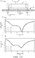
- Plot 602 indicates that the example stamped-waveguide cavity 500-2 is not as efficient as the example drawn-waveguide cavity 500-1, but still performs better than the plated slot 206 in the absence of the waveguide cavity 116. Alignment error results of the example drawn-waveguide cavity 500-1 are further described in FIGs. 7-1 , 7-2 , and 7-3 .
- FIG. 7-1 illustrates how a first alignment error 700-1 of the waveguide cavity 116 along a length axis 702 affects the reflected power 216 of S11 604 and S22 606, shown in plots 704 and 706, respectively.
- the length axis 702 is aligned with the resonant-cavity distance 238 of the planar dimension 112.
- the displacement 708 is illustrated in 700-1 for +4 mil 710. Though not shown in 700-1, the displacement 708 can include 0 mil 712, -4 mil 714, and so forth.
- Plots 704 and 706 indicate that the displacement 708 of +4 mil 710 and -4 mil 714 along the length axis 702 results in a change in the reflected power 216, both in amplitude 222 and frequency 220 of S11 604 and S22 606.
- the example drawn-waveguide cavity 500-1 with the first alignment error 700-1 still performs better than the plated slot 206 in the absence of the waveguide cavity 116.
- FIG. 7-2 illustrates how a second alignment error 700-2 of the waveguide cavity 116 along a width axis 716 affects the reflected power 216 of S11 604 and S22 606, shown in plots 718 and 720, respectively.
- the width axis 716 is aligned with the entry opening 242 of the planar dimension 112.
- Plots 718 and 720 indicate that the displacement 708 of +4 mil 710 and -4 mil 714 along the width axis 716 results in a negligible change in the reflected power 216, both in amplitude 222 and frequency 220 of S11 604 and S22 606.
- FIG. 7-3 illustrates how a third alignment error 700-3 of the waveguide cavity 116, resulting in an angular displacement 718 within the planar dimension 112, affects the reflected power 216 of S11 604 and S22 606, shown in plots 720 and 722, respectively.
- the angular displacement 718 is illustrated in 700-3 for -6 degrees 724. Though not shown in 700-3, the angular displacement 718 can include 0 degrees 726, +6 degrees 728, and so forth.
- Plots 720 and 722 indicate that the angular displacement 718 of +6 degrees 728 and -6 degrees 724 along the planar dimension 112 results in a change in the reflected power 216, both in amplitude 222 and frequency 220 of S11 604 and S22 606.
- the example drawn-waveguide cavity 500-1 with the third alignment error 700-3 still performs better than the plated slot 206 in the absence of the waveguide cavity 116.
Landscapes
- Engineering & Computer Science (AREA)
- Microelectronics & Electronic Packaging (AREA)
- Computer Security & Cryptography (AREA)
- Radar, Positioning & Navigation (AREA)
- Remote Sensing (AREA)
- Control Of Motors That Do Not Use Commutators (AREA)
- Waveguide Aerials (AREA)
- Waveguides (AREA)
Applications Claiming Priority (2)
| Application Number | Priority Date | Filing Date | Title |
|---|---|---|---|
| US202063112013P | 2020-11-10 | 2020-11-10 | |
| US17/155,949 US11757166B2 (en) | 2020-11-10 | 2021-01-22 | Surface-mount waveguide for vertical transitions of a printed circuit board |
Publications (1)
| Publication Number | Publication Date |
|---|---|
| EP3996202A1 true EP3996202A1 (fr) | 2022-05-11 |
Family
ID=78332522
Family Applications (1)
| Application Number | Title | Priority Date | Filing Date |
|---|---|---|---|
| EP21203201.5A Pending EP3996202A1 (fr) | 2020-11-10 | 2021-10-18 | Guide d'ondes à montage en surface pour transitions verticales d'une carte de circuit imprimé |
Country Status (3)
| Country | Link |
|---|---|
| US (1) | US11757166B2 (fr) |
| EP (1) | EP3996202A1 (fr) |
| CN (1) | CN114464975B (fr) |
Families Citing this family (1)
| Publication number | Priority date | Publication date | Assignee | Title |
|---|---|---|---|---|
| TWI752780B (zh) * | 2020-12-31 | 2022-01-11 | 啓碁科技股份有限公司 | 寬波束之天線結構 |
Citations (7)
| Publication number | Priority date | Publication date | Assignee | Title |
|---|---|---|---|---|
| JP2003243902A (ja) * | 2002-02-18 | 2003-08-29 | Alps Electric Co Ltd | 衛星放送受信用コンバータ |
| US6658233B1 (en) * | 1999-10-04 | 2003-12-02 | Alps Electric Co., Ltd. | Satellite broadcast receiving converter |
| US20060145777A1 (en) * | 2002-09-20 | 2006-07-06 | Eads Deutschland Gmbh | Junction between a microstrip line and a waveguide |
| US20130256849A1 (en) * | 2012-03-29 | 2013-10-03 | International Business Machines Corporation | High frequency transition matching in an electronic package for millimeter wave semiconductor dies |
| US20170099705A1 (en) * | 2014-05-26 | 2017-04-06 | Electrolux Appliances Aktiebolag | Microwave oven with a waveguide including a reflector element |
| DE102016213202A1 (de) * | 2016-07-19 | 2018-01-25 | Conti Temic Microelectronic Gmbh | Mehrschichtenplatine mit einem Übergangselement zum Transformieren einer Hohlleiterwelle auf eine leitungsgeführte Welle |
| CN109750201A (zh) * | 2019-02-22 | 2019-05-14 | 中国科学院长春应用化学研究所 | 一种高成型性能微合金化镁合金薄板及其制备方法 |
Family Cites Families (203)
| Publication number | Priority date | Publication date | Assignee | Title |
|---|---|---|---|---|
| US2840818A (en) | 1954-04-15 | 1958-06-24 | Hughes Aircraft Co | Slotted antenna |
| US3462713A (en) | 1967-07-19 | 1969-08-19 | Bell Telephone Labor Inc | Waveguide-stripline transducer |
| US3579149A (en) | 1969-12-08 | 1971-05-18 | Westinghouse Electric Corp | Waveguide to stripline transition means |
| NL7609903A (nl) | 1976-09-07 | 1978-03-09 | Philips Nv | Microgolfinrichting voor het omzetten van een golfpijp- in een microstripgeleiderstructuur. |
| US4453142A (en) | 1981-11-02 | 1984-06-05 | Motorola Inc. | Microstrip to waveguide transition |
| US4562416A (en) | 1984-05-31 | 1985-12-31 | Sanders Associates, Inc. | Transition from stripline to waveguide |
| JP2932650B2 (ja) | 1990-09-17 | 1999-08-09 | 松下電器産業株式会社 | 微細構造物の製造方法 |
| US5065123A (en) | 1990-10-01 | 1991-11-12 | Harris Corporation | Waffle wall-configured conducting structure for chip isolation in millimeter wave monolithic subsystem assemblies |
| DE4241635C2 (de) | 1992-12-10 | 1994-11-10 | Ant Nachrichtentech | Übergang von einer Microstrip-Leitung auf einen Hohlleiter |
| FR2700066A1 (fr) | 1992-12-29 | 1994-07-01 | Philips Electronique Lab | Dispositif hyperfréquences comprenant au moins une transition entre une ligne de transmission intégrée sur un substrat et un guide d'onde. |
| US5986527A (en) | 1995-03-28 | 1999-11-16 | Murata Manufacturing Co., Ltd. | Planar dielectric line and integrated circuit using the same line |
| US5637521A (en) | 1996-06-14 | 1997-06-10 | The United States Of America As Represented By The Secretary Of The Army | Method of fabricating an air-filled waveguide on a semiconductor body |
| JP3366552B2 (ja) | 1997-04-22 | 2003-01-14 | 京セラ株式会社 | 誘電体導波管線路およびそれを具備する多層配線基板 |
| US5929728A (en) | 1997-06-25 | 1999-07-27 | Hewlett-Packard Company | Imbedded waveguide structures for a microwave circuit package |
| EP0893842B1 (fr) | 1997-07-25 | 2004-05-06 | Kyocera Corporation | Antenne à ouverture stratifiée et panneau à circuit multicouche comprenant la dite antenne |
| US5923225A (en) | 1997-10-03 | 1999-07-13 | De Los Santos; Hector J. | Noise-reduction systems and methods using photonic bandgap crystals |
| US5982250A (en) | 1997-11-26 | 1999-11-09 | Twr Inc. | Millimeter-wave LTCC package |
| US6072375A (en) | 1998-05-12 | 2000-06-06 | Harris Corporation | Waveguide with edge grounding |
| CA2292064C (fr) | 1998-12-25 | 2003-08-19 | Murata Manufacturing Co., Ltd. | Dispositif de transition de ligne entre un guide d'ondes dielectrique, et un guide d'ondes, et oscillateur et emetteur utilisant ce meme dispositif |
| US6127901A (en) | 1999-05-27 | 2000-10-03 | Hrl Laboratories, Llc | Method and apparatus for coupling a microstrip transmission line to a waveguide transmission line for microwave or millimeter-wave frequency range transmission |
| JP2000357916A (ja) | 1999-06-15 | 2000-12-26 | Kobe Steel Ltd | 導波管スロットアレーアンテナ |
| US6590477B1 (en) | 1999-10-29 | 2003-07-08 | Fci Americas Technology, Inc. | Waveguides and backplane systems with at least one mode suppression gap |
| US6414573B1 (en) | 2000-02-16 | 2002-07-02 | Hughes Electronics Corp. | Stripline signal distribution system for extremely high frequency signals |
| US6622370B1 (en) | 2000-04-13 | 2003-09-23 | Raytheon Company | Method for fabricating suspended transmission line |
| US6535083B1 (en) | 2000-09-05 | 2003-03-18 | Northrop Grumman Corporation | Embedded ridge waveguide filters |
| CN1274056C (zh) | 2000-10-18 | 2006-09-06 | 诺基亚公司 | 波导到带状线转接 |
| US6794950B2 (en) | 2000-12-21 | 2004-09-21 | Paratek Microwave, Inc. | Waveguide to microstrip transition |
| KR100450376B1 (ko) | 2001-01-12 | 2004-09-30 | 가부시키가이샤 무라타 세이사쿠쇼 | 전송 선로, 집적회로 및 송수신 장치 |
| US6967347B2 (en) | 2001-05-21 | 2005-11-22 | The Regents Of The University Of Colorado | Terahertz interconnect system and applications |
| KR20030031585A (ko) | 2001-10-15 | 2003-04-23 | (주)지앤티웍스 | 슬롯 배열 안테나의 제작을 위한 양면 유전체 기판의도파관 부착 기법 |
| EP1331688A1 (fr) | 2002-01-29 | 2003-07-30 | Era Patents Limited | Guide d'onde |
| JP2003289201A (ja) | 2002-03-28 | 2003-10-10 | Anritsu Corp | ポスト壁導波管と空洞導波管の接続変換構造 |
| JP3923360B2 (ja) | 2002-04-26 | 2007-05-30 | 三菱電機株式会社 | スロットアレーアンテナ及びスロットアレーアンテナ装置 |
| CA2430795A1 (fr) | 2002-05-31 | 2003-11-30 | George V. Eleftheriades | Metamateriaux planaires pour commander et guider le rayonnement electromagnetique et applications connexes |
| US7157992B2 (en) | 2004-03-08 | 2007-01-02 | Wemtec, Inc. | Systems and methods for blocking microwave propagation in parallel plate structures |
| US7276988B2 (en) | 2004-06-30 | 2007-10-02 | Endwave Corporation | Multi-substrate microstrip to waveguide transition |
| US6995726B1 (en) | 2004-07-15 | 2006-02-07 | Rockwell Collins | Split waveguide phased array antenna with integrated bias assembly |
| US7098070B2 (en) | 2004-11-16 | 2006-08-29 | International Business Machines Corporation | Device and method for fabricating double-sided SOI wafer scale package with through via connections |
| CN2796131Y (zh) | 2005-05-30 | 2006-07-12 | 东南大学 | 多层基片集成波导椭圆响应滤波器 |
| JP4395103B2 (ja) | 2005-06-06 | 2010-01-06 | 富士通株式会社 | 導波路基板および高周波回路モジュール |
| US7420442B1 (en) | 2005-06-08 | 2008-09-02 | Sandia Corporation | Micromachined microwave signal control device and method for making same |
| KR100651627B1 (ko) | 2005-11-25 | 2006-12-01 | 한국전자통신연구원 | 교차결합을 갖는 유전체 도파관 필터 |
| KR101168608B1 (ko) | 2006-03-31 | 2012-07-30 | 쿄세라 코포레이션 | 유전체 도파로 디바이스와, 이것을 구비하는 이상기, 고주파 스위치 및 감쇠기와, 고주파 송신기, 고주파 수신기, 고주파 송수신기, 레이더 장치, 어레이 안테나 장치, 및 유전체 도파로 디바이스의 제조 방법 |
| KR100731544B1 (ko) | 2006-04-13 | 2007-06-22 | 한국전자통신연구원 | 다층배선 코플래너 웨이브가이드 |
| AU2007261114B2 (en) | 2006-06-12 | 2012-07-12 | Pacific Biosciences Of California, Inc. | Substrates for performing analytical reactions |
| KR100846872B1 (ko) | 2006-11-17 | 2008-07-16 | 한국전자통신연구원 | 유전체 도파관 대 전송선의 밀리미터파 천이 장치 |
| JP4365852B2 (ja) | 2006-11-30 | 2009-11-18 | 株式会社日立製作所 | 導波管構造 |
| EP1936741A1 (fr) | 2006-12-22 | 2008-06-25 | Sony Deutschland GmbH | Guides d'ondes intégrés dans un substrat flexible |
| US8231284B2 (en) | 2007-03-26 | 2012-07-31 | International Business Machines Corporation | Ultra-high bandwidth, multiple-channel full-duplex, single-chip CMOS optical transceiver |
| US7768457B2 (en) | 2007-06-22 | 2010-08-03 | Vubiq, Inc. | Integrated antenna and chip package and method of manufacturing thereof |
| US20090040132A1 (en) | 2007-07-24 | 2009-02-12 | Northeastern University | Anisotropic metal-dielectric metamaterials for broadband all-angle negative refraction and superlens imaging |
| WO2009084697A1 (fr) | 2007-12-28 | 2009-07-09 | Kyocera Corporation | Structure de connexion de ligne de transmission haute fréquence, substrat de câblage, module haute fréquence et dispositif radar |
| EP2269266A4 (fr) | 2008-03-25 | 2014-07-09 | Tyco Electronics Services Gmbh | Systèmes d'antenne à métamatériau actif d'avant-garde |
| CA2629035A1 (fr) | 2008-03-27 | 2009-09-27 | Her Majesty The Queen In Right Of Canada, As Represented By The Minister Of Industry, Through The Communications Research Centre Canada | Filtre de guide d'ondes avec large bande affaiblie, reposant sur un mecanisme de substrat de guide d'ondes integre |
| JP5172481B2 (ja) | 2008-06-05 | 2013-03-27 | 株式会社東芝 | ポスト壁導波路によるショートスロット方向性結合器とこれを用いたバトラーマトリクス及び車載レーダアンテナ |
| JP5616338B2 (ja) | 2008-07-07 | 2014-10-29 | キルダル アンテナ コンサルティング アクティエボラーグ | 平行な伝導表面間のギャップにおける導波管と伝送ライン |
| WO2010065071A2 (fr) | 2008-11-25 | 2010-06-10 | Regents Of The University Of Minnesota | Réplication de structures à film mince à motifs destinées à être utilisées en plasmonique et dans les métamatériaux |
| US8278749B2 (en) | 2009-01-30 | 2012-10-02 | Infineon Technologies Ag | Integrated antennas in wafer level package |
| US8089327B2 (en) | 2009-03-09 | 2012-01-03 | Toyota Motor Engineering & Manufacturing North America, Inc. | Waveguide to plural microstrip transition |
| JP5309209B2 (ja) | 2009-03-31 | 2013-10-09 | 京セラ株式会社 | 導波構造体、ならびに、導波構造体を含む高周波モジュールおよびレーダ装置 |
| CN201383535Y (zh) | 2009-04-01 | 2010-01-13 | 惠州市硕贝德通讯科技有限公司 | 一种矩形波导-基片集成波导信号转换及功率分配器 |
| US8451189B1 (en) | 2009-04-15 | 2013-05-28 | Herbert U. Fluhler | Ultra-wide band (UWB) artificial magnetic conductor (AMC) metamaterials for electrically thin antennas and arrays |
| US8901719B2 (en) | 2009-05-08 | 2014-12-02 | Optis Cellular Technology, Llc | Transition from a chip to a waveguide port |
| US8917151B2 (en) | 2009-09-08 | 2014-12-23 | Siklu Communication ltd. | Transition between a laminated PCB and a waveguide through a cavity in the laminated PCB |
| US8912859B2 (en) | 2009-09-08 | 2014-12-16 | Siklu Communication ltd. | Transition between a laminated PCB and a waveguide including a lamina with a printed conductive surface functioning as a waveguide-backshort |
| FR2953651B1 (fr) | 2009-12-07 | 2012-01-20 | Eads Defence & Security Sys | Dispositif de transition hyperfrequence entre une ligne a micro-ruban et un guide d'onde rectangulaire |
| JP5639194B2 (ja) | 2010-01-22 | 2014-12-10 | ヌボトロニクス,エルエルシー | 熱制御 |
| US9774076B2 (en) | 2010-08-31 | 2017-09-26 | Siklu Communication ltd. | Compact millimeter-wave radio systems and methods |
| US8674885B2 (en) | 2010-08-31 | 2014-03-18 | Siklu Communication ltd. | Systems for interfacing waveguide antenna feeds with printed circuit boards |
| WO2012071340A1 (fr) | 2010-11-23 | 2012-05-31 | Metamagnetics Inc. | Module d'antenne de taille réduite, à gain élevé, et à rendement de puissance accru |
| KR101761920B1 (ko) | 2011-02-16 | 2017-07-26 | 삼성전기주식회사 | 유전체 도파관 안테나 |
| US9270005B2 (en) | 2011-02-21 | 2016-02-23 | Siklu Communication ltd. | Laminate structures having a hole surrounding a probe for propagating millimeter waves |
| EP2500978B1 (fr) | 2011-03-17 | 2013-07-10 | Sivers Ima AB | Transition de guide d'onde |
| GB2489950A (en) | 2011-04-12 | 2012-10-17 | Filtronic Plc | A substrate integrated waveguide (SIW) to air filled waveguide transition comprising a tapered dielectric layer |
| KR20130007690A (ko) | 2011-06-27 | 2013-01-21 | 한국전자통신연구원 | 메타물질 구조체 및 그의 제조방법 |
| US9147924B2 (en) | 2011-09-02 | 2015-09-29 | The United States Of America As Represented By The Secretary Of The Army | Waveguide to co-planar-waveguide (CPW) transition |
| US8680936B2 (en) | 2011-11-18 | 2014-03-25 | Delphi Technologies, Inc. | Surface mountable microwave signal transition block for microstrip to perpendicular waveguide transition |
| EP2618421A1 (fr) | 2012-01-19 | 2013-07-24 | Huawei Technologies Co., Ltd. | Système à micro-ondes monté en surface |
| US9246204B1 (en) | 2012-01-19 | 2016-01-26 | Hrl Laboratories, Llc | Surface wave guiding apparatus and method for guiding the surface wave along an arbitrary path |
| FR2989842B1 (fr) | 2012-04-24 | 2015-07-17 | Univ Joseph Fourier | Ligne de propagation radiofrequence a ondes lentes |
| JP5969816B2 (ja) | 2012-05-17 | 2016-08-17 | キヤノン株式会社 | 構造部材及び通信装置 |
| CN104488134A (zh) | 2012-06-18 | 2015-04-01 | 加普韦夫斯公司 | 用于THz应用的间隙波导结构 |
| WO2013189513A1 (fr) | 2012-06-18 | 2013-12-27 | Huawei Technologies Co., Ltd. | Structure de guide d'onde de coupleur directionnel et procédé associé |
| JP5694246B2 (ja) | 2012-07-13 | 2015-04-01 | 株式会社東芝 | 導波管接続構造、アンテナ装置およびレーダ装置 |
| US8969730B2 (en) | 2012-08-16 | 2015-03-03 | Apple Inc. | Printed circuit solder connections |
| US20140106684A1 (en) | 2012-10-15 | 2014-04-17 | Qualcomm Mems Technologies, Inc. | Transparent antennas on a display device |
| US9356352B2 (en) | 2012-10-22 | 2016-05-31 | Texas Instruments Incorporated | Waveguide coupler |
| JP2016503245A (ja) | 2013-01-10 | 2016-02-01 | 日本電気株式会社 | 平面伝送線路および導波管の間の広帯域変換器 |
| US10312596B2 (en) | 2013-01-17 | 2019-06-04 | Hrl Laboratories, Llc | Dual-polarization, circularly-polarized, surface-wave-waveguide, artificial-impedance-surface antenna |
| US9831565B2 (en) | 2013-03-24 | 2017-11-28 | Telefonaktiebolaget Lm Ericsson (Publ) | SIW antenna arrangement |
| WO2014154232A1 (fr) | 2013-03-24 | 2014-10-02 | Telefonaktiebolaget L M Ericsson (Publ) | Transition entre un siw et une interface de guide d'ondes |
| CN103515682B (zh) | 2013-07-24 | 2015-07-29 | 中国电子科技集团公司第五十五研究所 | 多层阶梯式基片集成波导实现微带至波导的垂直过渡结构 |
| WO2015013927A1 (fr) | 2013-07-31 | 2015-02-05 | 华为技术有限公司 | Antenne |
| EP2843758A1 (fr) | 2013-08-27 | 2015-03-04 | Microelectronics Technology Inc. | Carte de circuit imprimé multicouche avec guide d'onde vers une structure de transition de microbande |
| CN105580195B (zh) | 2013-10-01 | 2019-07-16 | 索尼半导体解决方案公司 | 连接器装置和通信系统 |
| US9059490B2 (en) | 2013-10-08 | 2015-06-16 | Blackberry Limited | 60 GHz integrated circuit to printed circuit board transitions |
| JP6269127B2 (ja) | 2014-02-07 | 2018-01-31 | 富士通株式会社 | 高周波モジュール及びその製造方法 |
| CN103762416B (zh) * | 2014-02-25 | 2016-12-07 | 中国工程物理研究院电子工程研究所 | 一种太赫兹波片载-波导-喇叭转换天线 |
| US9548523B2 (en) | 2014-04-09 | 2017-01-17 | Texas Instruments Incorporated | Waveguide formed with a dielectric core surrounded by conductive layers including a conformal base layer that matches the footprint of the waveguide |
| WO2015170717A1 (fr) | 2014-05-07 | 2015-11-12 | 桐野秀樹 | Guide d'ondes et son dispositif |
| JP6607869B2 (ja) | 2014-05-14 | 2019-11-20 | ギャップウエイブス アクチボラグ | 平行導電面間の間隙に設けられる導波路及び伝送線路 |
| EP2945222A1 (fr) | 2014-05-14 | 2015-11-18 | Gapwaves AB | Partie RF de four à micro-ondes ou d'ondes millimétriques utilisant des technologies de matrice de broches (PGA) et/ou de grille matricielle à billes (BGA) |
| US10177430B2 (en) | 2014-05-16 | 2019-01-08 | City University Of Hong Kong | Apparatus and a method for electromagnetic signal transition |
| US10983194B1 (en) | 2014-06-12 | 2021-04-20 | Hrl Laboratories, Llc | Metasurfaces for improving co-site isolation for electronic warfare applications |
| US9620841B2 (en) | 2014-06-13 | 2017-04-11 | Nxp Usa, Inc. | Radio frequency coupling structure |
| US10103447B2 (en) | 2014-06-13 | 2018-10-16 | Nxp Usa, Inc. | Integrated circuit package with radio frequency coupling structure |
| US9583811B2 (en) | 2014-08-07 | 2017-02-28 | Infineon Technologies Ag | Transition between a plastic waveguide and a semiconductor chip, where the semiconductor chip is embedded and encapsulated within a mold compound |
| KR101621480B1 (ko) | 2014-10-16 | 2016-05-16 | 현대모비스 주식회사 | 도파관 대 유전체 도파관의 천이 구조 |
| US9666930B2 (en) | 2014-10-23 | 2017-05-30 | Nxp Usa, Inc. | Interface between a semiconductor die and a waveguide, where the interface is covered by a molding compound |
| US10522895B2 (en) | 2014-12-12 | 2019-12-31 | Sony Corporation | Microwave antenna apparatus, packing and manufacturing method |
| US9537199B2 (en) | 2015-03-19 | 2017-01-03 | International Business Machines Corporation | Package structure having an integrated waveguide configured to communicate between first and second integrated circuit chips |
| US10109604B2 (en) | 2015-03-30 | 2018-10-23 | Sony Corporation | Package with embedded electronic components and a waveguide cavity through the package cover, antenna apparatus including package, and method of manufacturing the same |
| JP6778695B2 (ja) | 2015-04-08 | 2020-11-04 | ギャップウェーブス アーベー | マイクロ波解析機器またはマイクロ波測定機器用の較正装置 |
| KR101689353B1 (ko) | 2015-04-13 | 2016-12-23 | 성균관대학교산학협력단 | 실리콘 밀리미터파 칩용 칩상 도파관 급전기 및 급전 방법 및, 이를 이용한 다중 입출력 밀리미터파 송수신 장치 |
| CN104900956A (zh) | 2015-05-06 | 2015-09-09 | 东南大学 | 一种波导到基片集成波导的转换装置 |
| CN106487353B (zh) | 2015-08-28 | 2021-09-28 | 香港城市大学深圳研究院 | 将单端信号转换为差分信号的装置、方法以及系统 |
| US10083923B2 (en) | 2015-09-21 | 2018-09-25 | Intel Corporation | Platform with thermally stable wireless interconnects |
| EP3147994B1 (fr) | 2015-09-24 | 2019-04-03 | Gapwaves AB | Guides d'ondes et lignes de transmission dans des interstices entre des surfaces conductrices parallèles |
| US10833382B2 (en) | 2015-09-25 | 2020-11-10 | Bae Systems Australia Limited | RF structure and a method of forming an RF structure |
| DE102016119473B4 (de) | 2015-10-15 | 2022-10-20 | Nidec Elesys Corporation | Wellenleitervorrichtung und Antennenvorrichtung mit der Wellenleitervorrichtung |
| CN207542369U (zh) | 2015-11-05 | 2018-06-26 | 日本电产株式会社 | 雷达系统以及无线通信系统 |
| DE112016000180B4 (de) | 2015-11-05 | 2023-08-03 | Nidec Corporation | Schlitz-Array-Antenne |
| US10381741B2 (en) | 2015-12-24 | 2019-08-13 | Nidec Corporation | Slot array antenna, and radar, radar system, and wireless communication system including the slot array antenna |
| JP2017188867A (ja) | 2015-12-24 | 2017-10-12 | 日本電産エレシス株式会社 | 導波路装置、スロットアンテナ、ならびに当該スロットアンテナを備えるレーダ、レーダシステム、および無線通信システム |
| CN105680133B (zh) | 2016-01-11 | 2018-08-10 | 中国电子科技集团公司第十研究所 | 基片集成脊波导板间垂直互联电路结构 |
| CN206774650U (zh) | 2016-01-15 | 2017-12-19 | 日本电产艾莱希斯株式会社 | 波导装置、天线装置以及雷达 |
| CN108475833A (zh) | 2016-01-20 | 2018-08-31 | 索尼公司 | 连接器模块、通信电路板和电子装置 |
| US10114067B2 (en) | 2016-02-04 | 2018-10-30 | Advantest Corporation | Integrated waveguide structure and socket structure for millimeter waveband testing |
| DE102017102284A1 (de) | 2016-02-08 | 2017-08-10 | Nidec Elesys Corporation | Wellenleitervorrichtung und Antennenvorrichtung mit der Wellenleitervorrichtung |
| DE102017102559A1 (de) | 2016-02-12 | 2017-08-17 | Nidec Elesys Corporation | Wellenleitervorrichtung und Antennenvorrichtung mit der Wellenleitervorrichtung |
| EP3414789B1 (fr) | 2016-02-12 | 2021-10-06 | Telefonaktiebolaget LM Ericsson (publ) | Agencement de transition comprenant une transition ou une connexion sans contact entre un siw et un guide d'ondes ou une antenne |
| CN105609909A (zh) | 2016-03-08 | 2016-05-25 | 电子科技大学 | 一种用于Ka波段矩形波导转基片集成波导的装置 |
| JP2019047141A (ja) | 2016-03-29 | 2019-03-22 | 日本電産エレシス株式会社 | マイクロ波ic導波路装置モジュール、レーダ装置およびレーダシステム |
| JP6910374B2 (ja) | 2016-04-05 | 2021-07-28 | 日本電産株式会社 | 導波路装置およびアンテナアレイ |
| JP2019054315A (ja) | 2016-04-28 | 2019-04-04 | 日本電産エレシス株式会社 | 実装基板、導波路モジュール、集積回路実装基板、マイクロ波モジュール、レーダ装置およびレーダシステム |
| WO2017192071A1 (fr) | 2016-05-03 | 2017-11-09 | Gapwaves Ab | Agencement permettant l'interconnexion de structures de guide d'ondes et structure permettant un agencement d'interconnexion de structures de guide d'ondes |
| US9947981B1 (en) | 2016-05-19 | 2018-04-17 | National Technology & Engineering Solutions of Sandian, LLC | Waveguide module comprising a first plate with a waveguide channel and a second plate with a raised portion in which a sealing layer is forced into the waveguide channel by the raised portion |
| CN208955165U (zh) | 2016-06-29 | 2019-06-07 | 日本电产株式会社 | 雷达装置 |
| CN105958167B (zh) | 2016-07-01 | 2019-03-05 | 北京交通大学 | 垂直基片集成波导及包括该波导的垂直连接结构 |
| US9843301B1 (en) | 2016-07-14 | 2017-12-12 | Northrop Grumman Systems Corporation | Silicon transformer balun |
| US10505282B2 (en) | 2016-08-10 | 2019-12-10 | Microsoft Technology Licensing, Llc | Dielectric groove waveguide |
| JP2019526670A (ja) | 2016-08-22 | 2019-09-19 | エムエーペー ウーロペ ベスローテン フェンノートシャップ | レーザーダイレクトストラクチャリング用熱可塑性組成物 |
| KR101781477B1 (ko) * | 2016-09-19 | 2017-10-23 | 유한회사 에스피앤파트너스 | 전자 레인지 및 그의 방사 모듈 |
| EP3301758A1 (fr) | 2016-09-30 | 2018-04-04 | IMS Connector Systems GmbH | Élément d'antenne |
| US10811373B2 (en) | 2016-10-05 | 2020-10-20 | Gapwaves Ab | Packaging structure comprising at least one transition forming a contactless interface |
| US11249011B2 (en) | 2016-10-19 | 2022-02-15 | Global Life Sciences Solutions Usa Llc | Apparatus and method for evanescent waveguide sensing |
| KR101963936B1 (ko) | 2016-11-08 | 2019-07-31 | 한국과학기술원 | 전자파 신호 송수신 안테나 및 em-터널이 내장된 구조를 갖는 인쇄회로기판 및 그 제작 방법 |
| CN106785424B (zh) * | 2016-11-29 | 2019-07-12 | 大连港森立达木材交易中心有限公司 | 高功率微波双向均匀辐照天馈系统 |
| US9935065B1 (en) | 2016-12-21 | 2018-04-03 | Infineon Technologies Ag | Radio frequency device packages and methods of formation thereof |
| CN110168801B (zh) | 2017-01-24 | 2021-07-27 | 胡贝尔舒纳公司 | 波导组件和用于电磁信号传输的方法 |
| JP2018129623A (ja) | 2017-02-07 | 2018-08-16 | パナソニック株式会社 | モジュール、無線通信装置、および、レーダ装置 |
| US10468736B2 (en) | 2017-02-08 | 2019-11-05 | Aptiv Technologies Limited | Radar assembly with ultra wide band waveguide to substrate integrated waveguide transition |
| EP3364457A1 (fr) | 2017-02-15 | 2018-08-22 | Nxp B.V. | Conditionnement de circuit intégré avec antenne |
| JP2018164252A (ja) | 2017-03-24 | 2018-10-18 | 日本電産株式会社 | スロットアレーアンテナ、および当該スロットアレーアンテナを備えるレーダ |
| US10317459B2 (en) | 2017-04-03 | 2019-06-11 | Nvidia Corporation | Multi-chip package with selection logic and debug ports for testing inter-chip communications |
| CN108695585B (zh) | 2017-04-12 | 2021-03-16 | 日本电产株式会社 | 高频构件的制造方法 |
| JP7020677B2 (ja) | 2017-04-13 | 2022-02-16 | 日本電産エレシス株式会社 | スロットアンテナ装置 |
| US10608345B2 (en) | 2017-04-13 | 2020-03-31 | Nidec Corporation | Slot array antenna |
| CN208093762U (zh) | 2017-04-14 | 2018-11-13 | 日本电产株式会社 | 缝隙天线装置以及雷达装置 |
| JP7129999B2 (ja) | 2017-05-11 | 2022-09-02 | 日本電産株式会社 | 導波路装置および当該導波路装置を備えるアンテナ装置 |
| DE102017111319A1 (de) | 2017-05-24 | 2018-11-29 | Miele & Cie. Kg | Einrichtung zur Erzeugung und Transmission von Hochfrequenzwellen (HF-Wellen) |
| JP2018207487A (ja) | 2017-06-05 | 2018-12-27 | 日本電産株式会社 | 導波路装置および当該導波路装置を備えるアンテナ装置 |
| US10547122B2 (en) | 2017-06-26 | 2020-01-28 | Nidec Corporation | Method of producing a horn antenna array and antenna array |
| JP7103860B2 (ja) | 2017-06-26 | 2022-07-20 | 日本電産エレシス株式会社 | ホーンアンテナアレイ |
| US20180375185A1 (en) | 2017-06-26 | 2018-12-27 | WGR Co., Ltd. | Electromagnetic wave transmission device |
| JP2019009779A (ja) | 2017-06-26 | 2019-01-17 | 株式会社Wgr | 伝送線路装置 |
| JP2019012999A (ja) | 2017-06-30 | 2019-01-24 | 日本電産株式会社 | 導波路装置モジュール、マイクロ波モジュール、レーダ装置およびレーダシステム |
| US20200153108A1 (en) | 2017-07-06 | 2020-05-14 | Fujikura Ltd. | Waveguide slot array antenna |
| JP7294608B2 (ja) | 2017-08-18 | 2023-06-20 | ニデックエレシス株式会社 | アンテナアレイ |
| JP2019050568A (ja) | 2017-09-07 | 2019-03-28 | 日本電産株式会社 | 方向性結合器 |
| US11183751B2 (en) | 2017-09-20 | 2021-11-23 | Aptiv Technologies Limited | Antenna device with direct differential input useable on an automated vehicle |
| ES2886940T3 (es) | 2017-09-25 | 2021-12-21 | Gapwaves Ab | Red de antenas en fase |
| US11289787B2 (en) | 2017-10-25 | 2022-03-29 | Gapwaves Ab | Transition arrangement comprising a waveguide twist, a waveguide structure comprising a number of waveguide twists and a rotary joint |
| SE541861C2 (en) | 2017-10-27 | 2019-12-27 | Metasum Ab | Multi-layer waveguide, arrangement, and method for production thereof |
| CN107946717A (zh) | 2017-10-31 | 2018-04-20 | 深圳市华讯方舟微电子科技有限公司 | 威尔金森功分器 |
| EP3707540A4 (fr) | 2017-11-07 | 2021-07-21 | Rahiminejad, Sofia | Commutateur de guide d'ondes sans contact et procédé de fabrication d'un commutateur de guide d'ondes |
| KR102342520B1 (ko) | 2017-11-10 | 2021-12-22 | 레이던 컴퍼니 | 밀리미터파 전송 라인 구조 |
| ES2792043T3 (es) * | 2017-12-04 | 2020-11-06 | Grieshaber Vega Kg | Placa de circuitos impresos para un aparato de medición de nivel de llenado por radar con un acoplamiento de guía de ondas |
| US10670810B2 (en) | 2017-12-22 | 2020-06-02 | Huawei Technologies Canada Co., Ltd. | Polarization selective coupler |
| US10403954B2 (en) | 2017-12-30 | 2019-09-03 | Texas Instruments Incorporated | Printed circuit board with substrate-integrated waveguide transition |
| FR3079036A1 (fr) | 2018-03-15 | 2019-09-20 | Stmicroelectronics (Crolles 2) Sas | Dispositif de filtrage dans un guide d'onde |
| FR3079037B1 (fr) | 2018-03-15 | 2020-09-04 | St Microelectronics Crolles 2 Sas | Dispositif de terminaison de guide d'onde |
| JP7298808B2 (ja) | 2018-06-14 | 2023-06-27 | ニデックエレシス株式会社 | スロットアレイアンテナ |
| EP3621146B1 (fr) | 2018-09-04 | 2023-10-11 | Gapwaves AB | Filtre à haute fréquence et antenne réseau à commande de phase comprenant un tel filtre à haute fréquence |
| RU2696676C1 (ru) | 2018-12-06 | 2019-08-05 | Самсунг Электроникс Ко., Лтд. | Гребневый волновод без боковых стенок на базе печатной платы и содержащая его многослойная антенная решетка |
| US11201414B2 (en) | 2018-12-18 | 2021-12-14 | Veoneer Us, Inc. | Waveguide sensor assemblies and related methods |
| JP7379176B2 (ja) | 2019-01-16 | 2023-11-14 | 太陽誘電株式会社 | 導波路装置、電磁波閉じ込め装置、アンテナ装置、マイクロ波化学反応装置、およびレーダ装置 |
| DE102019200893B4 (de) | 2019-01-21 | 2023-06-15 | Infineon Technologies Ag | Verfahren zum Erzeugen eines Hohlleiters, Schaltungsvorrichtung und Radarsystem |
| SE1930047A1 (en) | 2019-02-08 | 2020-06-30 | Gapwaves Ab | Antenna array based on one or more metamaterial structures |
| CN209389219U (zh) | 2019-02-25 | 2019-09-13 | 贵州航天电子科技有限公司 | 一种适用于增材制造的波导缝隙阵列天线结构 |
| US10944184B2 (en) | 2019-03-06 | 2021-03-09 | Aptiv Technologies Limited | Slot array antenna including parasitic features |
| US10775573B1 (en) | 2019-04-03 | 2020-09-15 | International Business Machines Corporation | Embedding mirror with metal particle coating |
| US11527808B2 (en) | 2019-04-29 | 2022-12-13 | Aptiv Technologies Limited | Waveguide launcher |
| US10903581B2 (en) | 2019-06-26 | 2021-01-26 | Honeywell International Inc. | Fixing structure to enhance the mechanical reliability of plate slot array antenna based on SIW technology |
| US11283162B2 (en) | 2019-07-23 | 2022-03-22 | Veoneer Us, Inc. | Transitional waveguide structures and related sensor assemblies |
| US11196171B2 (en) | 2019-07-23 | 2021-12-07 | Veoneer Us, Inc. | Combined waveguide and antenna structures and related sensor assemblies |
| US11171399B2 (en) | 2019-07-23 | 2021-11-09 | Veoneer Us, Inc. | Meandering waveguide ridges and related sensor assemblies |
| US10957971B2 (en) | 2019-07-23 | 2021-03-23 | Veoneer Us, Inc. | Feed to waveguide transition structures and related sensor assemblies |
| US11114733B2 (en) | 2019-07-23 | 2021-09-07 | Veoneer Us, Inc. | Waveguide interconnect transitions and related sensor assemblies |
| US20230036066A1 (en) | 2019-12-20 | 2023-02-02 | Gapwaves Ab | An antenna arrangement with a low-ripple radiation pattern |
| US11349220B2 (en) | 2020-02-12 | 2022-05-31 | Veoneer Us, Inc. | Oscillating waveguides and related sensor assemblies |
| US11563259B2 (en) | 2020-02-12 | 2023-01-24 | Veoneer Us, Llc | Waveguide signal confinement structures and related sensor assemblies |
| US11378683B2 (en) | 2020-02-12 | 2022-07-05 | Veoneer Us, Inc. | Vehicle radar sensor assemblies |
-
2021
- 2021-01-22 US US17/155,949 patent/US11757166B2/en active Active
- 2021-10-18 EP EP21203201.5A patent/EP3996202A1/fr active Pending
- 2021-11-09 CN CN202111321802.9A patent/CN114464975B/zh active Active
Patent Citations (7)
| Publication number | Priority date | Publication date | Assignee | Title |
|---|---|---|---|---|
| US6658233B1 (en) * | 1999-10-04 | 2003-12-02 | Alps Electric Co., Ltd. | Satellite broadcast receiving converter |
| JP2003243902A (ja) * | 2002-02-18 | 2003-08-29 | Alps Electric Co Ltd | 衛星放送受信用コンバータ |
| US20060145777A1 (en) * | 2002-09-20 | 2006-07-06 | Eads Deutschland Gmbh | Junction between a microstrip line and a waveguide |
| US20130256849A1 (en) * | 2012-03-29 | 2013-10-03 | International Business Machines Corporation | High frequency transition matching in an electronic package for millimeter wave semiconductor dies |
| US20170099705A1 (en) * | 2014-05-26 | 2017-04-06 | Electrolux Appliances Aktiebolag | Microwave oven with a waveguide including a reflector element |
| DE102016213202A1 (de) * | 2016-07-19 | 2018-01-25 | Conti Temic Microelectronic Gmbh | Mehrschichtenplatine mit einem Übergangselement zum Transformieren einer Hohlleiterwelle auf eine leitungsgeführte Welle |
| CN109750201A (zh) * | 2019-02-22 | 2019-05-14 | 中国科学院长春应用化学研究所 | 一种高成型性能微合金化镁合金薄板及其制备方法 |
Also Published As
| Publication number | Publication date |
|---|---|
| CN114464975B (zh) | 2024-08-30 |
| US11757166B2 (en) | 2023-09-12 |
| CN114464975A (zh) | 2022-05-10 |
| US20220151074A1 (en) | 2022-05-12 |
Similar Documents
| Publication | Publication Date | Title |
|---|---|---|
| JP5147826B2 (ja) | ミリ波用途のための導波管−平面伝送線路変換器を構築し、パッケージするための装置及び方法 | |
| US9490768B2 (en) | High frequency band pass filter with coupled surface mount transition | |
| US9647313B2 (en) | Surface mount microwave system including a transition between a multilayer arrangement and a hollow waveguide | |
| JP5431433B2 (ja) | 高周波線路−導波管変換器 | |
| EP3252870B1 (fr) | Module d'antenne | |
| EP1923950A1 (fr) | Ensemble microondes compatible SMT avec interface de guide d'ondes | |
| CN100418263C (zh) | 半模基片集成波导 | |
| WO2023093690A1 (fr) | Carte de circuit imprimé et dispositif électronique | |
| EP3996202A1 (fr) | Guide d'ondes à montage en surface pour transitions verticales d'une carte de circuit imprimé | |
| KR101914014B1 (ko) | 기판 집적형 도파관 구조를 갖는 밀리미터파 서큘레이터 | |
| KR20180088002A (ko) | 전송선로-도파관 전이 장치 | |
| JP6311822B2 (ja) | 高周波モジュール | |
| CN112290221B (zh) | 一种毫米波复合基片集成波导缝隙天线 | |
| CN212908021U (zh) | 基于htcc工艺的三维垂直互联结构及t/r组件 | |
| CN113540768B (zh) | 一种应用于微波系统的连接结构 | |
| CN108682945A (zh) | 一种喇叭天线及其制备方法 | |
| JP6135485B2 (ja) | 高周波モジュール | |
| JP2006279199A (ja) | 高周波線路−導波管変換器 | |
| JP4749234B2 (ja) | 開口面アンテナ | |
| CN114221108B (zh) | 传输装置 | |
| CN217507641U (zh) | 一种平面微带转间隙波导天线 | |
| CN219227952U (zh) | 一种集成耦合结构 | |
| WO2021168735A1 (fr) | Composant de couplage, dispositif à hyperfréquences, et dispositif électronique | |
| CN214378786U (zh) | 一种波导到带状线过渡结构 | |
| US12003045B2 (en) | Wireless interconnect for high rate data transfer |
Legal Events
| Date | Code | Title | Description |
|---|---|---|---|
| PUAI | Public reference made under article 153(3) epc to a published international application that has entered the european phase |
Free format text: ORIGINAL CODE: 0009012 |
|
| STAA | Information on the status of an ep patent application or granted ep patent |
Free format text: STATUS: THE APPLICATION HAS BEEN PUBLISHED |
|
| AK | Designated contracting states |
Kind code of ref document: A1 Designated state(s): AL AT BE BG CH CY CZ DE DK EE ES FI FR GB GR HR HU IE IS IT LI LT LU LV MC MK MT NL NO PL PT RO RS SE SI SK SM TR |
|
| STAA | Information on the status of an ep patent application or granted ep patent |
Free format text: STATUS: REQUEST FOR EXAMINATION WAS MADE |
|
| 17P | Request for examination filed |
Effective date: 20220823 |
|
| RBV | Designated contracting states (corrected) |
Designated state(s): AL AT BE BG CH CY CZ DE DK EE ES FI FR GB GR HR HU IE IS IT LI LT LU LV MC MK MT NL NO PL PT RO RS SE SI SK SM TR |
|
| STAA | Information on the status of an ep patent application or granted ep patent |
Free format text: STATUS: EXAMINATION IS IN PROGRESS |
|
| 17Q | First examination report despatched |
Effective date: 20230615 |
|
| RAP1 | Party data changed (applicant data changed or rights of an application transferred) |
Owner name: APTIV TECHNOLOGIES AG |