EP2945222A1 - Partie RF de four à micro-ondes ou d'ondes millimétriques utilisant des technologies de matrice de broches (PGA) et/ou de grille matricielle à billes (BGA) - Google Patents
Partie RF de four à micro-ondes ou d'ondes millimétriques utilisant des technologies de matrice de broches (PGA) et/ou de grille matricielle à billes (BGA) Download PDFInfo
- Publication number
- EP2945222A1 EP2945222A1 EP14173128.1A EP14173128A EP2945222A1 EP 2945222 A1 EP2945222 A1 EP 2945222A1 EP 14173128 A EP14173128 A EP 14173128A EP 2945222 A1 EP2945222 A1 EP 2945222A1
- Authority
- EP
- European Patent Office
- Prior art keywords
- protruding elements
- conducting layer
- waveguide
- pga
- gap
- Prior art date
- Legal status (The legal status is an assumption and is not a legal conclusion. Google has not performed a legal analysis and makes no representation as to the accuracy of the status listed.)
- Withdrawn
Links
Images


Classifications
-
- H—ELECTRICITY
- H01—ELECTRIC ELEMENTS
- H01P—WAVEGUIDES; RESONATORS, LINES, OR OTHER DEVICES OF THE WAVEGUIDE TYPE
- H01P11/00—Apparatus or processes specially adapted for manufacturing waveguides or resonators, lines, or other devices of the waveguide type
- H01P11/001—Manufacturing waveguides or transmission lines of the waveguide type
- H01P11/002—Manufacturing hollow waveguides
-
- H—ELECTRICITY
- H01—ELECTRIC ELEMENTS
- H01P—WAVEGUIDES; RESONATORS, LINES, OR OTHER DEVICES OF THE WAVEGUIDE TYPE
- H01P1/00—Auxiliary devices
- H01P1/20—Frequency-selective devices, e.g. filters
- H01P1/2005—Electromagnetic photonic bandgaps [EPB], or photonic bandgaps [PBG]
-
- H—ELECTRICITY
- H01—ELECTRIC ELEMENTS
- H01P—WAVEGUIDES; RESONATORS, LINES, OR OTHER DEVICES OF THE WAVEGUIDE TYPE
- H01P1/00—Auxiliary devices
- H01P1/20—Frequency-selective devices, e.g. filters
- H01P1/207—Hollow waveguide filters
- H01P1/211—Waffle-iron filters; Corrugated structures
-
- H—ELECTRICITY
- H01—ELECTRIC ELEMENTS
- H01Q—ANTENNAS, i.e. RADIO AERIALS
- H01Q13/00—Waveguide horns or mouths; Slot antennas; Leaky-waveguide antennas; Equivalent structures causing radiation along the transmission path of a guided wave
- H01Q13/02—Waveguide horns
- H01Q13/0233—Horns fed by a slotted waveguide array
-
- H—ELECTRICITY
- H01—ELECTRIC ELEMENTS
- H01Q—ANTENNAS, i.e. RADIO AERIALS
- H01Q13/00—Waveguide horns or mouths; Slot antennas; Leaky-waveguide antennas; Equivalent structures causing radiation along the transmission path of a guided wave
- H01Q13/02—Waveguide horns
- H01Q13/0283—Apparatus or processes specially provided for manufacturing horns
-
- H—ELECTRICITY
- H01—ELECTRIC ELEMENTS
- H01Q—ANTENNAS, i.e. RADIO AERIALS
- H01Q13/00—Waveguide horns or mouths; Slot antennas; Leaky-waveguide antennas; Equivalent structures causing radiation along the transmission path of a guided wave
- H01Q13/10—Resonant slot antennas
- H01Q13/18—Resonant slot antennas the slot being backed by, or formed in boundary wall of, a resonant cavity ; Open cavity antennas
-
- H—ELECTRICITY
- H01—ELECTRIC ELEMENTS
- H01Q—ANTENNAS, i.e. RADIO AERIALS
- H01Q21/00—Antenna arrays or systems
- H01Q21/0006—Particular feeding systems
Definitions
- the present invention relates to the technology used to design, integrate and package the radio frequency (RF) part of an antenna system, for use in communication, radar or sensor applications, and e.g. components such as waveguide couplers, diplexers, filters, antennas, integrated circuit packages and the like.
- RF radio frequency
- a common type of flat antennas is based on a microstrip antenna technology realized on printed circuits boards (PCB).
- PCB printed circuits boards
- the PCB technology is well suited for mass production of such compact lightweight corporate-fed antenna arrays, in particular because the components of the corporate distribution network can be miniaturized to fit on one PCB layer together with the microstrip antenna elements.
- microstrip networks suffer from large losses in both dielectric and conductive parts. The dielectric losses do not depend on the miniaturization, but the conductive losses are very high due to the miniaturization.
- the microstrip lines can only be made wider by increasing substrate thickness, and then the microstrip network starts to radiate, and surface waves starts to propagate, both destroying performance severely.
- SIW substrate-integrated waveguide
- post-wall waveguide post-wall waveguide
- the gap waveguide technology is based on Prof. Kildal's invention from 2008 & 2009 [2], also described in the introductory paper [3] and validated experimentally in [4].
- This patent application as well as the paper [5] describes several types of gap waveguides that can replace microstrip technology, coplanar waveguides, and normal rectangular waveguides in high frequency circuits and antennas.
- the gap waveguides are formed between parallel metal plates.
- the wave propagation is controlled by means of a texture in one or both of the plates. Waves between the parallel plates are prohibited from propagating in directions where the texture is periodic or quasi-periodic (being characterized by a stopband), and it is enhanced in directions where the texture is smooth like along grooves, ridges and metal strips.
- These grooves, ridges and metal strips form gap waveguides of three different types: groove, ridge and microstrip gap waveguides [6], as described also in the original patent application [2].
- the texture can be a periodic or quasi-periodic collection of metal posts or pins on a flat metal surface, or of metal patches on a substrate with metalized via-holes connecting them to the ground plane, as proposed in [7] and also described in the original patent application [2].
- the patches with via-holes are commonly referred to as mushrooms.
- a suspended (also called inverted) microstrip gap waveguide was presented in [8] and is also inherent in the descriptions in [6] and [7].
- This consists of a metal strip that is etched on and suspended by a PCB substrate resting on top of a surface with a regular texture of metal pins. This substrate has no ground plane.
- the propagating quasi-TEM wave-mode is formed between the metal strip and the upper smooth metal plate, thereby forming a suspended microstrip gap waveguide.
- This waveguide can have low dielectric and conductive losses, but it is not compatible with PCB technology.
- the textured pin surface could be realized by mushrooms on a PCB, but this then becomes one of two PCB layers to realize the microstrip network, whereby it would be much more costly to produce than gap waveguides realized only using one PCB layer. Also, there are many problems with this technology: It is difficult to find a good wideband way of connecting transmission lines to it from underneath.
- microstrip gap waveguide with a stopband-texture made of mushrooms were in [9] realized on a single PCB.
- This PCB-type gap waveguide is called a microstrip ridge gap waveguide, because the metal strip must have via-holes in the same way as the mushrooms.
- a quasi-planar inverted microstrip gap waveguide antenna is described in [10]-[12]. It is expensive both to manufacture the periodic pin array under the microstrip feed network on the substrate located directly upon the pin surface, and the radiating elements which in this case were compact horn antennas.
- a small planar array of 4x4 slots were presented in [13].
- the antenna was realized as two PCBs, an upper one with the radiating slots realized as an array of 2x2 subarrays, each consisting of 2x2 slots that are backed by an SIW cavity.
- Each of the 4 SIW cavities was excited by a coupling slot fed by a microstrip-ridge gap waveguide in the surface of a lower PCB located with an air gap below the upper radiating PCB. It was very expensive to realize the PCBs with sufficient tolerances, and in particular to keep the air gap with constant height.
- the microstrip-ridge gap waveguide also requires an enormous amount of thin metalized via holes that are very expensive to manufacture. In particular, the drilling is expensive.
- an antenna system or radio frequency part of such system comprising two conducting layers arranged with a gap there between, and a set of periodically or quasi-periodically arranged protruding elements fixedly connected to at least one of said conducting layers, wherein said protruding elements are all electrically connected to each other via said conducting layer on which they are fixedly connected, thereby forming a texture to stop wave propagation - in a frequency band of operation - in other directions than along intended waveguiding paths, wherein said protruding elements are formed as a pin grid array and/or a ball grid array.
- RF part is in the context of the present application meant a part of an antenna system used in the radio frequency transmitting and/or receiving sections of the antenna system, sections which are commonly referred to as the front end or RF front end of the antenna system.
- the RF part may be a separate part/device connected to other components of the antenna system, or may form an integrated part of the antenna system or other parts of the antenna system.
- the waveguide and RF packaging technology of the present invention may be realized by using PCB technology or similar, and is in particular suitable for realizing a wideband and efficient flat planar array antenna. However, it may also be used for other parts of the antenna system, such as waveguides, filters, integrated circuit packaging and the like, and in particular for integration and RF packaging of such parts into a complete RF front-end or antenna system.
- the groove gap waveguide, the microstrip ridge gap waveguide and the inverted microstrip gap waveguide have already been demonstrated to work and have lower loss than conventional microstrip lines and coplanar waveguides.
- the present inventors have now found that similar or better performance can be obtained in a much more cost-effective way by using pin grid array and/or ball grid array technology.
- pin grid array and/or ball grid array technology it is e.g. possible to realize corporate distribution networks at low manufacturing cost and to sufficient accuracy at 60 GHz and higher frequencies.
- a metal pin grid array often abbreviated PGA, is per se known, and refers to a type of integrated circuit packaging that is used in particular for packaging of microprocessor.
- the package is square or rectangular, and the pins are arranged in a regular array on the underside of the package.
- the pins are commonly spaced 2.54 mm (0.1 ") apart, and may or may not cover the entire underside of the package.
- the locations of the pins as well as the sizes and periods of them can be specified by the customer.
- Such PGAs can also be made in metallized plastic, abbreviated PPGA, or in metalized ceramics, abbreviated CPGA.
- PGAs are often mounted on PCBs using the through hole method or inserted into a socket.
- the PGA can also be mounted on and soldered to the conducting surface of a PCB or on the surface of a metal plate.
- PGAs allow for more pins per integrated circuit than older packages such as dual in-line package (DIP).
- DIP dual in-line package
- the pins can also have the shape of balls, in which case the technology is called Ball Grid Array (BGA).
- the PGA, PPGA, CPGA and BGA have never before been used as part of a waveguide to guide waves, and never for RF packaging either. Also, antenna specialists do not generally know about the PGA technology, and only a few PCB manufacturers can provide PGA or BGA.
- the PGAs are traditionally used to provide conductive connections between many ports of a microprocessor (that is located on one PCB) to the corresponding number of ports on another PCB that can be above or below the first PCB.
- one PCB contains the PGA
- the other PCB contains a corresponding socket with metalized holes fitting to the locations of all pins of the PGA.
- each pin represents one port of the upper PCB
- each metalized hole represents one port of the lower PCB.
- each pin and each socket hole are electrically isolated from each other and represent individual electric ports of the microprocessor on the first PCB.
- the pins are connected electrically with each other via the conducting layer, such as a metal plate or PCB, on which they are mounted.
- the conducting layer such as a metal plate or PCB
- they are not electrically isolated from each other at the points of fixation to the PCB or metal plate.
- Previously known PGAs mounted on PCBs ensures that each pin is isolated, i.e. there is no conductive or metal connection between them at their bases.
- the protruding elements are formed by the same process as pin grid array and/or a ball grid array used to connect and package digital microprocessors to printed circuit boards, wherein each pin is fixed to the conducting layer by soldering, but, contrary to such known applications of PGA/BGA, all pins are connected electrically to each other at their bases on the conductive layer.
- the quasi-periodic protruding elements of the textured surface are realized by using PGA or BGA technology of any kind, i.e they can also be PPGA or CPGA.
- the PGA or BGA technology is preferably used to realize a waveguide, a groove gap waveguide or a ridge gap waveguide component, or it is used to package microstrip-based circuits and RF integrated circuits such as low noise amplifiers for receiving RF signals and or power amplifiers for transmitting RF signals, or to integrate and package such components and circuits in one package.
- the PGA gap waveguides may form a distribution network for an array antenna, and they may even be used to form the radiating elements of the array. Thereby, the complete package may represent a complete antenna system.
- the protruding elements may further be in contact with, and preferably fixedly connected to, also the other conducting layer, wherein the protruding elements are arranged to at least partly provide the walls of a tunnel or a cavity connecting said conducting layers across the gap between them, said tunnel thereby functioning as a waveguide or a waveguide cavity.
- a smooth upper plate can also rest on the PGA and/or BGA or on some part of it, and the protruding elements/pins that provide the support can e.g. be soldered to the upper smooth metal plate (conducting layer) by baking the construction in an oven.
- SIW waveguides are provided without the substrate so to say.
- Such waveguide technologies may be referred to as PGA rectangular waveguide technology, in contrast to the PGA gap waveguide technology, involving PGA and/or BGA arranged on one of the metal surfaces and not connected to the metal surface on the other side of the gap.
- the PGA rectangular waveguide technology is advantageous compared to conventional SIW because it reduces the dielectric losses, since there is no substrate inside the waveguide, and the PGA rectangular waveguides can also be produced more cost-effectively, and since the use of expensive lowloss substrate material may now be reduced or even omitted.
- the waveguide and RF packaging technology may be a PGA gap waveguide, and further comprising at least one groove, ridge or microstrip along which waves are allowed to propagate.
- the microstrip may be arranged as a suspended microstrip.
- the protruding elements forming said texture to stop wave propagation are preferably only in contact with one of the conducting layers.
- the waves propagate mainly in the air gap between the waveguiding structure and the smooth metal surface.
- the gap can also be filled fully or partly by dielectric material, of mechanical reasons to keep the gap of constant height.
- the gap can even have metal elements for mechanically supporting the gap at constant height. These metal elements are then located outside the traces of the waveguiding structure.
- the periodic or quasi-periodic protruding elements in the textured surface are preferably provided on both sides of the waveguiding elements, and these are designed to stop waves from propagating between the two metal surfaces, in other directions than along the waveguiding structure.
- the frequency band of this forbidden propagation is called the stopband, and this defines the maximum available operational bandwidth of the gap waveguide.
- the PGA gap waveguide may form the distribution network of an array antenna.
- the distribution network is preferably fully or partly corporate containing power dividers and transmission lines, realized fully or partly as a gap waveguide, i.e. formed in the gap between one smooth and one textured surface, including either a ridge gap waveguide, groove gap waveguide and/or a microstrip gap waveguide, depending on whether the waveguiding structure in the textured surface is a metal ridge, groove or conducting strip on a thin dielectric substrate.
- the latter can be an inverted microstrip gap waveguide, or a microstrip-ridge gap waveguide as defined by known technology.
- the waveguiding PGA structure may be formed like a tree to become a branched or corporate distribution network by means of power dividers and lines between them.
- the pins surrounding the waveguiding groove, ridge or metal strip are fastened to the supporting metal plate or metallized substrate by the same production procedure as the pins or balls of a PGA and/or BGA.
- This procedure can involve tools like a stencil for producing the pattern of the layout of the pins and other elements like the waveguiding structure, and a jig for holding all parts in position before being soldered to the supporting conducting plate in an oven.
- the protruding elements, or pins, of the PGA and/or BGA may have any cross-sectional shape, but preferably have a square, rectangular or circular cross-sectional shape. Further, the protruding elements preferably have maximum cross-sectional dimensions of smaller than half a wavelength in air at the operating frequency. Preferably, the maximum dimension is much smaller than this. The maximum cross-sectional dimension is the diameter in case of a circular cross-section, or diagonal in case of a square or rectangular cross-section.
- the protruding elements in the texture stopping wave propagation are preferably spaced apart by a spacing being smaller than half a wavelength in air at the operating frequency. This means that the separation between any pair of adjacent protruding elements in the texture is smaller than half a wavelength.
- the protruding elements forming said texture to stop wave propagation are formed as a pin grid array.
- a ball grid array may be arranged outside the protruding elements forming said texture to stop wave propagation, said ball grid array functioning as spacers between said conducting layers.
- the BGA elements are here used as spacers between the smooth and textured metal plates, e.g. to ensure a constant and well-defined height of the gap between the two surfaces. Then, the elements of the PGA and BGA are located at positions where it does not make any blockage or in other ways harm the wave propagation within the gap.
- At least one of the conducting layers may further be provided with at least one opening, preferably in the form of rectangular slot(s), said opening(s) allowing radiation to be transmitted to and/or received from said PGA rectangular waveguide or PGA gap waveguide.
- Such an opening may be used either as radiating openings in an array antenna, or as a coupling opening to transfer radiation to another layer of the antenna system.
- the openings may preferably be arranged in the smooth metal surface of the PGA gap waveguide, i.e. in the conducting layer not being provided with the protruding elements, and the slots may be arranged to radiate directly from its upper side, in which case the spacing between each slot preferably is smaller than one wavelength in free space.
- the antenna system may further comprise horn shaped elements connected to the openings in the metal surface of the PGA rectangular waveguide or PGA gap waveguide.
- Such slots are coupling slots that make a coupling to an array of horn-shaped elements which are preferably located side-by-side in an array in the upper metal plate/conducting layer.
- the diameter of each horn element is preferably larger than one wavelength.
- An example of such horn array is per se described in [10], said document hereby being incorporated in its entirety by reference.
- the spacing between the slots is preferably smaller than one wavelength in air at the operational frequency.
- the slots in the upper plate may also have a spacing larger than one wavelength.
- the slots are coupling slots, which makes a coupling from the ends of a distribution network arranged in the textured surface to a continuation of this distribution network in a layer above it, that divides the power equally into an array of additional slots that together form a radiating an array of subarray of slots, wherein the spacing between each slot of each subarray preferably is smaller than one wavelength.
- the distribution network may be arranged in several layers, thereby obtaining a very compact assembly.
- a first PCB may form a PGA rectangular waveguide or a PGA waveguide therein, in the aforementioned way, and a second PCB may be arranged on top of this first PCB.
- a conducting layer separating the first and second PCB, and e.g. being arranged as a ground plane of the second PCB, may comprise the coupling slots.
- the spacing between each slot of the subarray is preferably smaller than one wavelength.
- the RF part may comprise two PCBs, wherein at least one first coupling slot is provided in a conducting layer separating the first and second PCB, and forming a radiating connection between a waveguide structure formed by the texture in the first PCB with a waveguide structure formed by the texture in the second PCB, and wherein an upper conducting layer of the second PCB is further provided with a plurality of radiating second openings.
- the second PCB may form a SIW cavity between the upper and lower conducting layers, said SIW cavity realizing a distribution network.
- the second PCB may or may not have a dielectric substrate arranged between the upper and lower conducting layers. If no such dielectric substrate is provided, connection of the two conducting layers together may be realized by a PGA and/or BGA in terms of PGA waveguide cavities, as discussed in the foregoing.
- the RF part may further comprise at least one long slot between the subarrays in E-plane. Introducing one or more such parallel long slots between the subarrays in E-plane effectively reduces the mutual coupling.
- Each slot must be surrounded by pins in the form of PGA on both sides. The pins thereby work as walls below the slots, so that each long slot will become like a groove and work like part of a corrugated surface.
- These elongate slots working as corrugations may be as long as the whole antenna, or it may be divided in shorter parts.
- the performance of corrugated surfaces is per se known from Prof. Kildal's early works of soft and hard surfaces.
- the transversely corrugated socalled "soft” surface stops waves from propagating and thereby reduce the mutual coupling between the radiating slots of neighboring subarrays.
- the distribution network is at the feed point preferably connected to the rest of the RF front-end containing duplexer filters to separate the transmitting and receiving frequency bands, and thereafter transmitting and receiving amplifiers and other electronics.
- the latter are also referred to as converter modules for transmiting and receiving.
- These parts may be located beside the antenna array on the same surface as the texture (PGA or BGA) forming the distribution network, or below it.
- a transition is preferably provided from the distribution network to the duplexer filter, and this may be realized with a hole in the ground plane of the lower PCB (or in the lower metal plate) and forming a rectangular waveguide interface on the backside of it. Such rectangular waveguide interface can also be used for measurement purposes.
- At least one of the conducting layers may be arranged on a printed circuit board. As discussed in relation to a specific embodiment above, the conducting layers may also be arranged on two different printed circuit boards.
- the antenna system may further comprise a surrounding frame connecting the two conducting layers together in the vicinity of the edges of said layers, e.g. at the rim of the PCB(s). This may e.g. be used to protect the interior of the RF part from contamination and the like, and may also be useful to ensure that a constant height of the gap is provided.
- the antenna system may also comprise at least one integrated circuit arranged between two of the conducting layers of the waveguide and RF packaging technology, the texture to stop wave propagation thereby removing resonances in the cavity inside which said integrated circuit(s) is located.
- the at least one integrated circuit is a monolithic microwave integrated circuit (MMIC).
- the integrated circuit(s) is arranged on a conducting layer not being provided with said protruding elements, and wherein protruding elements overlying the integrated circuit(s) are shorter than protruding elements not overlying said integrated circuit(s).
- the integrated circuit(s) may be somewhat embraced by the protruding elements, thereby providing enhanced shielding and protection.
- the protruding elements are preferably not in contact with the integrated circuit(s), and also preferably not in contact with the conducting layer on which the integrated circuit(s) is arranged.
- a flat array antenna comprising a corporate distribution network realized by a RF part in accordance with the discussion above.
- the corporate distribution network forms a branched tree with power dividers and waveguide lines between them.
- This may e.g. be realized as PGA gap waveguides and/or PGA rectangular waveguides as discussed in the foregoing.
- the antenna may also be an assembly of a plurality of sub-assemblies, in the way already discussed in the forgoing, whereby the total radiating surface of the antenna is formed by the combination of the radiating sub-assembly surfaces of the sub-assemblies.
- Each such sub-assembly surface may be provided with an array of radiating slot openings, as discussed in the foregoing.
- the sub-assembly surfaces may e.g. be arranged in a side-by-side arrangement, to form a square or rectangular radiating surface of the assembly.
- one or more elongated slots working as corrugations are further arranged between the sub-arrays, i.e. between the sub-assembly surfaces, in the E-plane.
- an antenna system e.g. for use in a communication, radar or sensor system, comprising several and at least two conducting layers having a narrow gap between them over most of their surfaces:
- the second conducting layer is arranged in contact with at least some of the protruding elements of the first conducing layer, and connected to said protruding elements, e.g. by soldering.
- the smooth surface of the second conducting layer can be laid to rest on the PGA and/or BGA or on some part of it, and the protruding elements/pins that provide the support can be soldered to the upper smooth metal plate by baking the construction in an oven.
- post-wall waveguides as described in [1], as discussed in the previous, but without any substrate inside the waveguide.
- SIW waveguides without substrate(s) are provided, which may be referred to as PGA rectangular waveguide technology, in contrast to the PGA gap waveguide technology.
- connection of the two conducting layers together may also be accomplished in other ways, such as e.g. connecting the layers together by means of a surrounding frame or the like.
- the step of providing protruding elements on the first conducting layer preferably involves the steps of:
- the step of connecting the parts to the first conducting layer preferably comprises soldering the parts to the conducting layer during heat treatment.
- the ridge gap waveguide makes use of a ridge between the pins to guide the waves.
- Such ridges may also be used in connection with PGA technology.
- this waveguiding ridge structure which may have the form of a tree if it is used to realize a branched distribution network, can be mounted in between the pins and fastened to the supporting metal plate or metallized substrate by the same production procedure like the pins or balls. This procedure can involve tools like a stencil for producing the pattern of the layout of the pins and other elements like the waveguiding ridge structure, and a jig for holding all parts in position before being soldered to the supporting conducting plate in an oven.
- the present invention may be summarized as:
- the invention is in the foregoing described in terms of a terminology implying a transmitting antenna, but naturally the same antenna may also be used for receiving, or both receiving and transmitting electromagnetic waves.
- the performance of the part of the antenna system that only contains passive components is the same for both transmission and reception, as a result of reciprocity.
- any terms used to describe the antenna above should be construed broadly, allowing electromagnetic radiation to be transferred in any or both directions.
- the term distribution network should not be construed solely for use in a transmitting antenna, but may also function as a combination network for use in a receiving antenna.
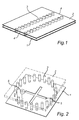
- a PGA rectangular waveguide In a first embodiment, as illustrated in Fig. 1 , an example of a PGA rectangular waveguide is illustrated.
- the waveguide comprises a first conducting layer 1, and a second conducting layer 2 (here made semitransparent, for increased visibility).
- the conducting layers are arranged at a constant distance h from each other, thereby forming a gap there between.
- This waveguide resembles a conventional SIW with metallized via holes in a PCB with metal layer (ground) on both sides, upper (top) and lower (bottom) ground plane.
- metal layer ground
- the metalized via holes are replaced with a PGA, forming protruding elements 3 extending from, and fixedly connected to, the first conducting layer.
- the second conducting layer 2 rest on the protruding elements 3, and is also connected to these, e.g. by means of soldering.
- the protruding elements 3 are made of conducting material, such as metal. They can also be made of metallized plastics or ceramics.
- a waveguide is here formed between the conducting elements, here extending between the first and second ports 4.
- Fig 2 illustrates a circular cavity of a PGA rectangular waveguide. This is realized in a similar way as in the above-discussed straight waveguide of Fig. 1 , and comprises first and second conducting layers 1, 2, arranged with a gap there between, and protruding PGA elements extending between the conducting layers, and connected to these layers.
- the protruding elements 3 are here arranged along a circular path, enclosing a circular cavity.
- a feeding arrangement 6 and a X-shaped radiating slot opening 5 is provided.
- This circular waveguide cavity functions in similar ways as circular SIW cavity.
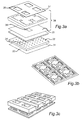
- Fig 3a shows the multilayer structure of a sub-assembly in an exploded view.
- the sub-assembly comprises a lower PCB 31 with a first ground plane/conducting layer 32, and a texture formed by protruding PGA elements 33 and a ridge structure 34, together forming PGA gap waveguide between the first ground place 32 and a second ground plane/conducting layer 35.
- the second ground plane 35 is here arranged on a second, upper PCB 36, which also comprises a third, upper ground plane/conducting layer 37.
- a gap is thus formed between both the first and second ground planes and between the second and third ground planes, respectively, thereby forming two layers of waveguides.
- Fig. 3a shows only a single subarray forming the unit cell (element) of a large array.
- Fig 3b shows an array of 4 such subarrays, arranged side-by-side in a rectangular configuration. There may be even larger arrays of such subarrays to form a more directive antenna.
- Fig 3c an alternative embodiment is shown, in which the upper conducting layer, including several sub-arrays, is formed as a continuous metal plate.
- This metal plate preferably has a thickness sufficient to allow grooves to be formed in it.
- elongate corrugations having similar effects as the slots in Fig 3b can instead be realized as elongate grooves extending between the unit cells.
- Either or both of the waveguide layers between the first and second conducting layer and the second and third conducting layer, respectively, may be made as a PGA waveguide or a PGA rectangular waveguide as discussed in the foregoing, without any substrate between the two metal ground planes, and with protruding PGA elements extending between the two conducting layers.
- the conventional via holes, as discussed in [13] will instead be metal pins or the like, which are manufactured as PGAs forming a PGA rectangular waveguide cavity or a PGA gap waveguide cavity between the two metal plates, within each unit cell of the whole antenna array.
- a top view of an example of the texture in the lower PCB of the antenna in Figure 3 is illustrated.
- This shows a distribution network 41 in ridge gap waveguide technology in accordance with [13], for waves in the gap between the two PCBs.
- the ridge structure forms a branched so-called corporate distribution network from one input port 42 to four output ports 43.
- the distribution network may be much larger than this with many more output ports to feed a larger array.
- the via-holes arranged to provide a stopping texture are here formed as protruding elements 44 formed by PGA and/or BGA, to form a PGA gap waveguide.
- protruding elements 44 formed by PGA and/or BGA
- the ridge structure is drawn as a thin metal strip, a microstrip, supported by pins.
- the strip 45 it is also feasible to replace the strip 45 with a ridge formed in a separate manufacture process such as by spark erosion, and mount this ridge on the lower metal plate during the same procedure when the PGA is mounted. Thereby the ridge becomes a solid ridge such as shown in the ridge gap waveguides in e.g. [4].
- the antenna comprises three layers, illustrated separately in an exploded view.
- the upper layer 51 (left) comprises an array of radiating horn elements 52 formed therein.
- the middle layer 53 is arranged at a distance from the upper layer 51, so that a gap towards the upper layer is provided.
- This middle layer 53 comprises a microstrip distribution network 54 arranged on a substrate having no ground plane. The waves propagate in the air gap between the upper and middle layer, and above the microstrip paths.
- a lower layer 55 (right) is arranged beneath and in contact with the middle layer 53.
- This lower layer comprises an array of protruding elements 56, such as metal pins, manufactured using PGA and/or BGA technology, on a conducting layer 57.
- the conducting layer may be formed as a separate metal layer or as a metal surface of an upper ground plane of a PCB.
- the protruding elements are connected to the conducting layer in such a way that metal contact between the bases of all protruding elements is ensured.
- this antenna functionally and structurally resembles the antenna disclosed in [12], said document hereby being incorporated in its entirety by reference.
- this known antenna was realized by milling to form an inverted microstrip gap waveguide network
- the present example provides a distribution network realized as a PGA inverted microstrip gap waveguide, which entails many advantages, as has been discussed thoroughly in the foregoing sections of this application.
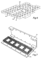
- Fig 6 provides a close-up view of an input port of a microstrip-ridge gap waveguide on a lower PCB showing a transition to a rectangular waveguide through a slot 63 in the ground plane.
- the conventionally used via holes are replaced by protruding PGA elements 61, connected to a conducting layer 62 in such a way that there is electric contact between all the protruding elements 61.
- a PGA microstrip gap waveguide is provided.
- the upper metal surface is removed for clarity.
- the microstrip supported by pins, i.e. the micrtostrip-ridge may also be replaced by a solid ridge in the same way as discussed above in connection with Fig 4 .
- Fig 7 illustrates an exemplary embodiment of a gap waveguide filter, structurally and functionally similar to the one disclosed in [14], said document hereby being incorporated in its entirety by reference.
- the protruding elements 71 arranged on a lower conducting layer 72 are here formed by PGA technology.
- An upper conducting layer 73 is arranged above the protruding elements, in the same way as disclosed in [12]. Thus, this then becomes a groove PGA gap waveguide filter.
- Fig 8 provides another example of a waveguide filter, which may also be referred to as gap-waveguide-packaged microstrip filter.
- This filter functionally and structurally resembles the filter disclosed in [15], said document hereby being incorporated in its entirety by reference.
- the filter contrary to the filter disclosed in [15], the filter here is packaged by a PGA surface, in which protruding elements 81 provided on a conducting layer 82 are realized as PGA.
- Two alternative lids, comprising different number and arrangement of the protruding elements 81 are illustrated.
- the integrated circuits are MMIC amplifier modules 91, arranged in a chain configuration on a lower plate 92, here realized as a PCB having an upper main substrate, provided with a lower ground plane 93.
- a lid is provided, formed by a conducting layer 95, e.g. made of aluminum or any other suitable metal.
- the lid may be connected to the lower plate 92 by means of a surrounding frame or the like.
- the lid is further provided with protruding elements 96, 97, protruding towards the lower plate 92.
- the protruding elements are preferably of different heights, so that the elements overlying the integrated circuits 91 are of a lower height, and the elements overlying areas laterally outside the integrated circuits are of a greater height.
- holes are formed in the surface presented by the protruding elements, in which the integrated circuits are inserted.
- the protruding elements are in electric contact with the upper layer 95, and electrically connected to each other by this layer.
- the protruding elements are preferably not in contact neither with the lower plate 92, nor the integrated circuit modules 91.
- the protruding elements are formed on the upper layer 95 by PGA technology.
- This packaging is consequently an example of using the PGA gap waveguide as a packaging technology, according to the present invention.
Landscapes
- Physics & Mathematics (AREA)
- Electromagnetism (AREA)
- Optics & Photonics (AREA)
- Engineering & Computer Science (AREA)
- Manufacturing & Machinery (AREA)
- Waveguide Aerials (AREA)
- Variable-Direction Aerials And Aerial Arrays (AREA)
Priority Applications (8)
| Application Number | Priority Date | Filing Date | Title |
|---|---|---|---|
| EP14173128.1A EP2945222A1 (fr) | 2014-05-14 | 2014-06-19 | Partie RF de four à micro-ondes ou d'ondes millimétriques utilisant des technologies de matrice de broches (PGA) et/ou de grille matricielle à billes (BGA) |
| PCT/EP2015/057842 WO2015172948A2 (fr) | 2014-05-14 | 2015-04-10 | Guides d'ondes et lignes de transmission dans des espaces entre des surfaces conductrices parallèles |
| US15/311,128 US10263310B2 (en) | 2014-05-14 | 2015-04-10 | Waveguides and transmission lines in gaps between parallel conducting surfaces |
| JP2016566244A JP6607869B2 (ja) | 2014-05-14 | 2015-04-10 | 平行導電面間の間隙に設けられる導波路及び伝送線路 |
| CN201580024099.1A CN106537682B (zh) | 2014-05-14 | 2015-04-10 | 在平行导电平面之间的间隙中的波导和传输线 |
| ES15716030T ES2878029T3 (es) | 2014-05-14 | 2015-04-10 | Guías de ondas y líneas de transmisión en huecos entre superficies conductoras paralelas |
| BR112016026534A BR112016026534A2 (pt) | 2014-05-14 | 2015-04-10 | guias de onda e linhas de transmissão em vãos entre superfícies de condução paralelas |
| EP15716030.0A EP3143665B1 (fr) | 2014-05-14 | 2015-04-10 | Guides d'ondes et lignes de transmission dans des espaces entre des surfaces conductrices parallèles |
Applications Claiming Priority (2)
| Application Number | Priority Date | Filing Date | Title |
|---|---|---|---|
| EP14168282 | 2014-05-14 | ||
| EP14173128.1A EP2945222A1 (fr) | 2014-05-14 | 2014-06-19 | Partie RF de four à micro-ondes ou d'ondes millimétriques utilisant des technologies de matrice de broches (PGA) et/ou de grille matricielle à billes (BGA) |
Publications (1)
| Publication Number | Publication Date |
|---|---|
| EP2945222A1 true EP2945222A1 (fr) | 2015-11-18 |
Family
ID=50729368
Family Applications (1)
| Application Number | Title | Priority Date | Filing Date |
|---|---|---|---|
| EP14173128.1A Withdrawn EP2945222A1 (fr) | 2014-05-14 | 2014-06-19 | Partie RF de four à micro-ondes ou d'ondes millimétriques utilisant des technologies de matrice de broches (PGA) et/ou de grille matricielle à billes (BGA) |
Country Status (1)
| Country | Link |
|---|---|
| EP (1) | EP2945222A1 (fr) |
Cited By (45)
| Publication number | Priority date | Publication date | Assignee | Title |
|---|---|---|---|---|
| CN104733816A (zh) * | 2015-03-30 | 2015-06-24 | 西安电子科技大学 | 一种基于间隙波导技术的带通滤波器 |
| CN106067590A (zh) * | 2016-07-29 | 2016-11-02 | 南京信息职业技术学院 | 一种双频全向基片集成波导螺旋缝隙天线 |
| JP2017121050A (ja) * | 2015-12-24 | 2017-07-06 | 日本電産エレシス株式会社 | スロットアレーアンテナ、ならびに当該スロットアレーアンテナを備えるレーダ、レーダシステム、および無線通信システム |
| CN107039719A (zh) * | 2017-04-18 | 2017-08-11 | 南京理工大学 | 一种叠层基片集成波导结构的多模双通带平衡滤波器 |
| WO2017158020A1 (fr) * | 2016-03-16 | 2017-09-21 | Huber+Suhner Ag | Structure d'adaptateur avec canaux de guide d'ondes |
| CN107745166A (zh) * | 2017-09-15 | 2018-03-02 | 西南电子技术研究所(中国电子科技集团公司第十研究所) | 相控阵有源天线阵面多层敷铜基板焊接方法 |
| JP2018078483A (ja) * | 2016-11-10 | 2018-05-17 | 国立大学法人東京工業大学 | スロットアレーアンテナ |
| CN108232390A (zh) * | 2017-12-22 | 2018-06-29 | 广东盛路通信科技股份有限公司 | 用于毫米波多波束天线矩阵的交叉器 |
| CN109041413A (zh) * | 2018-10-31 | 2018-12-18 | 中国工程物理研究院电子工程研究所 | 一种深度抑制超宽带同步开关噪声的电磁带隙结构 |
| CN109149036A (zh) * | 2018-08-03 | 2019-01-04 | 深圳鲲鹏无限科技有限公司 | 一种滤波器结构 |
| CN109196713A (zh) * | 2016-07-22 | 2019-01-11 | 株式会社藤仓 | 双工器及信号收发系统 |
| WO2019051601A1 (fr) * | 2017-09-15 | 2019-03-21 | Allen-Vanguard Corporation | Module frontal |
| CN109935965A (zh) * | 2019-04-10 | 2019-06-25 | 云南大学 | 集成基片间隙波导超宽带天线 |
| CN109980363A (zh) * | 2017-12-28 | 2019-07-05 | 华为技术有限公司 | 基于基片集成波导的阵列天线 |
| CN110061337A (zh) * | 2019-05-06 | 2019-07-26 | 云南大学 | 基于封装型集成基片间隙波导的定向耦合器 |
| RU2696676C1 (ru) * | 2018-12-06 | 2019-08-05 | Самсунг Электроникс Ко., Лтд. | Гребневый волновод без боковых стенок на базе печатной платы и содержащая его многослойная антенная решетка |
| CN110112522A (zh) * | 2019-05-31 | 2019-08-09 | 河南思维轨道交通技术研究院有限公司 | 一种基于缝隙波导技术的堆叠式高q双模滤波器 |
| CN110518321A (zh) * | 2019-09-02 | 2019-11-29 | 东南大学 | 一种基片集成波导水平过渡空气矩形波导的转接结构 |
| CN110571508A (zh) * | 2019-08-01 | 2019-12-13 | 中国电子科技集团公司第二十九研究所 | 一种宽带集成天线 |
| US10582608B2 (en) | 2016-07-20 | 2020-03-03 | Hcl Technologies Limited | Interconnection between printed circuit boards |
| CN111066201A (zh) * | 2017-09-25 | 2020-04-24 | 加普韦夫斯公司 | 相控阵天线 |
| CN111293439A (zh) * | 2019-12-30 | 2020-06-16 | 扬州船用电子仪器研究所(中国船舶重工集团公司第七二三研究所) | 一种毫米波低副瓣波导缝隙阵列天线 |
| DE102019200902A1 (de) | 2019-01-24 | 2020-07-30 | Audi Ag | Radarsensor, Kraftfahrzeug und Verfahren zum Herstellen eines Radarsensors |
| CN111585049A (zh) * | 2020-05-18 | 2020-08-25 | 宁波大学 | 一种低副瓣平板阵列天线 |
| CN111755810A (zh) * | 2019-03-27 | 2020-10-09 | 北京小米移动软件有限公司 | 天线模组、终端及天线模组的制作方法 |
| CN112290180A (zh) * | 2020-11-06 | 2021-01-29 | 上海交通大学 | 一种脊半模基片集成波导传输线 |
| CN112436295A (zh) * | 2021-01-28 | 2021-03-02 | 南京理工大学 | 基于脊间隙波导的毫米波高增益高辐射效率槽天线阵列 |
| CN112542692A (zh) * | 2020-11-19 | 2021-03-23 | Oppo广东移动通信有限公司 | 电子设备 |
| CN112563702A (zh) * | 2020-11-17 | 2021-03-26 | 杭州电子科技大学 | 基于hmsiw腔体的小型化双模滤波器及零点调节方法 |
| CN113097680A (zh) * | 2021-03-12 | 2021-07-09 | 南京理工大学 | 一种径向基片集成波导滤波功分器 |
| CN113454848A (zh) * | 2019-02-08 | 2021-09-28 | 加普韦夫斯公司 | 基于一种或多种超材料结构的天线阵列 |
| CN113659325A (zh) * | 2021-08-03 | 2021-11-16 | 超讯通信股份有限公司 | 集成基片间隙波导阵列天线 |
| US11201414B2 (en) | 2018-12-18 | 2021-12-14 | Veoneer Us, Inc. | Waveguide sensor assemblies and related methods |
| WO2021248392A1 (fr) * | 2020-06-08 | 2021-12-16 | 南京邮电大学 | Filtre passe-bande à bande ka d'ordre 4 basé sur un guide d'ondes à fente d'arête imprimée |
| CN113964512A (zh) * | 2021-10-22 | 2022-01-21 | 云南大学 | 一种三频集成基片间隙波导腔体滤波天线 |
| CN114267951A (zh) * | 2021-12-24 | 2022-04-01 | 中国航天科工集团八五一一研究所 | 一种宽带开口波导辐射天线及其设计方法 |
| CN114865262A (zh) * | 2021-02-04 | 2022-08-05 | 广州程星通信科技有限公司 | 基于电磁禁带结构的行波功率合成器 |
| CN114883808A (zh) * | 2022-05-23 | 2022-08-09 | 电子科技大学 | 一种基于siw的单层三通带频率选择表面 |
| CN115020953A (zh) * | 2022-06-14 | 2022-09-06 | 华南理工大学 | 基于微带脊间隙波导的毫米波背靠背层间过渡转换结构 |
| US20220368011A1 (en) * | 2021-05-17 | 2022-11-17 | HJWAVE Co., Ltd. | Multi-layer antenna structure supporting wide band and wide angle |
| CN116154439A (zh) * | 2022-11-16 | 2023-05-23 | 南京航空航天大学 | 全空气填充基片集成脊间隙波导及微带至矩形波导的过渡转换装置 |
| US11670829B2 (en) | 2017-02-08 | 2023-06-06 | Aptiv Technologies Limited. | Radar assembly with rectangular waveguide to substrate integrated waveguide transition |
| US11757166B2 (en) | 2020-11-10 | 2023-09-12 | Aptiv Technologies Limited | Surface-mount waveguide for vertical transitions of a printed circuit board |
| US11914067B2 (en) | 2021-04-29 | 2024-02-27 | Veoneer Us, Llc | Platformed post arrays for waveguides and related sensor assemblies |
| US11962087B2 (en) | 2021-03-22 | 2024-04-16 | Aptiv Technologies AG | Radar antenna system comprising an air waveguide antenna having a single layer material with air channels therein which is interfaced with a circuit board |
Citations (7)
| Publication number | Priority date | Publication date | Assignee | Title |
|---|---|---|---|---|
| US6194669B1 (en) * | 1999-02-05 | 2001-02-27 | Trw Inc. | Solder ball grid array for connecting multiple millimeter wave assemblies |
| US20110018657A1 (en) * | 2008-03-18 | 2011-01-27 | Shi Cheng | Substrate Integrated Waveguide |
| US20110210431A1 (en) * | 2010-01-27 | 2011-09-01 | Thales Holdings Uk Plc | Microwave circuit package |
| US20110285606A1 (en) * | 2008-11-19 | 2011-11-24 | Nxp B.V. | Millimetre-wave radio antenna module |
| EP2390953A1 (fr) * | 2010-05-25 | 2011-11-30 | Kildal Antenn Consulting AB | Conditionnement de circuits actifs et passifs de micro-ondes utilisant un couvercle ou un lit de poteaux recourbés |
| GB2499792A (en) * | 2012-02-28 | 2013-09-04 | Canon Kk | Electronic device comprising an electronic die, a substrate integrated waveguide (SIW) and a flip-chip ball grid array package |
| US20140111392A1 (en) * | 2011-11-29 | 2014-04-24 | Huawei Technologies Co., Ltd | Planar Waveguide, Waveguide Filter, and Antenna |
-
2014
- 2014-06-19 EP EP14173128.1A patent/EP2945222A1/fr not_active Withdrawn
Patent Citations (7)
| Publication number | Priority date | Publication date | Assignee | Title |
|---|---|---|---|---|
| US6194669B1 (en) * | 1999-02-05 | 2001-02-27 | Trw Inc. | Solder ball grid array for connecting multiple millimeter wave assemblies |
| US20110018657A1 (en) * | 2008-03-18 | 2011-01-27 | Shi Cheng | Substrate Integrated Waveguide |
| US20110285606A1 (en) * | 2008-11-19 | 2011-11-24 | Nxp B.V. | Millimetre-wave radio antenna module |
| US20110210431A1 (en) * | 2010-01-27 | 2011-09-01 | Thales Holdings Uk Plc | Microwave circuit package |
| EP2390953A1 (fr) * | 2010-05-25 | 2011-11-30 | Kildal Antenn Consulting AB | Conditionnement de circuits actifs et passifs de micro-ondes utilisant un couvercle ou un lit de poteaux recourbés |
| US20140111392A1 (en) * | 2011-11-29 | 2014-04-24 | Huawei Technologies Co., Ltd | Planar Waveguide, Waveguide Filter, and Antenna |
| GB2499792A (en) * | 2012-02-28 | 2013-09-04 | Canon Kk | Electronic device comprising an electronic die, a substrate integrated waveguide (SIW) and a flip-chip ball grid array package |
Non-Patent Citations (18)
| Title |
|---|
| A. ALGABA BRAZAIEZ; A. UZ ZAMAN; P.-S. KILDAL: "Improved Microstrip Filters Using PMC Packaging by Lid of Nails", IEEE TRANSACTIONS ON COMPONENTS, PACKAGING AND MANUFACTURING TECHNOLOGY, vol. 2, no. 7, July 2012 (2012-07-01), XP055206928, DOI: doi:10.1109/TCPMT.2012.2190931 |
| A. U. ZAMAN; A. KISHK; P.-S. KILDAL: "Narrow-band microwave filter using high Q groove gap waveguide resonators without sidewalls", IEEE TRANSACTIONS ON COMPONENTS, PACKAGING AND MANUFACTURING TECHNOLOGY, vol. 2, no. 11, November 2012 (2012-11-01), pages 1882 - 1889 |
| A. VALERO-NOGUEIRA; J. DOMENECH; M. BAQUERO; J. . HERRANZ; E. ALFONSO; A. VILA: "Gap waveguides using a suspended strip on a bed of nails", IEEE ANTENNAS AND WIRELESS PROPAG. LETTERS, vol. 10, 2011, pages 1006 - 1009, XP011403072, DOI: doi:10.1109/LAWP.2011.2167591 |
| A.U. ZAMAN; T. VUKUSIC; M. ALEXANDERSON; P.-S. KILDAL: "Gap Waveguide PMC Packaging for Improved Isolation of Circuit Components in High Frequency Microwave Modules", IEEE TRANSACTIONS ON COMPONENTS, PACKAGING AND MANUFACTURING TECHNOLOGY, vol. 4, no. 1, 2014, pages 16 - 25, XP011536233, DOI: doi:10.1109/TCPMT.2013.2271651 |
| ASTRID ALGABA BRAZALEZ ET AL: "Improved Microstrip Filters Using PMC Packaging by Lid of Nails", IEEE TRANSACTIONS ON COMPONENTS, PACKAGING AND MANUFACTURING TECHNOLOGY, vol. 2, no. 7, 1 July 2012 (2012-07-01), pages 1075 - 1084, XP055206928, ISSN: 2156-3950, DOI: 10.1109/TCPMT.2012.2190931 * |
| E. PUCCI; A. U. ZAMAN; E. RAJO-IGLESIAS; P.-S. KILDAL: "New low loss inverted microstrip line using gap waveguide technology for slot antenna applications", 6TH EUROPEAN CONFERENCE ON ANTENNAS AND PROPAGATION EUCAP 2011, ROME, 11 April 2011 (2011-04-11) |
| E. PUCCI; E. RAJO-IGLESIAS; J.-L. VASQUUEZ-ROY; P.-S. KILDAL: "Planar Dual-Mode Horn Array with Corporate-Feed Network in Inverted Microstrip Gap Waveguide", IEEE TRANSACTIONS ON ANTENNAS AND PROPAGATION, March 2014 (2014-03-01) |
| E. PUCCI; E. RAJO-IGLESIAS; J.-L. VAZQUEZ-ROY; P.-S. KILDAL: "Design of a four-element horn antenna array fed by inverted microstrip gap waveguide", 2013 IEEE INTERNATIONAL SYMPOSIUM ON ANTENNAS AND PROPAGATION (IEEE AP-S 2013), ORLANDO, USA, 7 July 2013 (2013-07-07) |
| E. PUCCI; E. RAJO-IGLESIAS; P.-S. KILDAL: "New Microstrip Gap Waveguide on Mushroom-Type EBG for Packaging of Microwave Components", IEEE MICROWAVE AND WIRELESS COMPONENTS LETTERS, vol. 22, no. 3, March 2012 (2012-03-01), pages 129 - 131, XP011433789, DOI: doi:10.1109/LMWC.2011.2182638 |
| E. RAJO-IGLESIAS; P.-S. KILDAL: "Numerical studies of bandwidth of parallel plate cut-off realized by bed of nails, corrugations and mushroom-type EBG for use in gap waveguides", IET MICROWAVES, ANTENNAS & PROPAGATION, vol. 5, no. 3, March 2011 (2011-03-01), pages 282 - 289 |
| J. HIROKAWA; M. ANDO: "Efficiency of 76-GHz post-wall waveguide-fed parallel-plate slot arrays", IEEE TRANS. ANTENNA PROPAG., vol. 48, no. 11, November 2000 (2000-11-01), pages 1742 - 1745, XP001005160, DOI: doi:10.1109/8.900232 |
| P.-S. KILDAL: "Three metamaterial-based gap waveguides between parallel metal plates for mm/submm waves", 3RD EUROPEAN CONFERENCE ON ANTENNAS AND PROPAGATION, BERLIN, March 2009 (2009-03-01) |
| P.-S. KILDAL; A. UZ ZAMAN; E. RAJO-IGLESIAS; E. ALFONSO; A. VALERO-NOGUEIRA: "Design and experimental verification of ridge gap waveguides in bed of nails for parallel plate mode suppression", IET MICROWAVES, ANTENNAS & PROPAGATION, vol. 5, no. 3, March 2011 (2011-03-01), pages 262 - 270, XP006037907, DOI: doi:10.1049/IET-MAP:20100089 |
| P.-S. KILDAL; E. ALFONSO; A. VALERO-NOGUEIRA; E. RAJO-IGLESIAS: "Local metamaterial-based waveguides in gaps between parallel metal plates", IEEE ANTENNAS AND WIRELESS PROPAGATION LETTERS, vol. 8, 2009, pages 84 - 87, XP011330887, DOI: doi:10.1109/LAWP.2008.2011147 |
| PUCCI ELENA ET AL: "Design of a four-element horn antenna array fed by inverted microstrip gap waveguide", 2013 IEEE ANTENNAS AND PROPAGATION SOCIETY INTERNATIONAL SYMPOSIUM (APSURSI), IEEE, 7 July 2013 (2013-07-07), pages 1226 - 1227, XP032556690, ISSN: 1522-3965, ISBN: 978-1-4799-3538-3, [retrieved on 20140113], DOI: 10.1109/APS.2013.6711273 * |
| RAZAVI SEYED ALI ET AL: "Design of 60GHz planar array antennas using PCB-based microstrip-ridge gap waveguide and SIW", THE 8TH EUROPEAN CONFERENCE ON ANTENNAS AND PROPAGATION (EUCAP 2014), EUROPEAN ASSOCIATION ON ANTENNAS AND PROPAGATION, 6 April 2014 (2014-04-06), pages 1825 - 1828, XP032643143, DOI: 10.1109/EUCAP.2014.6902150 * |
| SEYED ALI RAZAVI; PER-SIMON KILDAL; LIANGLIANG XIANG; HAIGUANG CHEN; ESPERANZA ALFONSO: "Design of 60GHz Planar Array Antennas Using PCB-based Microstrip-Ridge Gap Waveguide and SIW", 8TH EUROPEAN CONFERENCE ON ANTENNAS AND PROPAGATION EUCAP 2014, THE HAGUE, THE NETHERLANDS, 6 April 2014 (2014-04-06) |
| ZAMAN ASHRAF UZ ET AL: "Gap Waveguide PMC Packaging for Improved Isolation of Circuit Components in High-Frequency Microwave Modules", IEEE TRANSACTIONS ON COMPONENTS, PACKAGING AND MANUFACTURING TECHNOLOGY, IEEE, USA, vol. 4, no. 1, 1 January 2014 (2014-01-01), pages 16 - 25, XP011536233, ISSN: 2156-3950, [retrieved on 20131231], DOI: 10.1109/TCPMT.2013.2271651 * |
Cited By (71)
| Publication number | Priority date | Publication date | Assignee | Title |
|---|---|---|---|---|
| CN104733816B (zh) * | 2015-03-30 | 2017-09-15 | 西安电子科技大学 | 一种基于间隙波导技术的带通滤波器 |
| CN104733816A (zh) * | 2015-03-30 | 2015-06-24 | 西安电子科技大学 | 一种基于间隙波导技术的带通滤波器 |
| JP2017121050A (ja) * | 2015-12-24 | 2017-07-06 | 日本電産エレシス株式会社 | スロットアレーアンテナ、ならびに当該スロットアレーアンテナを備えるレーダ、レーダシステム、および無線通信システム |
| US10957988B2 (en) | 2015-12-24 | 2021-03-23 | Nidec Corporation | Slot array antenna, and radar, radar system, and wireless communication system including the slot array antenna |
| US10658761B2 (en) | 2016-03-16 | 2020-05-19 | Huber+Suhner Ag | Adapter structure with waveguide channels |
| WO2017158020A1 (fr) * | 2016-03-16 | 2017-09-21 | Huber+Suhner Ag | Structure d'adaptateur avec canaux de guide d'ondes |
| US10582608B2 (en) | 2016-07-20 | 2020-03-03 | Hcl Technologies Limited | Interconnection between printed circuit boards |
| CN109196713A (zh) * | 2016-07-22 | 2019-01-11 | 株式会社藤仓 | 双工器及信号收发系统 |
| CN106067590B (zh) * | 2016-07-29 | 2018-11-13 | 南京信息职业技术学院 | 一种双频全向基片集成波导螺旋缝隙天线 |
| CN106067590A (zh) * | 2016-07-29 | 2016-11-02 | 南京信息职业技术学院 | 一种双频全向基片集成波导螺旋缝隙天线 |
| JP2018078483A (ja) * | 2016-11-10 | 2018-05-17 | 国立大学法人東京工業大学 | スロットアレーアンテナ |
| WO2018088106A1 (fr) * | 2016-11-10 | 2018-05-17 | 国立大学法人東京工業大学 | Antenne réseau à fentes |
| US11670829B2 (en) | 2017-02-08 | 2023-06-06 | Aptiv Technologies Limited. | Radar assembly with rectangular waveguide to substrate integrated waveguide transition |
| CN107039719A (zh) * | 2017-04-18 | 2017-08-11 | 南京理工大学 | 一种叠层基片集成波导结构的多模双通带平衡滤波器 |
| CN107039719B (zh) * | 2017-04-18 | 2019-04-16 | 南京理工大学 | 一种叠层基片集成波导结构的多模双通带平衡滤波器 |
| WO2019051601A1 (fr) * | 2017-09-15 | 2019-03-21 | Allen-Vanguard Corporation | Module frontal |
| CN107745166A (zh) * | 2017-09-15 | 2018-03-02 | 西南电子技术研究所(中国电子科技集团公司第十研究所) | 相控阵有源天线阵面多层敷铜基板焊接方法 |
| CN107745166B (zh) * | 2017-09-15 | 2022-07-08 | 西南电子技术研究所(中国电子科技集团公司第十研究所) | 相控阵有源天线阵面多层敷铜基板焊接方法 |
| CN111066201A (zh) * | 2017-09-25 | 2020-04-24 | 加普韦夫斯公司 | 相控阵天线 |
| CN108232390A (zh) * | 2017-12-22 | 2018-06-29 | 广东盛路通信科技股份有限公司 | 用于毫米波多波束天线矩阵的交叉器 |
| CN109980363A (zh) * | 2017-12-28 | 2019-07-05 | 华为技术有限公司 | 基于基片集成波导的阵列天线 |
| CN109980363B (zh) * | 2017-12-28 | 2020-12-15 | 华为技术有限公司 | 基于基片集成波导的阵列天线 |
| CN109149036A (zh) * | 2018-08-03 | 2019-01-04 | 深圳鲲鹏无限科技有限公司 | 一种滤波器结构 |
| CN109149036B (zh) * | 2018-08-03 | 2024-05-07 | 深圳鲲鹏无限科技有限公司 | 一种滤波器结构 |
| CN109041413A (zh) * | 2018-10-31 | 2018-12-18 | 中国工程物理研究院电子工程研究所 | 一种深度抑制超宽带同步开关噪声的电磁带隙结构 |
| US11626652B2 (en) | 2018-12-06 | 2023-04-11 | Samsung Electronics Co., Ltd | Ridge gap waveguide and multilayer antenna array including the same |
| CN113169457B (zh) * | 2018-12-06 | 2023-09-12 | 三星电子株式会社 | 脊间隙波导以及包括其的多层天线阵列 |
| RU2696676C1 (ru) * | 2018-12-06 | 2019-08-05 | Самсунг Электроникс Ко., Лтд. | Гребневый волновод без боковых стенок на базе печатной платы и содержащая его многослойная антенная решетка |
| CN113169457A (zh) * | 2018-12-06 | 2021-07-23 | 三星电子株式会社 | 脊间隙波导以及包括其的多层天线阵列 |
| US11201414B2 (en) | 2018-12-18 | 2021-12-14 | Veoneer Us, Inc. | Waveguide sensor assemblies and related methods |
| US11756903B2 (en) | 2019-01-24 | 2023-09-12 | Audi Ag | Radar sensor, motor vehicle and method for producing a radar sensor |
| DE102019200902A1 (de) | 2019-01-24 | 2020-07-30 | Audi Ag | Radarsensor, Kraftfahrzeug und Verfahren zum Herstellen eines Radarsensors |
| CN113454848A (zh) * | 2019-02-08 | 2021-09-28 | 加普韦夫斯公司 | 基于一种或多种超材料结构的天线阵列 |
| CN111755810A (zh) * | 2019-03-27 | 2020-10-09 | 北京小米移动软件有限公司 | 天线模组、终端及天线模组的制作方法 |
| CN109935965A (zh) * | 2019-04-10 | 2019-06-25 | 云南大学 | 集成基片间隙波导超宽带天线 |
| CN109935965B (zh) * | 2019-04-10 | 2024-01-26 | 云南大学 | 集成基片间隙波导超宽带天线 |
| CN110061337A (zh) * | 2019-05-06 | 2019-07-26 | 云南大学 | 基于封装型集成基片间隙波导的定向耦合器 |
| CN110061337B (zh) * | 2019-05-06 | 2023-10-27 | 云南大学 | 基于封装型集成基片间隙波导的定向耦合器 |
| CN110112522A (zh) * | 2019-05-31 | 2019-08-09 | 河南思维轨道交通技术研究院有限公司 | 一种基于缝隙波导技术的堆叠式高q双模滤波器 |
| CN110571508A (zh) * | 2019-08-01 | 2019-12-13 | 中国电子科技集团公司第二十九研究所 | 一种宽带集成天线 |
| CN110518321B (zh) * | 2019-09-02 | 2021-10-19 | 东南大学 | 一种基片集成波导水平过渡空气矩形波导的转接结构 |
| CN110518321A (zh) * | 2019-09-02 | 2019-11-29 | 东南大学 | 一种基片集成波导水平过渡空气矩形波导的转接结构 |
| CN111293439A (zh) * | 2019-12-30 | 2020-06-16 | 扬州船用电子仪器研究所(中国船舶重工集团公司第七二三研究所) | 一种毫米波低副瓣波导缝隙阵列天线 |
| CN111585049A (zh) * | 2020-05-18 | 2020-08-25 | 宁波大学 | 一种低副瓣平板阵列天线 |
| CN111585049B (zh) * | 2020-05-18 | 2021-04-16 | 宁波大学 | 一种低副瓣平板阵列天线 |
| WO2021248392A1 (fr) * | 2020-06-08 | 2021-12-16 | 南京邮电大学 | Filtre passe-bande à bande ka d'ordre 4 basé sur un guide d'ondes à fente d'arête imprimée |
| CN112290180A (zh) * | 2020-11-06 | 2021-01-29 | 上海交通大学 | 一种脊半模基片集成波导传输线 |
| US11757166B2 (en) | 2020-11-10 | 2023-09-12 | Aptiv Technologies Limited | Surface-mount waveguide for vertical transitions of a printed circuit board |
| CN112563702A (zh) * | 2020-11-17 | 2021-03-26 | 杭州电子科技大学 | 基于hmsiw腔体的小型化双模滤波器及零点调节方法 |
| CN112563702B (zh) * | 2020-11-17 | 2021-09-14 | 杭州电子科技大学 | 基于hmsiw腔体的小型化双模滤波器及零点调节方法 |
| CN112542692B (zh) * | 2020-11-19 | 2022-12-27 | Oppo广东移动通信有限公司 | 电子设备 |
| CN112542692A (zh) * | 2020-11-19 | 2021-03-23 | Oppo广东移动通信有限公司 | 电子设备 |
| CN112436295B (zh) * | 2021-01-28 | 2021-05-04 | 南京理工大学 | 基于脊间隙波导的毫米波高增益高辐射效率槽天线阵列 |
| CN112436295A (zh) * | 2021-01-28 | 2021-03-02 | 南京理工大学 | 基于脊间隙波导的毫米波高增益高辐射效率槽天线阵列 |
| CN114865262A (zh) * | 2021-02-04 | 2022-08-05 | 广州程星通信科技有限公司 | 基于电磁禁带结构的行波功率合成器 |
| CN114865262B (zh) * | 2021-02-04 | 2023-09-05 | 广州程星通信科技有限公司 | 基于电磁禁带结构的行波功率合成器 |
| CN113097680A (zh) * | 2021-03-12 | 2021-07-09 | 南京理工大学 | 一种径向基片集成波导滤波功分器 |
| US11962087B2 (en) | 2021-03-22 | 2024-04-16 | Aptiv Technologies AG | Radar antenna system comprising an air waveguide antenna having a single layer material with air channels therein which is interfaced with a circuit board |
| US11914067B2 (en) | 2021-04-29 | 2024-02-27 | Veoneer Us, Llc | Platformed post arrays for waveguides and related sensor assemblies |
| US20220368011A1 (en) * | 2021-05-17 | 2022-11-17 | HJWAVE Co., Ltd. | Multi-layer antenna structure supporting wide band and wide angle |
| US11749884B2 (en) * | 2021-05-17 | 2023-09-05 | HJWAVE Co., Ltd. | Multi-layer antenna structure supporting wide band and wide angle |
| CN113659325B (zh) * | 2021-08-03 | 2024-01-09 | 超讯通信股份有限公司 | 集成基片间隙波导阵列天线 |
| CN113659325A (zh) * | 2021-08-03 | 2021-11-16 | 超讯通信股份有限公司 | 集成基片间隙波导阵列天线 |
| CN113964512A (zh) * | 2021-10-22 | 2022-01-21 | 云南大学 | 一种三频集成基片间隙波导腔体滤波天线 |
| CN114267951A (zh) * | 2021-12-24 | 2022-04-01 | 中国航天科工集团八五一一研究所 | 一种宽带开口波导辐射天线及其设计方法 |
| CN114883808A (zh) * | 2022-05-23 | 2022-08-09 | 电子科技大学 | 一种基于siw的单层三通带频率选择表面 |
| CN114883808B (zh) * | 2022-05-23 | 2023-04-25 | 电子科技大学 | 一种基于siw的单层三通带频率选择表面 |
| CN115020953A (zh) * | 2022-06-14 | 2022-09-06 | 华南理工大学 | 基于微带脊间隙波导的毫米波背靠背层间过渡转换结构 |
| CN115020953B (zh) * | 2022-06-14 | 2022-12-16 | 华南理工大学 | 基于微带脊间隙波导的毫米波背靠背层间过渡转换结构 |
| CN116154439B (zh) * | 2022-11-16 | 2024-02-02 | 南京航空航天大学 | 全空气填充基片集成脊间隙波导及微带至矩形波导的过渡转换装置 |
| CN116154439A (zh) * | 2022-11-16 | 2023-05-23 | 南京航空航天大学 | 全空气填充基片集成脊间隙波导及微带至矩形波导的过渡转换装置 |
Similar Documents
| Publication | Publication Date | Title |
|---|---|---|
| EP2945222A1 (fr) | Partie RF de four à micro-ondes ou d'ondes millimétriques utilisant des technologies de matrice de broches (PGA) et/ou de grille matricielle à billes (BGA) | |
| US10498000B2 (en) | Microwave or millimeter wave RF part realized by die-forming | |
| EP3143665B1 (fr) | Guides d'ondes et lignes de transmission dans des espaces entre des surfaces conductrices parallèles | |
| JP7264884B2 (ja) | フェーズドアレイアンテナ | |
| US10892536B2 (en) | Waveguides and transmission lines in gaps between parallel conducting surfaces | |
| US20200168974A1 (en) | Transition arrangement, a transition structure, and an integrated packaged structure | |
| CN109742525B (zh) | 一种滤波天线 | |
| JP2004327641A (ja) | 電子部品モジュール | |
| WO2016058627A1 (fr) | Composant rf à micro-ondes ou ondes millimétriques assemblé avec la technologie du bras-transfert | |
| EP4362219A1 (fr) | Structure d'antenne et procédé de fabrication de structure d'antenne | |
| JP3976004B2 (ja) | T分岐導波管、およびアレーアンテナ | |
| CN116387825A (zh) | 一种耦合馈电全金属毫米波双极化滤波天线 |
Legal Events
| Date | Code | Title | Description |
|---|---|---|---|
| PUAI | Public reference made under article 153(3) epc to a published international application that has entered the european phase |
Free format text: ORIGINAL CODE: 0009012 |
|
| AK | Designated contracting states |
Kind code of ref document: A1 Designated state(s): AL AT BE BG CH CY CZ DE DK EE ES FI FR GB GR HR HU IE IS IT LI LT LU LV MC MK MT NL NO PL PT RO RS SE SI SK SM TR |
|
| AX | Request for extension of the european patent |
Extension state: BA ME |
|
| STAA | Information on the status of an ep patent application or granted ep patent |
Free format text: STATUS: THE APPLICATION IS DEEMED TO BE WITHDRAWN |
|
| 18D | Application deemed to be withdrawn |
Effective date: 20160519 |