EP3364457A1 - Conditionnement de circuit intégré avec antenne - Google Patents
Conditionnement de circuit intégré avec antenne Download PDFInfo
- Publication number
- EP3364457A1 EP3364457A1 EP17156367.9A EP17156367A EP3364457A1 EP 3364457 A1 EP3364457 A1 EP 3364457A1 EP 17156367 A EP17156367 A EP 17156367A EP 3364457 A1 EP3364457 A1 EP 3364457A1
- Authority
- EP
- European Patent Office
- Prior art keywords
- integrated circuit
- antenna
- circuit package
- package
- layer
- Prior art date
- Legal status (The legal status is an assumption and is not a legal conclusion. Google has not performed a legal analysis and makes no representation as to the accuracy of the status listed.)
- Withdrawn
Links
Images


Classifications
-
- H—ELECTRICITY
- H01—ELECTRIC ELEMENTS
- H01L—SEMICONDUCTOR DEVICES NOT COVERED BY CLASS H10
- H01L23/00—Details of semiconductor or other solid state devices
- H01L23/58—Structural electrical arrangements for semiconductor devices not otherwise provided for, e.g. in combination with batteries
- H01L23/64—Impedance arrangements
- H01L23/66—High-frequency adaptations
-
- H—ELECTRICITY
- H01—ELECTRIC ELEMENTS
- H01L—SEMICONDUCTOR DEVICES NOT COVERED BY CLASS H10
- H01L23/00—Details of semiconductor or other solid state devices
- H01L23/48—Arrangements for conducting electric current to or from the solid state body in operation, e.g. leads, terminal arrangements ; Selection of materials therefor
- H01L23/488—Arrangements for conducting electric current to or from the solid state body in operation, e.g. leads, terminal arrangements ; Selection of materials therefor consisting of soldered or bonded constructions
- H01L23/498—Leads, i.e. metallisations or lead-frames on insulating substrates, e.g. chip carriers
- H01L23/49811—Additional leads joined to the metallisation on the insulating substrate, e.g. pins, bumps, wires, flat leads
- H01L23/49816—Spherical bumps on the substrate for external connection, e.g. ball grid arrays [BGA]
-
- H—ELECTRICITY
- H01—ELECTRIC ELEMENTS
- H01L—SEMICONDUCTOR DEVICES NOT COVERED BY CLASS H10
- H01L23/00—Details of semiconductor or other solid state devices
- H01L23/48—Arrangements for conducting electric current to or from the solid state body in operation, e.g. leads, terminal arrangements ; Selection of materials therefor
- H01L23/488—Arrangements for conducting electric current to or from the solid state body in operation, e.g. leads, terminal arrangements ; Selection of materials therefor consisting of soldered or bonded constructions
- H01L23/498—Leads, i.e. metallisations or lead-frames on insulating substrates, e.g. chip carriers
- H01L23/49827—Via connections through the substrates, e.g. pins going through the substrate, coaxial cables
-
- H—ELECTRICITY
- H01—ELECTRIC ELEMENTS
- H01L—SEMICONDUCTOR DEVICES NOT COVERED BY CLASS H10
- H01L25/00—Assemblies consisting of a plurality of individual semiconductor or other solid state devices ; Multistep manufacturing processes thereof
- H01L25/03—Assemblies consisting of a plurality of individual semiconductor or other solid state devices ; Multistep manufacturing processes thereof all the devices being of a type provided for in the same subgroup of groups H01L27/00 - H01L33/00, or in a single subclass of H10K, H10N, e.g. assemblies of rectifier diodes
- H01L25/04—Assemblies consisting of a plurality of individual semiconductor or other solid state devices ; Multistep manufacturing processes thereof all the devices being of a type provided for in the same subgroup of groups H01L27/00 - H01L33/00, or in a single subclass of H10K, H10N, e.g. assemblies of rectifier diodes the devices not having separate containers
- H01L25/065—Assemblies consisting of a plurality of individual semiconductor or other solid state devices ; Multistep manufacturing processes thereof all the devices being of a type provided for in the same subgroup of groups H01L27/00 - H01L33/00, or in a single subclass of H10K, H10N, e.g. assemblies of rectifier diodes the devices not having separate containers the devices being of a type provided for in group H01L27/00
- H01L25/0657—Stacked arrangements of devices
-
- H—ELECTRICITY
- H01—ELECTRIC ELEMENTS
- H01Q—ANTENNAS, i.e. RADIO AERIALS
- H01Q1/00—Details of, or arrangements associated with, antennas
- H01Q1/12—Supports; Mounting means
- H01Q1/22—Supports; Mounting means by structural association with other equipment or articles
- H01Q1/2283—Supports; Mounting means by structural association with other equipment or articles mounted in or on the surface of a semiconductor substrate as a chip-type antenna or integrated with other components into an IC package
-
- H—ELECTRICITY
- H01—ELECTRIC ELEMENTS
- H01Q—ANTENNAS, i.e. RADIO AERIALS
- H01Q1/00—Details of, or arrangements associated with, antennas
- H01Q1/40—Radiating elements coated with or embedded in protective material
-
- H—ELECTRICITY
- H01—ELECTRIC ELEMENTS
- H01Q—ANTENNAS, i.e. RADIO AERIALS
- H01Q13/00—Waveguide horns or mouths; Slot antennas; Leaky-waveguide antennas; Equivalent structures causing radiation along the transmission path of a guided wave
- H01Q13/10—Resonant slot antennas
- H01Q13/16—Folded slot antennas
-
- H—ELECTRICITY
- H01—ELECTRIC ELEMENTS
- H01Q—ANTENNAS, i.e. RADIO AERIALS
- H01Q15/00—Devices for reflection, refraction, diffraction or polarisation of waves radiated from an antenna, e.g. quasi-optical devices
- H01Q15/02—Refracting or diffracting devices, e.g. lens, prism
- H01Q15/10—Refracting or diffracting devices, e.g. lens, prism comprising three-dimensional array of impedance discontinuities, e.g. holes in conductive surfaces or conductive discs forming artificial dielectric
-
- H—ELECTRICITY
- H01—ELECTRIC ELEMENTS
- H01Q—ANTENNAS, i.e. RADIO AERIALS
- H01Q19/00—Combinations of primary active antenna elements and units with secondary devices, e.g. with quasi-optical devices, for giving the antenna a desired directional characteristic
- H01Q19/06—Combinations of primary active antenna elements and units with secondary devices, e.g. with quasi-optical devices, for giving the antenna a desired directional characteristic using refracting or diffracting devices, e.g. lens
- H01Q19/09—Combinations of primary active antenna elements and units with secondary devices, e.g. with quasi-optical devices, for giving the antenna a desired directional characteristic using refracting or diffracting devices, e.g. lens wherein the primary active element is coated with or embedded in a dielectric or magnetic material
-
- H—ELECTRICITY
- H01—ELECTRIC ELEMENTS
- H01Q—ANTENNAS, i.e. RADIO AERIALS
- H01Q19/00—Combinations of primary active antenna elements and units with secondary devices, e.g. with quasi-optical devices, for giving the antenna a desired directional characteristic
- H01Q19/10—Combinations of primary active antenna elements and units with secondary devices, e.g. with quasi-optical devices, for giving the antenna a desired directional characteristic using reflecting surfaces
-
- H—ELECTRICITY
- H01—ELECTRIC ELEMENTS
- H01Q—ANTENNAS, i.e. RADIO AERIALS
- H01Q19/00—Combinations of primary active antenna elements and units with secondary devices, e.g. with quasi-optical devices, for giving the antenna a desired directional characteristic
- H01Q19/28—Combinations of primary active antenna elements and units with secondary devices, e.g. with quasi-optical devices, for giving the antenna a desired directional characteristic using a secondary device in the form of two or more substantially straight conductive elements
-
- H—ELECTRICITY
- H01—ELECTRIC ELEMENTS
- H01Q—ANTENNAS, i.e. RADIO AERIALS
- H01Q21/00—Antenna arrays or systems
- H01Q21/06—Arrays of individually energised antenna units similarly polarised and spaced apart
- H01Q21/061—Two dimensional planar arrays
- H01Q21/064—Two dimensional planar arrays using horn or slot aerials
-
- H—ELECTRICITY
- H01—ELECTRIC ELEMENTS
- H01L—SEMICONDUCTOR DEVICES NOT COVERED BY CLASS H10
- H01L2223/00—Details relating to semiconductor or other solid state devices covered by the group H01L23/00
- H01L2223/58—Structural electrical arrangements for semiconductor devices not otherwise provided for
- H01L2223/64—Impedance arrangements
- H01L2223/66—High-frequency adaptations
- H01L2223/6605—High-frequency electrical connections
- H01L2223/6627—Waveguides, e.g. microstrip line, strip line, coplanar line
-
- H—ELECTRICITY
- H01—ELECTRIC ELEMENTS
- H01L—SEMICONDUCTOR DEVICES NOT COVERED BY CLASS H10
- H01L2223/00—Details relating to semiconductor or other solid state devices covered by the group H01L23/00
- H01L2223/58—Structural electrical arrangements for semiconductor devices not otherwise provided for
- H01L2223/64—Impedance arrangements
- H01L2223/66—High-frequency adaptations
- H01L2223/6661—High-frequency adaptations for passive devices
- H01L2223/6677—High-frequency adaptations for passive devices for antenna, e.g. antenna included within housing of semiconductor device
-
- H—ELECTRICITY
- H01—ELECTRIC ELEMENTS
- H01L—SEMICONDUCTOR DEVICES NOT COVERED BY CLASS H10
- H01L2223/00—Details relating to semiconductor or other solid state devices covered by the group H01L23/00
- H01L2223/58—Structural electrical arrangements for semiconductor devices not otherwise provided for
- H01L2223/64—Impedance arrangements
- H01L2223/66—High-frequency adaptations
- H01L2223/6683—High-frequency adaptations for monolithic microwave integrated circuit [MMIC]
-
- H—ELECTRICITY
- H01—ELECTRIC ELEMENTS
- H01L—SEMICONDUCTOR DEVICES NOT COVERED BY CLASS H10
- H01L2224/00—Indexing scheme for arrangements for connecting or disconnecting semiconductor or solid-state bodies and methods related thereto as covered by H01L24/00
- H01L2224/01—Means for bonding being attached to, or being formed on, the surface to be connected, e.g. chip-to-package, die-attach, "first-level" interconnects; Manufacturing methods related thereto
- H01L2224/02—Bonding areas; Manufacturing methods related thereto
- H01L2224/04—Structure, shape, material or disposition of the bonding areas prior to the connecting process
- H01L2224/04105—Bonding areas formed on an encapsulation of the semiconductor or solid-state body, e.g. bonding areas on chip-scale packages
-
- H—ELECTRICITY
- H01—ELECTRIC ELEMENTS
- H01L—SEMICONDUCTOR DEVICES NOT COVERED BY CLASS H10
- H01L2224/00—Indexing scheme for arrangements for connecting or disconnecting semiconductor or solid-state bodies and methods related thereto as covered by H01L24/00
- H01L2224/01—Means for bonding being attached to, or being formed on, the surface to be connected, e.g. chip-to-package, die-attach, "first-level" interconnects; Manufacturing methods related thereto
- H01L2224/10—Bump connectors; Manufacturing methods related thereto
- H01L2224/12—Structure, shape, material or disposition of the bump connectors prior to the connecting process
- H01L2224/12105—Bump connectors formed on an encapsulation of the semiconductor or solid-state body, e.g. bumps on chip-scale packages
-
- H—ELECTRICITY
- H01—ELECTRIC ELEMENTS
- H01L—SEMICONDUCTOR DEVICES NOT COVERED BY CLASS H10
- H01L2224/00—Indexing scheme for arrangements for connecting or disconnecting semiconductor or solid-state bodies and methods related thereto as covered by H01L24/00
- H01L2224/01—Means for bonding being attached to, or being formed on, the surface to be connected, e.g. chip-to-package, die-attach, "first-level" interconnects; Manufacturing methods related thereto
- H01L2224/10—Bump connectors; Manufacturing methods related thereto
- H01L2224/15—Structure, shape, material or disposition of the bump connectors after the connecting process
- H01L2224/16—Structure, shape, material or disposition of the bump connectors after the connecting process of an individual bump connector
- H01L2224/161—Disposition
- H01L2224/16151—Disposition the bump connector connecting between a semiconductor or solid-state body and an item not being a semiconductor or solid-state body, e.g. chip-to-substrate, chip-to-passive
- H01L2224/16221—Disposition the bump connector connecting between a semiconductor or solid-state body and an item not being a semiconductor or solid-state body, e.g. chip-to-substrate, chip-to-passive the body and the item being stacked
- H01L2224/16225—Disposition the bump connector connecting between a semiconductor or solid-state body and an item not being a semiconductor or solid-state body, e.g. chip-to-substrate, chip-to-passive the body and the item being stacked the item being non-metallic, e.g. insulating substrate with or without metallisation
- H01L2224/16227—Disposition the bump connector connecting between a semiconductor or solid-state body and an item not being a semiconductor or solid-state body, e.g. chip-to-substrate, chip-to-passive the body and the item being stacked the item being non-metallic, e.g. insulating substrate with or without metallisation the bump connector connecting to a bond pad of the item
-
- H—ELECTRICITY
- H01—ELECTRIC ELEMENTS
- H01L—SEMICONDUCTOR DEVICES NOT COVERED BY CLASS H10
- H01L2224/00—Indexing scheme for arrangements for connecting or disconnecting semiconductor or solid-state bodies and methods related thereto as covered by H01L24/00
- H01L2224/01—Means for bonding being attached to, or being formed on, the surface to be connected, e.g. chip-to-package, die-attach, "first-level" interconnects; Manufacturing methods related thereto
- H01L2224/18—High density interconnect [HDI] connectors; Manufacturing methods related thereto
- H01L2224/23—Structure, shape, material or disposition of the high density interconnect connectors after the connecting process
- H01L2224/24—Structure, shape, material or disposition of the high density interconnect connectors after the connecting process of an individual high density interconnect connector
- H01L2224/241—Disposition
- H01L2224/24151—Connecting between a semiconductor or solid-state body and an item not being a semiconductor or solid-state body, e.g. chip-to-substrate, chip-to-passive
- H01L2224/24153—Connecting between a semiconductor or solid-state body and an item not being a semiconductor or solid-state body, e.g. chip-to-substrate, chip-to-passive the body and the item being arranged next to each other, e.g. on a common substrate
- H01L2224/24195—Connecting between a semiconductor or solid-state body and an item not being a semiconductor or solid-state body, e.g. chip-to-substrate, chip-to-passive the body and the item being arranged next to each other, e.g. on a common substrate the item being a discrete passive component
-
- H—ELECTRICITY
- H01—ELECTRIC ELEMENTS
- H01L—SEMICONDUCTOR DEVICES NOT COVERED BY CLASS H10
- H01L2224/00—Indexing scheme for arrangements for connecting or disconnecting semiconductor or solid-state bodies and methods related thereto as covered by H01L24/00
- H01L2224/01—Means for bonding being attached to, or being formed on, the surface to be connected, e.g. chip-to-package, die-attach, "first-level" interconnects; Manufacturing methods related thereto
- H01L2224/26—Layer connectors, e.g. plate connectors, solder or adhesive layers; Manufacturing methods related thereto
- H01L2224/31—Structure, shape, material or disposition of the layer connectors after the connecting process
- H01L2224/32—Structure, shape, material or disposition of the layer connectors after the connecting process of an individual layer connector
- H01L2224/321—Disposition
- H01L2224/32151—Disposition the layer connector connecting between a semiconductor or solid-state body and an item not being a semiconductor or solid-state body, e.g. chip-to-substrate, chip-to-passive
- H01L2224/32221—Disposition the layer connector connecting between a semiconductor or solid-state body and an item not being a semiconductor or solid-state body, e.g. chip-to-substrate, chip-to-passive the body and the item being stacked
- H01L2224/32225—Disposition the layer connector connecting between a semiconductor or solid-state body and an item not being a semiconductor or solid-state body, e.g. chip-to-substrate, chip-to-passive the body and the item being stacked the item being non-metallic, e.g. insulating substrate with or without metallisation
-
- H—ELECTRICITY
- H01—ELECTRIC ELEMENTS
- H01L—SEMICONDUCTOR DEVICES NOT COVERED BY CLASS H10
- H01L2224/00—Indexing scheme for arrangements for connecting or disconnecting semiconductor or solid-state bodies and methods related thereto as covered by H01L24/00
- H01L2224/73—Means for bonding being of different types provided for in two or more of groups H01L2224/10, H01L2224/18, H01L2224/26, H01L2224/34, H01L2224/42, H01L2224/50, H01L2224/63, H01L2224/71
- H01L2224/732—Location after the connecting process
- H01L2224/73201—Location after the connecting process on the same surface
- H01L2224/73203—Bump and layer connectors
- H01L2224/73204—Bump and layer connectors the bump connector being embedded into the layer connector
-
- H—ELECTRICITY
- H01—ELECTRIC ELEMENTS
- H01L—SEMICONDUCTOR DEVICES NOT COVERED BY CLASS H10
- H01L2224/00—Indexing scheme for arrangements for connecting or disconnecting semiconductor or solid-state bodies and methods related thereto as covered by H01L24/00
- H01L2224/91—Methods for connecting semiconductor or solid state bodies including different methods provided for in two or more of groups H01L2224/80 - H01L2224/90
- H01L2224/92—Specific sequence of method steps
- H01L2224/921—Connecting a surface with connectors of different types
- H01L2224/9212—Sequential connecting processes
- H01L2224/92122—Sequential connecting processes the first connecting process involving a bump connector
- H01L2224/92125—Sequential connecting processes the first connecting process involving a bump connector the second connecting process involving a layer connector
-
- H—ELECTRICITY
- H01—ELECTRIC ELEMENTS
- H01L—SEMICONDUCTOR DEVICES NOT COVERED BY CLASS H10
- H01L23/00—Details of semiconductor or other solid state devices
- H01L23/28—Encapsulations, e.g. encapsulating layers, coatings, e.g. for protection
- H01L23/31—Encapsulations, e.g. encapsulating layers, coatings, e.g. for protection characterised by the arrangement or shape
- H01L23/3107—Encapsulations, e.g. encapsulating layers, coatings, e.g. for protection characterised by the arrangement or shape the device being completely enclosed
- H01L23/3121—Encapsulations, e.g. encapsulating layers, coatings, e.g. for protection characterised by the arrangement or shape the device being completely enclosed a substrate forming part of the encapsulation
- H01L23/3128—Encapsulations, e.g. encapsulating layers, coatings, e.g. for protection characterised by the arrangement or shape the device being completely enclosed a substrate forming part of the encapsulation the substrate having spherical bumps for external connection
-
- H—ELECTRICITY
- H01—ELECTRIC ELEMENTS
- H01L—SEMICONDUCTOR DEVICES NOT COVERED BY CLASS H10
- H01L24/00—Arrangements for connecting or disconnecting semiconductor or solid-state bodies; Methods or apparatus related thereto
- H01L24/01—Means for bonding being attached to, or being formed on, the surface to be connected, e.g. chip-to-package, die-attach, "first-level" interconnects; Manufacturing methods related thereto
- H01L24/10—Bump connectors ; Manufacturing methods related thereto
- H01L24/15—Structure, shape, material or disposition of the bump connectors after the connecting process
- H01L24/16—Structure, shape, material or disposition of the bump connectors after the connecting process of an individual bump connector
-
- H—ELECTRICITY
- H01—ELECTRIC ELEMENTS
- H01L—SEMICONDUCTOR DEVICES NOT COVERED BY CLASS H10
- H01L24/00—Arrangements for connecting or disconnecting semiconductor or solid-state bodies; Methods or apparatus related thereto
- H01L24/01—Means for bonding being attached to, or being formed on, the surface to be connected, e.g. chip-to-package, die-attach, "first-level" interconnects; Manufacturing methods related thereto
- H01L24/18—High density interconnect [HDI] connectors; Manufacturing methods related thereto
- H01L24/20—Structure, shape, material or disposition of high density interconnect preforms
-
- H—ELECTRICITY
- H01—ELECTRIC ELEMENTS
- H01L—SEMICONDUCTOR DEVICES NOT COVERED BY CLASS H10
- H01L24/00—Arrangements for connecting or disconnecting semiconductor or solid-state bodies; Methods or apparatus related thereto
- H01L24/01—Means for bonding being attached to, or being formed on, the surface to be connected, e.g. chip-to-package, die-attach, "first-level" interconnects; Manufacturing methods related thereto
- H01L24/26—Layer connectors, e.g. plate connectors, solder or adhesive layers; Manufacturing methods related thereto
- H01L24/31—Structure, shape, material or disposition of the layer connectors after the connecting process
- H01L24/32—Structure, shape, material or disposition of the layer connectors after the connecting process of an individual layer connector
-
- H—ELECTRICITY
- H01—ELECTRIC ELEMENTS
- H01L—SEMICONDUCTOR DEVICES NOT COVERED BY CLASS H10
- H01L24/00—Arrangements for connecting or disconnecting semiconductor or solid-state bodies; Methods or apparatus related thereto
- H01L24/73—Means for bonding being of different types provided for in two or more of groups H01L24/10, H01L24/18, H01L24/26, H01L24/34, H01L24/42, H01L24/50, H01L24/63, H01L24/71
-
- H—ELECTRICITY
- H01—ELECTRIC ELEMENTS
- H01L—SEMICONDUCTOR DEVICES NOT COVERED BY CLASS H10
- H01L24/00—Arrangements for connecting or disconnecting semiconductor or solid-state bodies; Methods or apparatus related thereto
- H01L24/91—Methods for connecting semiconductor or solid state bodies including different methods provided for in two or more of groups H01L24/80 - H01L24/90
- H01L24/92—Specific sequence of method steps
-
- H—ELECTRICITY
- H01—ELECTRIC ELEMENTS
- H01L—SEMICONDUCTOR DEVICES NOT COVERED BY CLASS H10
- H01L2924/00—Indexing scheme for arrangements or methods for connecting or disconnecting semiconductor or solid-state bodies as covered by H01L24/00
- H01L2924/10—Details of semiconductor or other solid state devices to be connected
- H01L2924/102—Material of the semiconductor or solid state bodies
- H01L2924/1025—Semiconducting materials
- H01L2924/10251—Elemental semiconductors, i.e. Group IV
- H01L2924/10253—Silicon [Si]
-
- H—ELECTRICITY
- H01—ELECTRIC ELEMENTS
- H01L—SEMICONDUCTOR DEVICES NOT COVERED BY CLASS H10
- H01L2924/00—Indexing scheme for arrangements or methods for connecting or disconnecting semiconductor or solid-state bodies as covered by H01L24/00
- H01L2924/10—Details of semiconductor or other solid state devices to be connected
- H01L2924/102—Material of the semiconductor or solid state bodies
- H01L2924/1025—Semiconducting materials
- H01L2924/1026—Compound semiconductors
- H01L2924/1032—III-V
- H01L2924/10329—Gallium arsenide [GaAs]
-
- H—ELECTRICITY
- H01—ELECTRIC ELEMENTS
- H01L—SEMICONDUCTOR DEVICES NOT COVERED BY CLASS H10
- H01L2924/00—Indexing scheme for arrangements or methods for connecting or disconnecting semiconductor or solid-state bodies as covered by H01L24/00
- H01L2924/10—Details of semiconductor or other solid state devices to be connected
- H01L2924/11—Device type
- H01L2924/14—Integrated circuits
- H01L2924/141—Analog devices
- H01L2924/142—HF devices
- H01L2924/1421—RF devices
-
- H—ELECTRICITY
- H01—ELECTRIC ELEMENTS
- H01L—SEMICONDUCTOR DEVICES NOT COVERED BY CLASS H10
- H01L2924/00—Indexing scheme for arrangements or methods for connecting or disconnecting semiconductor or solid-state bodies as covered by H01L24/00
- H01L2924/10—Details of semiconductor or other solid state devices to be connected
- H01L2924/11—Device type
- H01L2924/14—Integrated circuits
- H01L2924/141—Analog devices
- H01L2924/1423—Monolithic Microwave Integrated Circuit [MMIC]
-
- H—ELECTRICITY
- H01—ELECTRIC ELEMENTS
- H01L—SEMICONDUCTOR DEVICES NOT COVERED BY CLASS H10
- H01L2924/00—Indexing scheme for arrangements or methods for connecting or disconnecting semiconductor or solid-state bodies as covered by H01L24/00
- H01L2924/15—Details of package parts other than the semiconductor or other solid state devices to be connected
- H01L2924/151—Die mounting substrate
- H01L2924/1517—Multilayer substrate
- H01L2924/15192—Resurf arrangement of the internal vias
-
- H—ELECTRICITY
- H01—ELECTRIC ELEMENTS
- H01L—SEMICONDUCTOR DEVICES NOT COVERED BY CLASS H10
- H01L2924/00—Indexing scheme for arrangements or methods for connecting or disconnecting semiconductor or solid-state bodies as covered by H01L24/00
- H01L2924/15—Details of package parts other than the semiconductor or other solid state devices to be connected
- H01L2924/151—Die mounting substrate
- H01L2924/153—Connection portion
- H01L2924/1531—Connection portion the connection portion being formed only on the surface of the substrate opposite to the die mounting surface
- H01L2924/15311—Connection portion the connection portion being formed only on the surface of the substrate opposite to the die mounting surface being a ball array, e.g. BGA
-
- H—ELECTRICITY
- H01—ELECTRIC ELEMENTS
- H01L—SEMICONDUCTOR DEVICES NOT COVERED BY CLASS H10
- H01L2924/00—Indexing scheme for arrangements or methods for connecting or disconnecting semiconductor or solid-state bodies as covered by H01L24/00
- H01L2924/15—Details of package parts other than the semiconductor or other solid state devices to be connected
- H01L2924/151—Die mounting substrate
- H01L2924/153—Connection portion
- H01L2924/1532—Connection portion the connection portion being formed on the die mounting surface of the substrate
- H01L2924/15321—Connection portion the connection portion being formed on the die mounting surface of the substrate being a ball array, e.g. BGA
-
- H—ELECTRICITY
- H01—ELECTRIC ELEMENTS
- H01L—SEMICONDUCTOR DEVICES NOT COVERED BY CLASS H10
- H01L2924/00—Indexing scheme for arrangements or methods for connecting or disconnecting semiconductor or solid-state bodies as covered by H01L24/00
- H01L2924/30—Technical effects
- H01L2924/301—Electrical effects
- H01L2924/30105—Capacitance
Definitions
- This disclosure relates to an integrated circuit package including an antenna.
- RF devices for millimeter-wave (mm-wave) applications such as car radar may include an antenna integrated in the integrated circuit package, which may also be referred to as an antenna-in-package.
- antenna-in-package At mm-wave frequencies, the RF-performance of the system is no longer determined only by the transceiver circuits and the antenna, but also strongly depends on the package and the interconnection between the transceiver and the antenna.
- An example package type used for antenna-in-package devices is a fan-out package for example the embedded wafer-level ball-grid-array (eWLB).
- the eWLB typically includes a mold compound surrounding the packaged semiconductor die or dice.
- the eWLB package may have one redistribution layer (RDL) on the same major surface of the package as the solder balls of the ball grid array (BGA). Some eWLB packages may have a second redistribution layer on the opposite major surface to the solder balls. Vias formed through the mold compound may be used to electrically connect the first and second redistribution layers.
- the opposite major surfaces of the eWLB package may also be referred to as the front-side and back-side of the package.
- Antenna-in-packages using the eWLB package concept may form a planar antenna in one of the redistribution layers.
- a reflector is typically implemented.
- this reflector uses the top layer metal of an external printed circuit board to which the package is soldered.
- the effectiveness of the reflector depends on the soldering process, since the height of solder balls defines the distance between the reflector and the antenna. A variation in this height can consequently affect the matching and insertion loss of the antenna.
- An alternative example in eWLB packages with two redistribution layers integrates a reflector into the package using the metal layer of one of the redistribution layers and integrates an antenna into the other redistribution layer.
- the antenna performance strongly depends on the mold thickness since at higher frequencies the surface wave loss can be very high which can deteriorate the far-field radiation pattern and the antenna gain in the desired direction. This surface wave loss may result in the antenna efficiency being reduced to 40% or lower.
- the antenna performance is affected by the package thickness that, in the eWLB package, is electrically thick in the mm-wave frequency range.
- the eWLB package itself supports propagation of guided waves (surface waves) that bounce within the package making the antenna performance very sensitive to the package dimensions.
- the antenna is in close proximity to the chip consisting mainly of material such as silicon or gallium-arsenide that has a high relative dielectric constant above 10. Consequently, a significant portion of the radiated power tends to couple with the integrated circuit die or chip rather than being radiated outside the package. This may result in asymmetric and degraded radiation patterns from the antenna.
- an integrated circuit package comprising: an integrated circuit die, an antenna structure coupled to the integrated circuit die and comprising a stacked arrangement of metal and dielectric layers, wherein a first metal layer includes a planar antenna and at least one further metal layer comprises an artificial dielectric layer.
- the antenna structure may comprise: a second metal layer including an antenna feed structure, the antenna feed structure being electrically connected to the integrated circuit die, wherein the planar antenna is configured to be electro-magnetically coupled to the antenna feed structure.
- the first metal layer may further comprise an antenna feed structure and the planar antenna may be configured to be electro-magnetically coupled to the antenna feed structure.
- the planar antenna may comprise at least two slots.
- the integrated circuit package may comprise an array of four planar antennas.
- the artificial dielectric layer may comprise a plurality of metal shapes arranged in a grid.
- the at least one further layer comprises a first further metal layer and a second further metal layer wherein each of the first and second further metal layers are at least partially patterned to form artificial dielectric layers.
- the antenna structure may comprise a multi-layer printed circuit board.
- the antenna structure and the integrated circuit die may be vertically stacked.
- the integrated circuit die may be a monolithic microwave integrated circuit.
- the integrated circuit package may comprise a first redistribution layer including a redistribution metal layer wherein the integrated circuit is electrically connected to the antenna structure via the redistribution metal layer.
- the redistribution metal layer may form part of the antenna structure.
- One or more embodiments of the integrated circuit package may further comprise a second redistribution layer wherein at least one artificial dielectric layer is formed in at least one of the first redistribution layer and the second redistribution layer.
- Embodiments of the integrated circuit package may be included in an embedded wafer level ball grid array package.
- Embodiments of the integrated circuit package may be included in a radar device for an automotive vehicle.
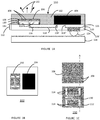
- FIG. 1A shows a cross-section of an integrated circuit package 100 implemented as an embedded wafer level BGA according to an embodiment.
- the integrated circuit package 100 includes an antenna structure 150 including a stacked arrangement of a first metal layer 108 and a second metal layer 112 separated by a dielectric layer 110.
- the antenna structure 150 may be implemented using a multilayer printed circuit board (PCB).
- the first metal layer 108 may be patterned to include a regular grid of metal squares 106.
- the second metal layer 112 may form a planar slot antenna 114 with a co-planar wave-guide feeder structure (not shown).
- the antenna structure 150 may transmit in direction 132.
- the integrated circuit package 100 also includes an integrated circuit die 104 that may implement for example a radio frequency (RF) transceiver.
- RF radio frequency
- the integrated circuit die 104 may be a monolithic microwave integrated circuit (MMIC).
- MMIC monolithic microwave integrated circuit
- the integrated circuit die 104 and the antenna 105 may be embedded in mold compound 102.
- a redistribution layer (RDL) 122 may be formed on one of the major surfaces of the mold compound 102. This process may be referred to as RDL last.
- the redistribution layer 122 may include a first dielectric layer 126, a redistribution metal layer 118, a second dielectric layer 126' and optionally an under-bump metallization (UBM) pad 120 onto which the solder balls 124 of the ball grid array may be attached.
- UBM under-bump metallization
- the BGA will typically have a number of pads and solder balls arranged in a grid which are then soldered to a printed circuit board 128 external to the integrated circuit package 100.
- One or more vias 116, 116', 116" may be formed in the first di-electric 126 on the redistribution layer 122 to electrically connect the integrated circuit die 104 to the pads 120 of the ball grid array.
- the integrated circuit die 104 may be electrically connected to the second metal layer 112 of the antenna structure with vias 116, 116' and the redistribution metal layer 118.
- Figure 1B shows a plan view of the integrated circuit package of figure 1A showing the relative arrangement of the antenna structure 150 and the die 104.
- the first metal layer 108 may be patterned to include a regular grid of metal squares 106.
- the metal squares 106 on the first metal layer 108 may be referred to as an artificial dielectric layer (ADL) or capacitive grid.
- ADL artificial dielectric layer
- the maximum dimension of each of the metal squares 106 must be less than a quarter of the wavelength of the dielectric hosting the artificial dielectric layer 106 of the transmitted wave to ensure that they are non-resonant.
- different metal shapes such as circles, hexagons, rectangles arranged periodically may also be used to form an ADL or capacitive grid.
- the inclusion of one or more ADLs 106 in the hosting dielectric 110 increases the effective permittivity, which may result in improved directionality of the antenna so that it transmits more of the energy in desired direction 132.
- a high relative permittivity >10
- the ADLs synthesize high relative permittivity (> 10) for radiation that travels normal to the metal layers, but low effective permittivity for radiation that travels parallel to the metal layers.
- the permittivity for radiation that travels parallel to the metal layers is determined by the relative permittivity of the hosting dielectric which is typically much lower, for example less than 5. This anisotropic behaviour may reduce the reflection at the top interface of the package and decrease the power lost into surface waves.
- the integrated circuit package 100 may reduce losses due to surface waves compared with known antenna-in-package solutions.
- the second metal layer 112 may form a planar slot antenna 114 with a co-planar wave-guide feeder structure 130.
- different planar antennas for example patch, dipole and loop antennas, may be used.
- different feeder structures for example single ended and differential feeder structures, H-slot coplanar waveguide feed, H-slot microstrip feed, Corporate feeding networks using either a coplanar waveguide feed or microstrip feed, or differential microstrip feeds may be implemented.
- feeder structure 130 and the planar slot antenna 114 can also be formed directly using redistribution metal layer 118. In this case via 116 and the second metal layer 112 may be omitted.
- the integrated circuit package 100 may result in improved antenna performance without the need for a reflector.
- a reflector typically requires a relatively large area, which may result in a larger package, and/or constraints on the metal routing required in either the redistribution layer 112 or the external printed circuit board 128.
- the antenna structure 150 does not require any vias between the metal layers 108 and 112. By reducing or eliminating the vias between the metal layers, the insertion loss at mm Wave frequencies may be reduced and the use of an additional matching circuit may be avoided. In addition, the cost and complexity of manufacturing an integrated circuit package including an antenna may be reduced.
- the integrated circuit package 100 may result in improved antenna-in-package performance with a reduced package size.
- the antenna structure 150 may be implemented as a printed circuit board, the distance between the layers can be more accurately controlled than for example the height of the solder balls 124 with respect to an external PCB 128. This may reduce the variation in performance of the antenna compared to antenna-in-package solutions that require an external reflector.
- the artificial dielectric layer 106 may be designed independently of the particular planar antenna and may be implemented so that it is above or overlaps the antenna. However, there is no requirement for fine alignment between the artificial dielectric layer and the planar antenna. This may allow implementation of the antenna structure 150 using standard printed circuit board thin-film manufacturing techniques.
- the integrated circuit package 100 may be implemented using an eWLB package. However, since the antenna structure 150 may be implemented as a multi-layer printed circuit board (PCB), it will be appreciated that other BGA packaging technologies may be used.
- the integrated circuit package 100 may implement a mm-wave transceiver device with an integrated antenna operating at frequencies above 120 GHz.
- the integrated circuit package may implement a transceiver for use in a car radar system operating at a frequency range of 76GHz to 81 GHz and in applications such as a parking aid, lateral collision avoidance, gesture recognition.
- the integrated circuit package 100 may implement a transceiver for use in multi-gigabit communication system which may operate at a frequency of 60 GHz.
- the integrated circuit package 100 may implement a transceiver operating at frequencies greater than 40 GHz.
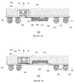
- FIG. 2A shows a cross-section of an integrated circuit package 200 implemented as an embedded wafer level BGA according to an embodiment.
- the integrated circuit package 200 includes an antenna structure 250 including a stacked arrangement of a first metal layer 208, a second metal layer 208', a third metal layer 212 and fourth metal layer 236.
- the metal layers 208,208', 212,236 are separated by dielectric layers 210, 210', 210".
- the first metal layer 208 may be patterned to include a regular grid of metal squares 206.
- the metal squares 206 patterned on the first metal layer 208 may be referred to as a first artificial dielectric layer (ADL).
- the second metal layer 208' may be patterned to include a regular grid of metal squares 206'.
- the metal squares 206' patterned on the second metal layer 208' may be referred to as a second artificial dielectric layer (ADL).
- the artificial dielectric layers 206, 206' may improve the gain of the antenna by enhancing the amount of radiation in a desired direction indicated by the arrows 232.
- the antenna structure 250 may be implemented using a multilayer printed circuit board.
- the integrated circuit package 200 also includes an integrated circuit die 204 which may implement for example a radio frequency (RF) transceiver.
- the integrated circuit die 204 may be a monolithic microwave integrated circuit (MMIC).
- MMIC monolithic microwave integrated circuit
- the integrated circuit die 204 and the antenna structure 250 may be embedded in a mold compound 202.
- An aperture 230 may be formed in the mold compound 202 so that a surface of the antenna structure 250 is exposed.
- a redistribution layer (RDL) 222 may be formed on the opposite surface of the mold compound 202 to the aperture 230.
- RDL redistribution layer
- the redistribution layer 222 may include a first dielectric layer 226, a redistribution metal layer 218, a second dielectric layer 226' and optionally an under-bump metallization (UBM) pad 220 onto which the solder balls 224 of the ball grid array may be attached.
- UBM under-bump metallization
- the integrated circuit package 200 has a number of pads and solder balls arranged in a grid which may be soldered to an external printed circuit board (not shown).
- One or more vias 216, 216', 216" may be formed in the first dielectric layer 226 for electrically connecting the integrated circuit die 204 to the pads 220 of the ball grid array and the antenna structure 250.
- Differential feeding lines 228 may be implemented in a fourth metal layer 236 of the antenna structure 250.
- the integrated circuit die 204 may be electrically connected to the differential feeding lines 228 with vias 216, 216' and the redistribution metal layer 218. Only one connection between the antenna structure 250 and the integrated circuit die 204 is shown explicitly.
- the third metal layer 212 may include a planar dual-slot antenna 214.
- the slots 214 may be dimensioned so that they are matched at a required resonant frequency.
- the slot length dimensions may be selected to be close to half wavelength long at 77 GHz. In this case the slot is tuned to a first resonance frequency. In other examples the length may be chosen with a dimension close to the wavelength to tune for the second resonance frequency. In general, the slot length is chosen dependent on the frequency or range of frequencies for which the antenna is to be tuned.
- the differential feeder structure may be electromagnetically coupled to the dual-slot antenna 214 in operation and so no vias are required between the third metal layer 212 and the fourth metal layer 236.
- different planar antennas and different feeder structures may be implemented.
- the differential feeder structure may be implemented using the redistribution metal layer 218.
- the redistribution layer 222 may be considered to form part of the antenna structure and the fourth metal layer 216 and dielectric layer 210" may be omitted.
- Figure 2B shows a plan view of the integrated circuit package of figure 2A showing the relative arrangement of the antenna structure 250 and the die 204.
- FIG. 2C shows a plan view of the metal layers of the antenna structure 250.
- the dashed line denoted B indicates the cross-section of the metal layers shown in figure 2A .
- the artificial dielectric formed by the first ADL 206, the dielectric layer 210 and the second ADL 206' typically increases the effective dielectric constant compared to the dielectric constant of the host material, i.e. the material forming the dielectric layers 210, 210' and 210". This increase in effective dielectric constant may improve the directionality of the antenna structure.
- the patterning on the first metal layer 208 and the second metal layer 208' may be aligned but can be misaligned within the normal tolerances of a multi-layer PCB manufacturing process.
- first and second artificial dielectric layers 206,206' may be misaligned by design. This may further increase the effective permittivity of the artificial dielectric.
- the patterning of the artificial dielectric layers 206, 206' on the first metal layer 208 and the second metal layer 208' may be identical.
- the ADLs 206,206' in the integrated circuit packages 200 form an equivalent dielectric medium due to two effects. Firstly, the capacitance of a ADL single layer or capacitive grid, which also is the case for integrated circuit package 100, and secondly the capacitance between the ADL layers 206, 206'.
- the equivalent dielectric medium formed by one or more ADL layers 206, 206' may result in improved the directionality of antenna gain in the desired direction.
- the integrated circuit package 200 may result in improved antenna performance without the need for a reflector.
- a reflector typically requires a relatively large area which may result in a larger package and/or constraints on the metal routing required in either the redistribution layers or the external printed circuit board.
- a reflector may impose constraints on the package for example requiring a clearance area on the package with no solder balls. Having fewer solder balls may reduce the mechanical strength of the package when soldered onto an external PCB, which may reduce the reliability of the circuit and/or package. By removing the requirement for a reflector, an electronic system including the integrated circuit package 200 may have improved reliability.
- the antenna structure 250 does not require any vias between any of the metal layers 208, 208', 212, and 236.
- the integrated circuit package 200 may result in improved antenna-in-package performance with a reduced package size. Since the antenna structure 250 may be implemented as a printed circuit board, the distance between the layers can be more accurately controlled than for example the height of the solder balls 224 with respect to an external printed-circuit board. The performance of the antenna structure 250 may be more predictable compared to antenna-in-package solutions that require an external reflector.
- the artificial dielectric layers may be designed independently of the particular planar antenna and although, the ADLs may be implemented above or overlapping the antenna, there is no requirement for fine alignment between the artificial dielectric layer and the antenna or between artificial dielectric layers. This allows implementation using standard printed circuit board thin-film manufacturing techniques.
- the integrated circuit package 200 may be implemented as an eWLB package.
- Figure 3A shows a flip chip BGA integrated circuit package 300 including an integrated antenna.
- the integrated circuit package 300 has a substrate 302 including a number of metal layers separated by dielectric layers (not shown).
- the substrate 302 is typically formed using a standard printed circuit board fabrication process.
- An antenna structure 250' similar to that described in figure 2 may be formed as a multi-layer printed circuit board and attached to the substrate 302.
- the antenna structure 250' may be over-molded by mold compound 304.
- a die 204' may be mounted on the same side of the substrate 302as the UBM pads 312 which have solder balls 310 attached. In other examples, the die 204' may be mounted on the opposite side of the substrate 302.
- the die 204' may be electrically connected to the UBM pads with flip-chip bumps 308 connected to the redistribution metal layer used to form the UBM pads 312.
- An underfill adhesive 314 may be added between the die 204' and the multilayer substrate 304.
- the die 204' may be electrically connected to the antenna structure by metal connection 306 and via 318.
- the antenna structure 250' includes artificial dielectric layers as previously described for figure 2 . Since the antenna structure 250' may be implemented as a printed circuit board, the distance between the layers can be more accurately controlled than for example the height of the solder balls 310 with respect to an external printed-circuit board. The performance of the antenna structure 250' may be more predictable compared to antenna-in-package solutions that require an external reflector.
- antenna structure 250' may also be used instead of antenna structure 250'. As shown the antenna structure 250' is shown offset to the side of the die 204'. It will be appreciated that other arrangements of the die 204' and the antenna structure 250' are possible. In some examples the antenna structure 250' may be arranged directly above the die 204' in a vertical stack. In operation, the antenna structure 250' may preferentially transmit radiation in the direction 320' due to the artificial dielectric layers. It will be appreciated that the antenna structure 250' may preferentially receive RF signals from the opposite direction to direction 320'.
- Figure 3B shows an embedded die BGA integrated circuit package 350 including an integrated antenna.
- the integrated circuit package 350 has a first substrate 352 and a multi-layer substrate 352 including a number of metal layers 364 separated by dielectric layers 366 formed above the first substrate 352.
- the multi-layer substrate 354 is typically formed using a standard printed circuit board fabrication process.
- the die 204" is mounted on the substrate 352 and connected to UBM pads 362 with vias 358 formed in the substrate 352.
- the UBM pads 362 may have solder balls 360 attached.
- An antenna structure 250" similar to that described in figure 2 may be formed within the multi-layer substrate 354.
- the die 204" may be located within a cavity formed in the multi-layer substrate 354 and electrically connected to the antenna structure 250" by metal connection 356.
- the antenna structure 250" includes artificial dielectric layers as previously described for figure 2 , which may reduce antenna losses. Since the antenna structure 250" may be implemented as a printed circuit board formed in the multi-layer substrate 354, the distance between the layers can be more accurately controlled than, for example, the height of the solder balls 360 with respect to an external printed-circuit-board. The performance of the antenna structure 250" may be more predictable compared to antenna-in-package solutions that require an external reflector. It will be appreciated that other antenna structures described herein may also be used instead of antenna structure 250". In operation, the antenna structure 250" may preferentially transmit radiation in the direction 320 due to the artificial dielectric layers. In other examples, the antenna 250" may be formed using a separate printed circuit board similar to antenna 250. In this case, the antenna may be placed within a cavity in the multi-layer substrate 354.
- Figure 4A shows a cross-section of an integrated circuit package 400 implemented as an embedded wafer level BGA with a front-side redistribution layer 430 and a back-side redistribution layer 422 according to an embodiment.
- the back-side redistribution layer 422 may be formed on a first major surface of the mold compound 402.
- the back-side redistribution layer 422 may include a first dielectric layer 426, a redistribution metal layer 418, a second dielectric layer 426' and optionally an under-bump metallization (UBM) pad 420 onto which the solder balls 424 of the ball grid array may be attached.
- UBM under-bump metallization
- the front-side redistribution layer 430 may be formed on a second major surface of the mold compound 402.
- the front-side redistribution layer 430 may include a first dielectric layer 438, a redistribution metal layer 408, a second dielectric layer 438'.
- the integrated circuit package 400 may have an antenna structure 450 including a stacked arrangement of a first metal layer which may be the front-side redistribution metal layer 408, a second metal layer 408', a third metal layer 412 and fourth metal layer 436.
- the first metal layer 408 may be patterned to include a regular grid of metal squares 406.
- the second metal layer 408' may be patterned to include a regular grid of metal squares 406'.
- the first metal layer 408 and second metal layer 408' are separated by a dielectric 434 formed by the mold compound 402 which acts as a dielectric layer and the first dielectric layer 438 of the front-side redistribution layer 430.
- the second metal layer 408' and third metal layer 412 are separated by dielectric layer 410.
- the third metal layer 412 and fourth metal layer 436 are separated by dielectric layer 410'.
- the third metal layer 412 may include an array of four planar dual-slot antennas 414a-d.
- the second metal layer 408', third metal layer 412 and fourth metal layer 436 of the antenna structure 450 and dielectric layers 410,410' may be implemented as a multilayer printed circuit board.
- the antenna structure 450' may enhance the amount of radiation in a desired direction 432. It will also be appreciated that the antenna structure 450' may preferentially receive RF signals from the opposite direction to the desired transmission direction 432.
- the integrated circuit package 400 also includes an integrated circuit die 404 which may implement for example a radio frequency (RF) transceiver.
- the integrated circuit die 404 may be a monolithic microwave integrated circuit (MMIC).
- MMIC monolithic microwave integrated circuit
- the integrated circuit die 404 and at least part of the antenna structure 450 may be embedded in the mold compound 402.
- the eWLB package will typically have a number of pads and solder balls arranged in a grid which are then soldered to an external printed circuit board (not shown).
- One or more vias 416, 416', 416" may be formed in the first dielectric layer 426 of the back-side redistribution layer 422 to electrically connect the integrated circuit die 404 to the pads 420 of the ball grid array and the antenna structure 450.
- the integrated circuit die 404 may be electrically connected to the differential feeder structure 428a implemented in the fourth metal layer 436 of the antenna structure with vias 416, 416' and the redistribution metal layer 418.
- connections to the differential feeder structures 428b, 428c, 428d may be similarly formed.
- further vias and metal tracks in redistribution metal layer 418 may be used to make further electrical connections between the die 404 and the fourth metal layer 436 of the antenna structure 450.
- the first metal layer 408 may be patterned to include a regular grid of metal squares 406.
- the second metal layer 408' may be patterned to include a regular grid of metal squares 406'.
- the metal squares 406 on the first metal layer 408 and the metal squares 406' patterned on the second metal layer 408' may effectively act as first and second artificial dielectric layers (ADL).
- the patterning on the first metal layer 408 and the second metal layer 408' may be aligned but can be misaligned within the normal tolerances of a multi-layer PCB manufacturing process.
- the patterning on the first metal layer 408 and the second metal layer 408' may be identical.
- the first ADL 406, the second ADL 406', and a dielectric layer 434 between the first ADL 406 and the second ADL 406' may form an artificial dielectric.
- the dielectric layer 434 may be formed by a combination of a layer of the mold compound 402, and the first dielectric layer 438 of the front-side redistribution layer 430.
- An artificial dielectric typically increases the effective dielectric constant of the dielectric material, which may improve the gain of the antenna by enhancing the amount of radiation in a desired direction indicated by the arrows 432.
- the effective dielectric constant in the vertical plane may be preferentially increased with respect to other directions. The may further enhance the amount of radiation towards the desired direction indicated by the arrows 432 when the antennas structure is used for transmission.
- the selectivity of the antenna structure may be improved when the antennas in the antenna structure 450 are used for receiving.
- the third metal layer 412 may include an array of four planar dual-slot antennas 414a-d.
- the slots are dimensioned to be matched at a required resonant frequency. For example, for car radar applications, dimensions may be selected to be close to one wavelength long at 77 GHz. Typically, the slot length may be chosen to be equivalent to half a wavelength of the radiation in free space.
- the fourth metal layer 436 may include four corresponding differential feeder structures 428a-d including a differential transmission line.
- the differential feeder structures 428a-d are operably electromagnetically coupled to the respective dual-slot antenna 414a-d and so no vias are required between the third metal layer 412 and the fourth metal layer 416.
- Each of the antennas 414 a-d may be used for transmission and/or reception.
- the integrated circuit package 400 may result in improved antenna performance without the need for a reflector.
- the antenna structure 450 does not require any vias between any of the metal layers 408, 408', 412, and 416.
- the integrated circuit package 400 may result in improved antenna-in-package performance with a reduced package size. Since the antenna structure 450 may be implemented as a printed circuit board, the distance between the layers can be more accurately controlled than for example the height of the solder balls 424 with respect to an external printed-circuit board.
- the performance of the antenna structure 450 in integrated circuit package 400 may be more predictable compared to antenna-in-package solutions that require an external reflector implemented on a printed circuit board.
- the artificial dielectric layers 408,408' may be designed independently of the particular planar antenna and although is implemented so that it is above or overlaps the antenna, there is no requirement for fine alignment between the artificial dielectric layer and the antenna. This may allow implementation using standard printed circuit board thin-film manufacturing techniques.
- the integrated circuit package 400 may be implemented using an eWLB package technology or other packaging technologies that include redistribution layers.
- Figure 4C shows the integrated circuit package 400 in plan-view indicating the relative placement of the integrated circuit die 404 and the antenna structure 450.
- Figure 4D shows a plan view of an alternative integrated circuit package 400' including a different example arrangement of integrated circuit die 404 and antenna structure 450.
- Figure 5A shows the antenna design in the integrated circuit package 400 corresponding to layers 412, 410 and 416 indicating the X-axis 508, Y-axis 510 and the Z-axis 432.
- the direction of the arrow indicated by the Z-axis indicates the desired direction of propagation 432 of the radiation.
- the E-plane corresponds to the X-Z plane.
- the H-plane corresponds to the Y-Z plane.
- the radiation beam varies between an angle of - ⁇ to + ⁇ where 0 degrees is orthogonal to the plane of the antenna i.e. parallel to the Z axis 432.
- Figure 5B shows the radiation pattern in the E-plane 500 of the antenna design in the integrated circuit package 400 corresponding to layers 412, 410 and 416.
- the results show the response when scanning from -45 to 0 degrees. Identical and mirrored patterns may be achieved between 0 and +45 degrees. Larger scanning angles of greater than 45 degrees may be obtained with a larger array i.e. more than 4 antenna elements.
- the x-axis 502 shows the angle of the radiation (theta) in degrees between -90 and +90 degrees.
- the y-axis shows the gain ranging from -5 dB to +15 dB.
- the plot lines 506 shows the gain of the antenna at frequencies between 76 GHz and 81 GHz in 1 GHz increments indicating a respective peak gain for each frequency between approximately -22 degrees and zero degrees.
- Figure 5C shows a polar plot 520 of the antenna in the corresponding H-plane 510 for the same frequency range shown as lines 522 at angles of theta between 0 and 360 degrees.
- the peak radiation for the H-plane has a value theta of 0 degrees for all the frequencies in the range.
- the graphs of radiation pattern in the E-plane 500 and H-plane 520 represent the response of the antenna before integration into a package with the integrated circuit die 402.
- the E-plane response 506 shows that the antenna may scan up to 45 degrees.
- the H- plane response 522 shows a symmetric radiation pattern for the antenna in free space.
- Figure 5D shows another view of the integrated circuit package 400' showing the integrated circuit die 404, the antenna structure 450 indicating the X-axis 508, Y-axis 510 and the Z-axis 432.
- the direction of the arrow indicated by the Z-axis indicates the desired direction of propagation 432 of the radiation.
- the E-plane corresponds to the X-Z plane.
- the H-plane corresponds to the Y-Z plane.
- the radiation beam varies between an angle of - ⁇ to + ⁇ where 0 degrees is orthogonal to the plane of the antenna i.e. parallel to the Z axis 432.
- Figure 5E shows the polar plot 530 of the simulated H-plane response of the antenna structure integrated into the integrated circuit package 400 for frequencies between 76 GHz and 81 GHz.
- the plot lines 532 of the antenna array show a relatively small asymmetry due to the presence of the integrated circuit die 402 which indicates that surface wave losses have been reduced.
- the E-plane response typically does not change with the die included.
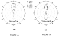
- ADLs in the hosting dielectric increases the effective permittivity, which may result in improved directionality of the antenna, as illustrated by figures 6A and 6B .
- a high relative permittivity >10
- the ADLs synthesize high relative permittivity (> 10) for radiation that travels normal to the metal layers, but low effective permittivity for radiation that travels parallel to the metal layers, since the permittivity in the latter direction is determined by the permittivity of the hosting dielectric which is typically much lower for example less than 5. This may reduce the reflection at the top interface of the package and decrease the power lost into surface waves.
- Figure 6A shows a polar plot 600 of the simulation of a radiation pattern in the E-plane for the antenna structure 450 for frequencies between 76 GHz and 81 GHz.
- Figure 6B shows a polar plot 610 of a simulation of the radiation of the antenna without the artificial dielectric layers for frequencies between 76 GHz and 81 GHz.
- the antenna design is identical and the material is identical i.e. the number of metal layers and dielectric layers of the PCB are the same.
- Plot 600 shows the antenna 450 has a unidirectional radiation pattern.
- Polar plot 610 shows the antenna that does not include ADLs radiates almost equal power in the up and down direction.
- the embodiments herein have been illustrated with the desired radiation antenna towards the opposite surface to the ball grid array.
- the antenna structure may be arranged such that the desired antenna radiation direction is toward the same surface is the ball grid array.
- one or more of the antenna structures described may be included in other package technologies than eWLB or BGA packages.
- the PCB may also be used to implement other interconnects for other components.
- Embodiments of the integrated circuit package may be used in mm-wave systems that use an antenna-in-package.
- the integrated circuit package may be used in 76-81 GHz car radar systems for multi-range (ultra-short, short, medium and long-range) applications such as a parking aid, lateral collision avoidance or other Advance driver assistance system (ADAS) applications and also for gesture recognition.
- the integrated circuit package may be used in mm-wave systems operating above 120GHz.
- the integrated circuit package may be used in the 60GHz range for multi-gigabit communications.
- An integrated circuit package comprising an integrated circuit die and an antenna structure coupled to the integrated circuit die and comprising a stacked arrangement of metal and dielectric layers, wherein a first metal layer includes a planar antenna and at least one further metal layer is at least partially patterned to form an artificial dielectric layer.
- the integrated circuit package may improve the directionality of the antenna and reduce the sensitivity of the antenna to the printed circuit board on which the integrated circuit package is mounted.
- the embodiments of the integrated circuit package may remove the requirement for a reflector on the printed circuit board.
- Embodiments of the integrated circuit package may allow for a thinner antenna-in-package which has reduced surface wave losses and an improved directionality of the antenna.
Priority Applications (3)
| Application Number | Priority Date | Filing Date | Title |
|---|---|---|---|
| EP17156367.9A EP3364457A1 (fr) | 2017-02-15 | 2017-02-15 | Conditionnement de circuit intégré avec antenne |
| US15/871,440 US10615134B2 (en) | 2017-02-15 | 2018-01-15 | Integrated circuit package |
| CN201810151190.5A CN108428693A (zh) | 2017-02-15 | 2018-02-13 | 集成电路封装 |
Applications Claiming Priority (1)
| Application Number | Priority Date | Filing Date | Title |
|---|---|---|---|
| EP17156367.9A EP3364457A1 (fr) | 2017-02-15 | 2017-02-15 | Conditionnement de circuit intégré avec antenne |
Publications (1)
| Publication Number | Publication Date |
|---|---|
| EP3364457A1 true EP3364457A1 (fr) | 2018-08-22 |
Family
ID=58054030
Family Applications (1)
| Application Number | Title | Priority Date | Filing Date |
|---|---|---|---|
| EP17156367.9A Withdrawn EP3364457A1 (fr) | 2017-02-15 | 2017-02-15 | Conditionnement de circuit intégré avec antenne |
Country Status (3)
| Country | Link |
|---|---|
| US (1) | US10615134B2 (fr) |
| EP (1) | EP3364457A1 (fr) |
| CN (1) | CN108428693A (fr) |
Cited By (6)
| Publication number | Priority date | Publication date | Assignee | Title |
|---|---|---|---|---|
| EP3474370A1 (fr) * | 2017-10-17 | 2019-04-24 | Mediatek Inc. | Antenne dans un boîtier ayant une structure de surface sélective en fréquence |
| FR3088479A1 (fr) * | 2018-11-14 | 2020-05-15 | Stmicroelectronics (Grenoble 2) Sas | Dispositif electronique incluant une puce electronique et une antenne |
| WO2020099531A1 (fr) * | 2018-11-15 | 2020-05-22 | Robert Bosch Gmbh | Ensemble circuit pour une antenne haute fréquence, procédé pour former un ensemble circuit, support de substrat et utilisation d'un ensemble circuit |
| DE102019102784A1 (de) * | 2019-02-05 | 2020-08-06 | Infineon Technologies Ag | Halbleitervorrichtungen mit Radar-Halbleiterchip und zugehörige Herstellungsverfahren |
| US10937748B1 (en) | 2019-09-12 | 2021-03-02 | Huawei Technologies Co., Ltd. | Fan-out transition structure for transmission of mm-Wave signals from IC to PCB via chip-scale packaging |
| US11784144B2 (en) | 2019-06-06 | 2023-10-10 | Infineon Technologies Ag | Semiconductor devices comprising planar waveguide transmission lines |
Families Citing this family (37)
| Publication number | Priority date | Publication date | Assignee | Title |
|---|---|---|---|---|
| US10468736B2 (en) | 2017-02-08 | 2019-11-05 | Aptiv Technologies Limited | Radar assembly with ultra wide band waveguide to substrate integrated waveguide transition |
| KR102352592B1 (ko) * | 2017-07-13 | 2022-01-19 | 삼성전자주식회사 | 어레이 안테나를 포함하는 전자 장치 |
| SG11202101034WA (en) * | 2018-08-02 | 2021-02-25 | Viasat Inc | Antenna element module |
| US10897076B2 (en) * | 2018-08-07 | 2021-01-19 | Veoneer Us, Inc. | Modular antenna systems for automotive radar sensors |
| US11271309B2 (en) | 2018-08-10 | 2022-03-08 | Ball Aerospace & Technologies Corp. | Systems and methods for interconnecting and isolating antenna system components |
| WO2020073329A1 (fr) * | 2018-10-12 | 2020-04-16 | 华为技术有限公司 | Antenne intégrée au boîtier à profil bas |
| US11011816B2 (en) * | 2018-10-29 | 2021-05-18 | Aptiv Technologies Limited | Radar assembly with a slot transition through a printed circuit board |
| DE102019200902A1 (de) * | 2019-01-24 | 2020-07-30 | Audi Ag | Radarsensor, Kraftfahrzeug und Verfahren zum Herstellen eines Radarsensors |
| KR102647754B1 (ko) * | 2019-04-16 | 2024-03-13 | 동우 화인켐 주식회사 | 안테나 패키지 및 이를 포함하는 화상 표시 장치 |
| WO2020220175A1 (fr) * | 2019-04-28 | 2020-11-05 | 加特兰微电子科技(上海)有限公司 | Antenne de boîtier et boîtier d'ensemble radar |
| US11527808B2 (en) * | 2019-04-29 | 2022-12-13 | Aptiv Technologies Limited | Waveguide launcher |
| US11380634B2 (en) | 2019-05-17 | 2022-07-05 | Nxp B.V. | Apparatuses and methods for coupling a waveguide structure to an integrated circuit package |
| KR20210009658A (ko) * | 2019-07-17 | 2021-01-27 | 동우 화인켐 주식회사 | 안테나 패키지 및 이를 포함하는 화상 표시 장치 |
| US11101540B2 (en) * | 2019-10-02 | 2021-08-24 | Amkor Technology Singapore Holding Pte. Ltd. | Semiconductor devices and methods of manufacturing semiconductor devices |
| CN113140887B (zh) * | 2020-01-17 | 2022-11-22 | 清华大学 | 封装天线及其制造方法 |
| EP3859891A1 (fr) | 2020-01-31 | 2021-08-04 | Nxp B.V. | Procédé et appareil comprenant un dispositif à semiconducteurs et appareil de test |
| EP3859892A1 (fr) | 2020-01-31 | 2021-08-04 | Nxp B.V. | Appareil de test et procédé de test d'un dispositif semiconducteurs |
| US11848499B2 (en) * | 2020-05-29 | 2023-12-19 | City University Of Hong Kong | On-chip antenna and on-chip antenna array |
| CN114063014A (zh) * | 2020-07-29 | 2022-02-18 | 华为技术有限公司 | 一种雷达装置和工作设备 |
| US11362436B2 (en) | 2020-10-02 | 2022-06-14 | Aptiv Technologies Limited | Plastic air-waveguide antenna with conductive particles |
| US11757166B2 (en) | 2020-11-10 | 2023-09-12 | Aptiv Technologies Limited | Surface-mount waveguide for vertical transitions of a printed circuit board |
| US11749883B2 (en) | 2020-12-18 | 2023-09-05 | Aptiv Technologies Limited | Waveguide with radiation slots and parasitic elements for asymmetrical coverage |
| US11901601B2 (en) | 2020-12-18 | 2024-02-13 | Aptiv Technologies Limited | Waveguide with a zigzag for suppressing grating lobes |
| US11502420B2 (en) | 2020-12-18 | 2022-11-15 | Aptiv Technologies Limited | Twin line fed dipole array antenna |
| US11681015B2 (en) | 2020-12-18 | 2023-06-20 | Aptiv Technologies Limited | Waveguide with squint alteration |
| US11626668B2 (en) | 2020-12-18 | 2023-04-11 | Aptiv Technologies Limited | Waveguide end array antenna to reduce grating lobes and cross-polarization |
| US11444364B2 (en) | 2020-12-22 | 2022-09-13 | Aptiv Technologies Limited | Folded waveguide for antenna |
| US11668787B2 (en) | 2021-01-29 | 2023-06-06 | Aptiv Technologies Limited | Waveguide with lobe suppression |
| US11721883B2 (en) * | 2021-02-25 | 2023-08-08 | Taiwan Semiconductor Manufacturing Company, Ltd. | Semiconductor package with antenna and method of forming the same |
| US11721905B2 (en) | 2021-03-16 | 2023-08-08 | Aptiv Technologies Limited | Waveguide with a beam-forming feature with radiation slots |
| US11616306B2 (en) | 2021-03-22 | 2023-03-28 | Aptiv Technologies Limited | Apparatus, method and system comprising an air waveguide antenna having a single layer material with air channels therein which is interfaced with a circuit board |
| US11973268B2 (en) | 2021-05-03 | 2024-04-30 | Aptiv Technologies AG | Multi-layered air waveguide antenna with layer-to-layer connections |
| US11962085B2 (en) | 2021-05-13 | 2024-04-16 | Aptiv Technologies AG | Two-part folded waveguide having a sinusoidal shape channel including horn shape radiating slots formed therein which are spaced apart by one-half wavelength |
| US11876059B2 (en) | 2021-05-17 | 2024-01-16 | Nxp Usa, Inc. | Semiconductor device with directing structure and method therefor |
| CN113410658B (zh) * | 2021-06-18 | 2022-12-02 | 安徽大学 | 一种毫米波高增益栅格缝隙阵列天线 |
| US11616282B2 (en) | 2021-08-03 | 2023-03-28 | Aptiv Technologies Limited | Transition between a single-ended port and differential ports having stubs that match with input impedances of the single-ended and differential ports |
| EP4343971A1 (fr) | 2022-09-26 | 2024-03-27 | Nxp B.V. | Unité d'antenne et procédé de production d'une unité d'antenne |
Citations (5)
| Publication number | Priority date | Publication date | Assignee | Title |
|---|---|---|---|---|
| EP2178119A1 (fr) * | 2008-10-20 | 2010-04-21 | Sibeam, Inc. | Schéma d'emballage de circuit intégré montable en surface |
| JP2010263413A (ja) * | 2009-05-07 | 2010-11-18 | Nippon Telegr & Teleph Corp <Ntt> | 高周波基板 |
| US20150061924A1 (en) * | 2012-02-29 | 2015-03-05 | Robert Bosch Gmbh | Semiconductor module having integrated antenna structures |
| US20150084830A1 (en) * | 2013-09-26 | 2015-03-26 | Adel Elsherbini | Antenna integrated in a package substrate |
| US20160006131A1 (en) * | 2014-07-04 | 2016-01-07 | Fujitsu Limited | High-frequency module and method for manufacturing the same |
Family Cites Families (10)
| Publication number | Priority date | Publication date | Assignee | Title |
|---|---|---|---|---|
| DE602005024587D1 (de) * | 2004-09-07 | 2010-12-16 | Nippon Telegraph & Telephone | Mehrschichtige Antennenvorrichtung mit vergrössertem Gewinn |
| US9196951B2 (en) * | 2012-11-26 | 2015-11-24 | International Business Machines Corporation | Millimeter-wave radio frequency integrated circuit packages with integrated antennas |
| JP5942273B2 (ja) * | 2013-01-29 | 2016-06-29 | パナソニックIpマネジメント株式会社 | 無線モジュール及び無線モジュールの製造方法 |
| US9461355B2 (en) * | 2013-03-29 | 2016-10-04 | Intel Corporation | Method apparatus and material for radio frequency passives and antennas |
| US9356332B2 (en) * | 2013-04-29 | 2016-05-31 | Infineon Technologies Ag | Integrated-circuit module with waveguide transition element |
| US9806422B2 (en) * | 2013-09-11 | 2017-10-31 | International Business Machines Corporation | Antenna-in-package structures with broadside and end-fire radiations |
| KR102185196B1 (ko) * | 2014-07-04 | 2020-12-01 | 삼성전자주식회사 | 무선 통신 기기에서 안테나 장치 |
| US9444135B2 (en) | 2014-09-19 | 2016-09-13 | Freescale Semiconductor, Inc. | Integrated circuit package |
| DE112017001710T5 (de) * | 2016-04-01 | 2018-12-20 | Sony Corporation | Mikrowellenantenneneinrichtung, Verpackungs- und Herstellungsverfahren |
| US10541464B2 (en) * | 2017-01-17 | 2020-01-21 | Sony Corporation | Microwave antenna coupling apparatus, microwave antenna apparatus and microwave antenna package |
-
2017
- 2017-02-15 EP EP17156367.9A patent/EP3364457A1/fr not_active Withdrawn
-
2018
- 2018-01-15 US US15/871,440 patent/US10615134B2/en active Active
- 2018-02-13 CN CN201810151190.5A patent/CN108428693A/zh active Pending
Patent Citations (5)
| Publication number | Priority date | Publication date | Assignee | Title |
|---|---|---|---|---|
| EP2178119A1 (fr) * | 2008-10-20 | 2010-04-21 | Sibeam, Inc. | Schéma d'emballage de circuit intégré montable en surface |
| JP2010263413A (ja) * | 2009-05-07 | 2010-11-18 | Nippon Telegr & Teleph Corp <Ntt> | 高周波基板 |
| US20150061924A1 (en) * | 2012-02-29 | 2015-03-05 | Robert Bosch Gmbh | Semiconductor module having integrated antenna structures |
| US20150084830A1 (en) * | 2013-09-26 | 2015-03-26 | Adel Elsherbini | Antenna integrated in a package substrate |
| US20160006131A1 (en) * | 2014-07-04 | 2016-01-07 | Fujitsu Limited | High-frequency module and method for manufacturing the same |
Cited By (10)
| Publication number | Priority date | Publication date | Assignee | Title |
|---|---|---|---|---|
| EP3474370A1 (fr) * | 2017-10-17 | 2019-04-24 | Mediatek Inc. | Antenne dans un boîtier ayant une structure de surface sélective en fréquence |
| US11322823B2 (en) | 2017-10-17 | 2022-05-03 | Mediatek Inc. | Antenna-in-package with frequency-selective surface structure |
| US11848481B2 (en) | 2017-10-17 | 2023-12-19 | Mediatek Inc. | Antenna-in-package with frequency-selective surface structure |
| FR3088479A1 (fr) * | 2018-11-14 | 2020-05-15 | Stmicroelectronics (Grenoble 2) Sas | Dispositif electronique incluant une puce electronique et une antenne |
| WO2020099531A1 (fr) * | 2018-11-15 | 2020-05-22 | Robert Bosch Gmbh | Ensemble circuit pour une antenne haute fréquence, procédé pour former un ensemble circuit, support de substrat et utilisation d'un ensemble circuit |
| DE102019102784A1 (de) * | 2019-02-05 | 2020-08-06 | Infineon Technologies Ag | Halbleitervorrichtungen mit Radar-Halbleiterchip und zugehörige Herstellungsverfahren |
| US11658135B2 (en) | 2019-02-05 | 2023-05-23 | Infineon Technologies Ag | Semiconductor devices comprising a radar semiconductor chip and associated production methods |
| US11784144B2 (en) | 2019-06-06 | 2023-10-10 | Infineon Technologies Ag | Semiconductor devices comprising planar waveguide transmission lines |
| US10937748B1 (en) | 2019-09-12 | 2021-03-02 | Huawei Technologies Co., Ltd. | Fan-out transition structure for transmission of mm-Wave signals from IC to PCB via chip-scale packaging |
| WO2021047667A1 (fr) * | 2019-09-12 | 2021-03-18 | Huawei Technologies Co., Ltd. | Structure de transition de sortance pour transmission de signaux à ondes millimétriques de circuit intégré à carte de circuit imprimé via boîtier-puce |
Also Published As
| Publication number | Publication date |
|---|---|
| US10615134B2 (en) | 2020-04-07 |
| CN108428693A (zh) | 2018-08-21 |
| US20180233465A1 (en) | 2018-08-16 |
Similar Documents
| Publication | Publication Date | Title |
|---|---|---|
| US10615134B2 (en) | Integrated circuit package | |
| US11658390B2 (en) | Wireless communications package with integrated antenna array | |
| US10431892B2 (en) | Antenna-in-package structures with broadside and end-fire radiations | |
| US10103450B2 (en) | Integration of area efficient antennas for phased array or wafer scale array antenna applications | |
| EP3547442B1 (fr) | Structure d'antenne avec élément de couplage intégré et boîtier de semiconducteur l'utilisant | |
| US8754818B2 (en) | Integrated antenna structure on separate semiconductor die | |
| US9985346B2 (en) | Wireless communications package with integrated antennas and air cavity | |
| US10109604B2 (en) | Package with embedded electronic components and a waveguide cavity through the package cover, antenna apparatus including package, and method of manufacturing the same | |
| US9819098B2 (en) | Antenna-in-package structures with broadside and end-fire radiations | |
| EP3065220B1 (fr) | Module à antenne intégrée et dispositif radar | |
| US9305888B2 (en) | Integrated antenna structure and array | |
| EP3032651A1 (fr) | Antenne de réseau à commande de phase d'émission et de réception commutables | |
| US9172131B2 (en) | Semiconductor structure having aperture antenna | |
| US20090015485A1 (en) | Method and Apparatus for Packaging an Integrated Chip and Antenna | |
| US11715886B2 (en) | Low-cost, IPD and laminate based antenna array module | |
| US11350522B2 (en) | Microwave antenna apparatus | |
| EP4362219A1 (fr) | Structure d'antenne et procédé de fabrication de structure d'antenne | |
| Kim et al. | Design of the 28 GHz Antenna-In-Package (AIP) Using Glass Embedded IC Technology |
Legal Events
| Date | Code | Title | Description |
|---|---|---|---|
| PUAI | Public reference made under article 153(3) epc to a published international application that has entered the european phase |
Free format text: ORIGINAL CODE: 0009012 |
|
| STAA | Information on the status of an ep patent application or granted ep patent |
Free format text: STATUS: THE APPLICATION HAS BEEN PUBLISHED |
|
| AK | Designated contracting states |
Kind code of ref document: A1 Designated state(s): AL AT BE BG CH CY CZ DE DK EE ES FI FR GB GR HR HU IE IS IT LI LT LU LV MC MK MT NL NO PL PT RO RS SE SI SK SM TR |
|
| AX | Request for extension of the european patent |
Extension state: BA ME |
|
| STAA | Information on the status of an ep patent application or granted ep patent |
Free format text: STATUS: REQUEST FOR EXAMINATION WAS MADE |
|
| 17P | Request for examination filed |
Effective date: 20190222 |
|
| RBV | Designated contracting states (corrected) |
Designated state(s): AL AT BE BG CH CY CZ DE DK EE ES FI FR GB GR HR HU IE IS IT LI LT LU LV MC MK MT NL NO PL PT RO RS SE SI SK SM TR |
|
| STAA | Information on the status of an ep patent application or granted ep patent |
Free format text: STATUS: REQUEST FOR EXAMINATION WAS MADE |
|
| STAA | Information on the status of an ep patent application or granted ep patent |
Free format text: STATUS: EXAMINATION IS IN PROGRESS |
|
| STAA | Information on the status of an ep patent application or granted ep patent |
Free format text: STATUS: EXAMINATION IS IN PROGRESS |
|
| 17Q | First examination report despatched |
Effective date: 20210216 |
|
| STAA | Information on the status of an ep patent application or granted ep patent |
Free format text: STATUS: THE APPLICATION IS DEEMED TO BE WITHDRAWN |
|
| 18D | Application deemed to be withdrawn |
Effective date: 20210827 |