EP3971963A1 - Halbleitergehäuseanordnung - Google Patents
Halbleitergehäuseanordnung Download PDFInfo
- Publication number
- EP3971963A1 EP3971963A1 EP21200916.1A EP21200916A EP3971963A1 EP 3971963 A1 EP3971963 A1 EP 3971963A1 EP 21200916 A EP21200916 A EP 21200916A EP 3971963 A1 EP3971963 A1 EP 3971963A1
- Authority
- EP
- European Patent Office
- Prior art keywords
- core substrate
- mask layer
- solder mask
- semiconductor package
- package assembly
- Prior art date
- Legal status (The legal status is an assumption and is not a legal conclusion. Google has not performed a legal analysis and makes no representation as to the accuracy of the status listed.)
- Granted
Links
Images


Classifications
-
- H—ELECTRICITY
- H10—SEMICONDUCTOR DEVICES; ELECTRIC SOLID-STATE DEVICES NOT OTHERWISE PROVIDED FOR
- H10W—GENERIC PACKAGES, INTERCONNECTIONS, CONNECTORS OR OTHER CONSTRUCTIONAL DETAILS OF DEVICES COVERED BY CLASS H10
- H10W74/00—Encapsulations, e.g. protective coatings
- H10W74/10—Encapsulations, e.g. protective coatings characterised by their shape or disposition
- H10W74/111—Encapsulations, e.g. protective coatings characterised by their shape or disposition the semiconductor body being completely enclosed
- H10W74/114—Encapsulations, e.g. protective coatings characterised by their shape or disposition the semiconductor body being completely enclosed by a substrate and the encapsulations
- H10W74/117—Encapsulations, e.g. protective coatings characterised by their shape or disposition the semiconductor body being completely enclosed by a substrate and the encapsulations the substrate having spherical bumps for external connection
-
- H—ELECTRICITY
- H10—SEMICONDUCTOR DEVICES; ELECTRIC SOLID-STATE DEVICES NOT OTHERWISE PROVIDED FOR
- H10W—GENERIC PACKAGES, INTERCONNECTIONS, CONNECTORS OR OTHER CONSTRUCTIONAL DETAILS OF DEVICES COVERED BY CLASS H10
- H10W70/00—Package substrates; Interposers; Redistribution layers [RDL]
- H10W70/60—Insulating or insulated package substrates; Interposers; Redistribution layers
- H10W70/62—Insulating or insulated package substrates; Interposers; Redistribution layers characterised by their interconnections
- H10W70/63—Vias, e.g. via plugs
- H10W70/635—Through-vias
-
- H—ELECTRICITY
- H10—SEMICONDUCTOR DEVICES; ELECTRIC SOLID-STATE DEVICES NOT OTHERWISE PROVIDED FOR
- H10W—GENERIC PACKAGES, INTERCONNECTIONS, CONNECTORS OR OTHER CONSTRUCTIONAL DETAILS OF DEVICES COVERED BY CLASS H10
- H10W70/00—Package substrates; Interposers; Redistribution layers [RDL]
- H10W70/60—Insulating or insulated package substrates; Interposers; Redistribution layers
- H10W70/67—Insulating or insulated package substrates; Interposers; Redistribution layers characterised by their insulating layers or insulating parts
- H10W70/69—Insulating materials thereof
- H10W70/695—Organic materials
-
- H—ELECTRICITY
- H10—SEMICONDUCTOR DEVICES; ELECTRIC SOLID-STATE DEVICES NOT OTHERWISE PROVIDED FOR
- H10W—GENERIC PACKAGES, INTERCONNECTIONS, CONNECTORS OR OTHER CONSTRUCTIONAL DETAILS OF DEVICES COVERED BY CLASS H10
- H10W20/00—Interconnections in chips, wafers or substrates
- H10W20/40—Interconnections external to wafers or substrates, e.g. back-end-of-line [BEOL] metallisations or vias connecting to gate electrodes
- H10W20/41—Interconnections external to wafers or substrates, e.g. back-end-of-line [BEOL] metallisations or vias connecting to gate electrodes characterised by their conductive parts
- H10W20/42—Vias, e.g. via plugs
-
- H—ELECTRICITY
- H10—SEMICONDUCTOR DEVICES; ELECTRIC SOLID-STATE DEVICES NOT OTHERWISE PROVIDED FOR
- H10W—GENERIC PACKAGES, INTERCONNECTIONS, CONNECTORS OR OTHER CONSTRUCTIONAL DETAILS OF DEVICES COVERED BY CLASS H10
- H10W70/00—Package substrates; Interposers; Redistribution layers [RDL]
- H10W70/40—Leadframes
- H10W70/464—Additional interconnections in combination with leadframes
- H10W70/465—Bumps or wires
-
- H—ELECTRICITY
- H10—SEMICONDUCTOR DEVICES; ELECTRIC SOLID-STATE DEVICES NOT OTHERWISE PROVIDED FOR
- H10W—GENERIC PACKAGES, INTERCONNECTIONS, CONNECTORS OR OTHER CONSTRUCTIONAL DETAILS OF DEVICES COVERED BY CLASS H10
- H10W70/00—Package substrates; Interposers; Redistribution layers [RDL]
- H10W70/60—Insulating or insulated package substrates; Interposers; Redistribution layers
- H10W70/67—Insulating or insulated package substrates; Interposers; Redistribution layers characterised by their insulating layers or insulating parts
- H10W70/69—Insulating materials thereof
-
- H—ELECTRICITY
- H10—SEMICONDUCTOR DEVICES; ELECTRIC SOLID-STATE DEVICES NOT OTHERWISE PROVIDED FOR
- H10W—GENERIC PACKAGES, INTERCONNECTIONS, CONNECTORS OR OTHER CONSTRUCTIONAL DETAILS OF DEVICES COVERED BY CLASS H10
- H10W72/00—Interconnections or connectors in packages
- H10W72/20—Bump connectors, e.g. solder bumps or copper pillars; Dummy bumps; Thermal bumps
-
- H—ELECTRICITY
- H10—SEMICONDUCTOR DEVICES; ELECTRIC SOLID-STATE DEVICES NOT OTHERWISE PROVIDED FOR
- H10W—GENERIC PACKAGES, INTERCONNECTIONS, CONNECTORS OR OTHER CONSTRUCTIONAL DETAILS OF DEVICES COVERED BY CLASS H10
- H10W72/00—Interconnections or connectors in packages
- H10W72/071—Connecting or disconnecting
- H10W72/072—Connecting or disconnecting of bump connectors
-
- H—ELECTRICITY
- H10—SEMICONDUCTOR DEVICES; ELECTRIC SOLID-STATE DEVICES NOT OTHERWISE PROVIDED FOR
- H10W—GENERIC PACKAGES, INTERCONNECTIONS, CONNECTORS OR OTHER CONSTRUCTIONAL DETAILS OF DEVICES COVERED BY CLASS H10
- H10W72/00—Interconnections or connectors in packages
- H10W72/071—Connecting or disconnecting
- H10W72/072—Connecting or disconnecting of bump connectors
- H10W72/07202—Connecting or disconnecting of bump connectors using auxiliary members
-
- H—ELECTRICITY
- H10—SEMICONDUCTOR DEVICES; ELECTRIC SOLID-STATE DEVICES NOT OTHERWISE PROVIDED FOR
- H10W—GENERIC PACKAGES, INTERCONNECTIONS, CONNECTORS OR OTHER CONSTRUCTIONAL DETAILS OF DEVICES COVERED BY CLASS H10
- H10W72/00—Interconnections or connectors in packages
- H10W72/071—Connecting or disconnecting
- H10W72/072—Connecting or disconnecting of bump connectors
- H10W72/07231—Techniques
- H10W72/07236—Soldering or alloying
-
- H—ELECTRICITY
- H10—SEMICONDUCTOR DEVICES; ELECTRIC SOLID-STATE DEVICES NOT OTHERWISE PROVIDED FOR
- H10W—GENERIC PACKAGES, INTERCONNECTIONS, CONNECTORS OR OTHER CONSTRUCTIONAL DETAILS OF DEVICES COVERED BY CLASS H10
- H10W72/00—Interconnections or connectors in packages
- H10W72/071—Connecting or disconnecting
- H10W72/073—Connecting or disconnecting of die-attach connectors
-
- H—ELECTRICITY
- H10—SEMICONDUCTOR DEVICES; ELECTRIC SOLID-STATE DEVICES NOT OTHERWISE PROVIDED FOR
- H10W—GENERIC PACKAGES, INTERCONNECTIONS, CONNECTORS OR OTHER CONSTRUCTIONAL DETAILS OF DEVICES COVERED BY CLASS H10
- H10W72/00—Interconnections or connectors in packages
- H10W72/20—Bump connectors, e.g. solder bumps or copper pillars; Dummy bumps; Thermal bumps
- H10W72/251—Materials
- H10W72/252—Materials comprising solid metals or solid metalloids, e.g. PbSn, Ag or Cu
-
- H—ELECTRICITY
- H10—SEMICONDUCTOR DEVICES; ELECTRIC SOLID-STATE DEVICES NOT OTHERWISE PROVIDED FOR
- H10W—GENERIC PACKAGES, INTERCONNECTIONS, CONNECTORS OR OTHER CONSTRUCTIONAL DETAILS OF DEVICES COVERED BY CLASS H10
- H10W72/00—Interconnections or connectors in packages
- H10W72/20—Bump connectors, e.g. solder bumps or copper pillars; Dummy bumps; Thermal bumps
- H10W72/29—Bond pads specially adapted therefor
-
- H—ELECTRICITY
- H10—SEMICONDUCTOR DEVICES; ELECTRIC SOLID-STATE DEVICES NOT OTHERWISE PROVIDED FOR
- H10W—GENERIC PACKAGES, INTERCONNECTIONS, CONNECTORS OR OTHER CONSTRUCTIONAL DETAILS OF DEVICES COVERED BY CLASS H10
- H10W72/00—Interconnections or connectors in packages
- H10W72/30—Die-attach connectors
- H10W72/321—Structures or relative sizes of die-attach connectors
- H10W72/325—Die-attach connectors having a filler embedded in a matrix
-
- H—ELECTRICITY
- H10—SEMICONDUCTOR DEVICES; ELECTRIC SOLID-STATE DEVICES NOT OTHERWISE PROVIDED FOR
- H10W—GENERIC PACKAGES, INTERCONNECTIONS, CONNECTORS OR OTHER CONSTRUCTIONAL DETAILS OF DEVICES COVERED BY CLASS H10
- H10W72/00—Interconnections or connectors in packages
- H10W72/30—Die-attach connectors
- H10W72/351—Materials of die-attach connectors
-
- H—ELECTRICITY
- H10—SEMICONDUCTOR DEVICES; ELECTRIC SOLID-STATE DEVICES NOT OTHERWISE PROVIDED FOR
- H10W—GENERIC PACKAGES, INTERCONNECTIONS, CONNECTORS OR OTHER CONSTRUCTIONAL DETAILS OF DEVICES COVERED BY CLASS H10
- H10W72/00—Interconnections or connectors in packages
- H10W72/30—Die-attach connectors
- H10W72/351—Materials of die-attach connectors
- H10W72/352—Materials of die-attach connectors comprising metals or metalloids, e.g. solders
-
- H—ELECTRICITY
- H10—SEMICONDUCTOR DEVICES; ELECTRIC SOLID-STATE DEVICES NOT OTHERWISE PROVIDED FOR
- H10W—GENERIC PACKAGES, INTERCONNECTIONS, CONNECTORS OR OTHER CONSTRUCTIONAL DETAILS OF DEVICES COVERED BY CLASS H10
- H10W72/00—Interconnections or connectors in packages
- H10W72/30—Die-attach connectors
- H10W72/351—Materials of die-attach connectors
- H10W72/353—Materials of die-attach connectors not comprising solid metals or solid metalloids, e.g. ceramics
- H10W72/354—Materials of die-attach connectors not comprising solid metals or solid metalloids, e.g. ceramics comprising polymers
-
- H—ELECTRICITY
- H10—SEMICONDUCTOR DEVICES; ELECTRIC SOLID-STATE DEVICES NOT OTHERWISE PROVIDED FOR
- H10W—GENERIC PACKAGES, INTERCONNECTIONS, CONNECTORS OR OTHER CONSTRUCTIONAL DETAILS OF DEVICES COVERED BY CLASS H10
- H10W72/00—Interconnections or connectors in packages
- H10W72/50—Bond wires
- H10W72/551—Materials of bond wires
- H10W72/552—Materials of bond wires comprising metals or metalloids, e.g. silver
-
- H—ELECTRICITY
- H10—SEMICONDUCTOR DEVICES; ELECTRIC SOLID-STATE DEVICES NOT OTHERWISE PROVIDED FOR
- H10W—GENERIC PACKAGES, INTERCONNECTIONS, CONNECTORS OR OTHER CONSTRUCTIONAL DETAILS OF DEVICES COVERED BY CLASS H10
- H10W72/00—Interconnections or connectors in packages
- H10W72/90—Bond pads, in general
- H10W72/941—Dispositions of bond pads
- H10W72/9415—Dispositions of bond pads relative to the surface, e.g. recessed, protruding
-
- H—ELECTRICITY
- H10—SEMICONDUCTOR DEVICES; ELECTRIC SOLID-STATE DEVICES NOT OTHERWISE PROVIDED FOR
- H10W—GENERIC PACKAGES, INTERCONNECTIONS, CONNECTORS OR OTHER CONSTRUCTIONAL DETAILS OF DEVICES COVERED BY CLASS H10
- H10W72/00—Interconnections or connectors in packages
- H10W72/90—Bond pads, in general
- H10W72/951—Materials of bond pads
- H10W72/952—Materials of bond pads comprising metals or metalloids, e.g. PbSn, Ag or Cu
-
- H—ELECTRICITY
- H10—SEMICONDUCTOR DEVICES; ELECTRIC SOLID-STATE DEVICES NOT OTHERWISE PROVIDED FOR
- H10W—GENERIC PACKAGES, INTERCONNECTIONS, CONNECTORS OR OTHER CONSTRUCTIONAL DETAILS OF DEVICES COVERED BY CLASS H10
- H10W72/00—Interconnections or connectors in packages
- H10W72/90—Bond pads, in general
- H10W72/981—Auxiliary members, e.g. spacers
- H10W72/983—Reinforcing structures, e.g. collars
-
- H—ELECTRICITY
- H10—SEMICONDUCTOR DEVICES; ELECTRIC SOLID-STATE DEVICES NOT OTHERWISE PROVIDED FOR
- H10W—GENERIC PACKAGES, INTERCONNECTIONS, CONNECTORS OR OTHER CONSTRUCTIONAL DETAILS OF DEVICES COVERED BY CLASS H10
- H10W74/00—Encapsulations, e.g. protective coatings
- H10W74/10—Encapsulations, e.g. protective coatings characterised by their shape or disposition
- H10W74/15—Encapsulations, e.g. protective coatings characterised by their shape or disposition on active surfaces of flip-chip devices, e.g. underfills
-
- H—ELECTRICITY
- H10—SEMICONDUCTOR DEVICES; ELECTRIC SOLID-STATE DEVICES NOT OTHERWISE PROVIDED FOR
- H10W—GENERIC PACKAGES, INTERCONNECTIONS, CONNECTORS OR OTHER CONSTRUCTIONAL DETAILS OF DEVICES COVERED BY CLASS H10
- H10W90/00—Package configurations
- H10W90/701—Package configurations characterised by the relative positions of pads or connectors relative to package parts
-
- H—ELECTRICITY
- H10—SEMICONDUCTOR DEVICES; ELECTRIC SOLID-STATE DEVICES NOT OTHERWISE PROVIDED FOR
- H10W—GENERIC PACKAGES, INTERCONNECTIONS, CONNECTORS OR OTHER CONSTRUCTIONAL DETAILS OF DEVICES COVERED BY CLASS H10
- H10W90/00—Package configurations
- H10W90/701—Package configurations characterised by the relative positions of pads or connectors relative to package parts
- H10W90/721—Package configurations characterised by the relative positions of pads or connectors relative to package parts of bump connectors
- H10W90/724—Package configurations characterised by the relative positions of pads or connectors relative to package parts of bump connectors between a chip and a stacked insulating package substrate, interposer or RDL
-
- H—ELECTRICITY
- H10—SEMICONDUCTOR DEVICES; ELECTRIC SOLID-STATE DEVICES NOT OTHERWISE PROVIDED FOR
- H10W—GENERIC PACKAGES, INTERCONNECTIONS, CONNECTORS OR OTHER CONSTRUCTIONAL DETAILS OF DEVICES COVERED BY CLASS H10
- H10W90/00—Package configurations
- H10W90/701—Package configurations characterised by the relative positions of pads or connectors relative to package parts
- H10W90/731—Package configurations characterised by the relative positions of pads or connectors relative to package parts of die-attach connectors
- H10W90/734—Package configurations characterised by the relative positions of pads or connectors relative to package parts of die-attach connectors between a chip and a stacked insulating package substrate, interposer or RDL
Definitions
- the present invention relates to a semiconductor package assembly, and in particular to a base of a semiconductor package assembly.
- thermal electrical problems for example, problems with heat dissipation, cross talk, signal propagation delay, electromagnetic interference in RF circuits, etc.
- the thermal electrical problems may affect the reliability and quality of products.
- US 2000/0137659 A1 discloses a substrate that comprises a dielectric structure, wherein a dielectric layer is sandwiched between first and second solder mask layers that are both of the same material as the dielectric layer.
- the material may be bismaleimide-triazine or epoxy resin.
- US 2011/0084370 A1 and US 2011/016 9150 A1 describe semiconductor packages that include a substrate, wherein a patterned conductive layer is embedded in a dielectric layer and wherein conductive posts extend through openings in the dielectric layer.
- EP 305 1583 A1 discloses a semiconductor device in which a first insulating layer is in contact with a base material layer and a second insulating layer is in contact with the first insulating layer.
- a linear expansion coefficient of the first insulating layer is equal to or larger than a linear expansion coefficient of the base material layer
- the linear expansion coefficient of the first insulating layer is equal to or smaller than a linear expansion coefficient of the second insulating layer
- the linear expansion coefficient of the base material layer is smaller than the linear expansion coefficient of the second insulating layer.
- An integrated circuit packaging system is known from US 9,171,739 B1 that includes a patterned first conductive plating, a moulding on the patterned first conductive plating, a through via through the moulding, a second conductive plating on the moulding and the through via, the protection layer partially covering the first conductive plating, the second conductive plating, and the moulding, and a device on the first conductive plating, wherein an external connector is attached to the second conductive plating.
- US 2013/025 1967 A1 discloses a method for controlling warping of a substrate by forming first and second solder masks of different materials on opposed sides of the substrate.
- the different materials may correspond to materials having different thermal coefficients.
- the invention refers to a semiconductor package assembly according to claim 1. Preferred embodiments of the invention are defined in the dependent claims.
- the semiconductor package assembly includes a core substrate formed of a first material having a device-attach surface and a solder-bump-attach surface opposite to the die-attach surface.
- a bump pad is disposed on the bump-attach surface.
- a first solder mask layer formed of the first material covers the bump-attach surface of the core substrate and a portion of the bump pad.
- a second solder mask layer covers the device-attach surface of the core substrate, wherein the second solder mask layer is formed of a second material.
- a semiconductor package assembly includes a core substrate having a first surface and a second surface opposite to the first surface.
- a first pad is disposed on the first surface of the core substrate.
- a solder mask layer covers the first surface of the core substrate.
- a conductive plug structure has a top portion on the first surface of the core substrate and a bottom portion between the first surface and the second surface of the core substrate.
- Yet another exemplary embodiment of a semiconductor package assembly includes a base including a core substrate formed of a first material having device-attach surface and a solder-bump-attach surface opposite to the device-attach surface.
- a first solder mask layer formed of a first material covers the solder-bump-attach surface of the core substrate.
- a bump pad is formed on the solder-bump-attach surface of the core substrate. The bump pad is exposed to an opening of the first solder mask layer.
- a solder-bump structure is in contact with first solder mask layer and is electrically connected to the bump pad.
- Embodiments provide a semiconductor package assembly.
- the semiconductor package assembly includes a base including a core substrate having a device-attach surface and a solder-bump-attach surface opposite to the device-attach surface.
- the core substrate and a first solder mask layer covering a solder-bump-attach surface of the core substrate may be formed of the same material (e.g. a thermosetting material).
- the solder mask layer may help to balance the stress applied on the core substrate due to the mismatch of thermal expansion of the coefficient (CTE) between the core substrate and a second solder mask layer, which is disposed on the device-attach surface of the core substrate. Therefore, the reliability of the semiconductor package assembly is improved.
- CTE coefficient
- FIG. 1 a cross-sectional view of a semiconductor package assembly 500a in accordance with some embodiments of the disclosure.
- the semiconductor package assembly 500a can be a flip chip package using conductive structures, for example, copper pillar bumps, connecting a semiconductor device to a base.
- the semiconductor package assembly 500a can be a package using wire bonding technology to connect a semiconductor device to a base.
- the semiconductor package assembly 500a includes a base 250a.
- the base 250a includes a core substrate 200a, device pads 204, bump pads 208, conductive traces 206 and 210, a through via plug 214, solder mask layers 216a and 220.
- the base 250a includes a printed circuit board (PCB).
- PCB printed circuit board
- the core substrate 200a of the base 250a includes a device-attach surface 201 and a solder-bump-attach surface 203 opposite to the device-attach surface 201.
- the device-attach surface 201 of the core substrate 200a is provided for a semiconductor device 300 disposed thereon.
- the solder-bump-attach surface 203 of the core substrate 200a is provided for solder-bump structures 226 disposed thereon.
- the core substrate 200a is formed of thermosetting materials.
- the core substrate 200a is formed of resin-base materials.
- the core substrate 200a may be formed of paper phenolic resin, composite epoxy, polyimide resin BT (Bismaleimide-Triazine) resin or polypropylene (PP) resin.
- the core substrate 200a includes glass fibers 205 dispersed therein to reinforce the strength of the base 250a. In some embodiments, the glass fibers 205 are optional.
- the device pads 204 and the conductive traces 206 are disposed on the device-attach surface 201 of the core substrate 200a.
- the bump pads 208 and a conductive trace 210 are disposed on the solder-bump-attach surface 203 of the core substrate 200a.
- the device pads 204 are electrically connected to a semiconductor device 300, and the bump pads 208 are electrically connected to corresponding solder-bump structures 226.
- one or more through via plugs 214 are formed passing through the core substrate 200a. Two terminals (not shown) of the through via plugs 214 are respectively exposed to the device-attach surface 201 and the solder-bump-attach surface 203 of the core substrate 200a.
- the two terminals of through via plug 214 are in contact with and electrically connected to the corresponding conductive trace 206 and the corresponding conductive trace 210, respectively.
- the conductive trace 206 and the conductive trace 210 may include power trace segments, signal trace segments or ground trace segments.
- the conductive trace 210 has a portion 212 serving as a bump pad region of the base 200.
- the device pads 204, the bump pads 208, the conductive traces 206, the conductive trace 210 and the through via plug 214 may be configured to provide input/output (I/O) connections of the semiconductor device 300 mounted directly onto the base 250a.
- the device pads 204, the bump pads 208, the conductive traces 206, the conductive trace 210 and the through via plug 214 may be formed of conductive metals including copper or copper alloy.
- the device pads 204, the bump pads 208, the conductive traces 206, the conductive trace 210 may be formed by the electronic plating process and the subsequent patterning process.
- the through via plug 214 may be formed by the laser drilling process and the electronic plating process.
- Ni/Au layer structures 207 are formed on the device pads 204 and the bump pads 208 by the electro-plating process. In some embodiments, Ni/Au layer structures 207 are optional.
- a solder mask layer 216a covers the device-attach surface 201 of the core substrate 200a.
- the solder mask layer 216a may cover the conductive trace 206 directly on the through via plug 214.
- the solder mask layer 216a may prevent oxidation of the underlying conductive trace 206.
- the solder mask layer 216a has one or more openings 218a to expose the device pads 204. Also, the openings 218a of the solder mask layer 216a may be separated from the device pads 204 by a distance D.
- the openings 218a of the solder mask layer 216a are separated from the device pads 204 to prevent conductive structures 322 of the semiconductor device 300 disposed on the device pads 204 from short-circuiting with other conductive lines and device pads. Also, the openings 218a of the solder mask layer 216a may provide positions for the conductive structures 322 of the semiconductor device 300 to be bonded thereon.
- the solder mask layer 216a includes solder-resistant materials. In some embodiments, the solder mask layer 216a may include photocuring materials, such as photoimageable solder mask materials.
- the solder mask layer 216a may include solder mask, or insulating materials including polyimide, Ajinomoto build-up film (ABF), epoxy, polymethylmethacrylate (PMMA) resin, a composite including epoxy and PMMA resin, or polypropylene (PP) resin.
- the solder mask layer 216a and the core substrate 200a are formed of different materials.
- the solder mask layer 216a may be formed by a coating, a printing process, an adhesion process, a laminating process or another appropriate process.
- another solder mask layer 220 covers the solder-ball-attach surface 203 of the core substrate 200a.
- the solder mask layer 220 may cover the conductive trace 210 directly on the through via plug 214.
- the solder mask layer 220 may prevent oxidation of the underlying conductive trace 210.
- the solder mask layer 220 has one or more openings 222 to expose the bump pads 208 and the pad portion 212 of the conductive trace 210.
- the openings 218a of the solder mask layer 216a may be positioned within boundaries of the bump pads 208. In other words, the solder mask layer 216a may partially cover the bump pads 208.
- the solder mask layer 216a may be adjacent to the bump pads 208.
- the openings 222 of the solder mask layer 220 may prevent the solder-bump structures 226 disposed on the bump pads 208 from short-circuiting with other conductive lines and bump pads. Also, the openings 222 of the solder mask layer 220 may provide positions for the solder-bump structures 226 to be formed thereon.
- the solder mask layer 220 and the core substrate 200a are formed of the same materials.
- the solder mask layer 216a and the solder mask layer 220 may be formed of different materials.
- the solder mask layer 220 and the core substrate 200a may be formed of thermosetting materials, such as polypropylene (PP) resin.
- the solder mask layer 216a is formed of Ajinomoto build-up film (ABF).
- the solder mask layer 220 may include glass fibers 221 dispersed therein to reinforce the strength of the solder mask layer 220. In some embodiments, the glass fibers 221 are optional.
- the semiconductor device 300 is mounted on the device-attach surface 201 of the core substrate 200a of the base 250a with an active surface of the semiconductor device 300 facing the base 250a by a bonding process.
- the semiconductor device 300 included a die, a package, or a wafer-level package.
- the semiconductor device 300 is a flip chip package.
- the semiconductor device 300 may include a body 301, metal pads 304 overlying the semiconductor body 301, and an insulation layer 302 covering the metal pads 304.
- the circuitry of the semiconductor device 300 is disposed on the active surface, and the metal pads 304 are disposed on the top of the circuitry.
- the circuitry of the semiconductor device 300 is interconnected to the device pads 204 and the conductive trace 206 on the device-attach surface 201 of the core substrate 200a via a plurality of conductive structures 322 disposed on the active surface of the semiconductor device 300.
- the conductive structures 222 shown in FIG.1 are only an example and is not a limitation to the present invention.
- the conductive structure 322 may include a conductive bump structure such as a copper bump or a solder-bump structure, a conductive wire structure, or a conductive paste structure.
- the conductive structure 322 may be a copper bump structure composed of a metal stack comprising a UBM (under-bump metallurgy) layer 306, a copper layer 316 such as a plated copper layer, a conductive buffer layer 318, and a solder cap 320.
- the UBM layer 306 can be formed on the exposed metal pads 304 within the openings by a deposition method such as a sputtering or plating method and a subsequent anisotropic etching process.
- the anisotropic etching process is performed after forming conductive pillars.
- the UBM layer 306 may also extend onto a top surface of the insulation layer 302.
- the UBM layer 306 may include titanium, copper, or a combination thereof.
- a copper layer 316 such as an electroplated copper layer can be formed on the UBM layer 306.
- the opening can be filled with the copper layer 316 and the UBM layer 306, and the copper layer 316 and the UBM layer 306 within the opening may form an integral plug of the conductive structure 322.
- the formation position of the copper layer 316 is defined by a dry film photoresist or liquid photoresist patterns (not shown).
- an underfill material or the underfill 330 can be introduced into the gap between the semiconductor device 300 and the base 250a.
- the underfill 330 may include a capillary underfill (CUF), molded underfill (MUF), or a combination thereof.
- the solder-bump structures 226 are formed on the solder-bump-attach surface 203 of the core substrate 200a.
- the solder-bump structures 226 may be formed filling the openings 222 of the solder mask layer 220 and be electrically connected to the corresponding bump pads 208.
- the solder-bump structures 226 may be formed covering portions of a surface of the solder mask layer 220 close to the openings 222.
- the solder-bump structures 226 may be formed of materials such as a solder paste.
- the solder-bump structures 226 may be formed on the bump pads 208 by a deposition process and a patterning process, or printing process/ball attachment process.
- the core substrate 200a may suffer the stress due to the mismatch of thermal expansion of the coefficient (CTE) between the solder mask layer 216a formed of photocuring material and the core substrate 200a formed of thermosetting material.
- the solder mask layer 220 covers the solder-bump-attach surface 203 of the core substrate 200a may be formed of the materials that is similar to or the same as the material of the core substrate 200a. The solder mask layer 220 may help to balance the stress form the solder mask layer 216a, so that the thermal cycling reliability of semiconductor package assembly 500a is improved.
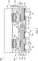
- FIG. 2 is a cross-sectional view of a semiconductor package assembly 500b in accordance with some embodiments of the disclosure. Elements of the embodiments hereinafter, that are the same or similar as those previously described with reference to FIG. 1 , are not repeated for brevity.
- the semiconductor package assembly 500b includes a base 250b.
- the base 250b includes a solder mask layer 216b covers the device-attach surface 201 of the core substrate 200a of the base 250b.
- the solder mask layer 216b may cover the conductive trace 206 directly on the through via plug 214.
- the solder mask layer 216b may prevent oxidation of the underlying conductive trace 206.
- the solder mask layer 216b has one or more openings 218b to expose the device pads 204. Also, the openings 218b of the solder mask layer 216b may be separated from the device pads 204 by a distance D.
- the openings 218b are separated from the device pads 204 to prevent conductive structures 322 of the semiconductor device 300 disposed on the device pads 204 from short-circuiting with other conductive lines and device pads. Also, the openings 218b of the solder mask layer 216b may provide positions for the conductive structures 322 of the semiconductor device 300 to be bonded thereon.
- the solder mask layer 216b and the solder mask layer 220 are formed of the same materials.
- the solder mask layer 216b and the core substrate 200a are formed of the same materials.
- the solder mask layer 216b may be formed of thermosetting materials, such as polypropylene (PP) resin.
- the solder mask layer 216b is formed of Ajinomoto build-up film (ABF).
- the solder mask layer 216b may include glass fibers 223 dispersed therein to reinforce the strength of the solder mask layer 220.
- FIG. 3 is a cross-sectional view of a semiconductor package assembly 500c in accordance with some embodiments of the disclosure. Elements of the embodiments hereinafter, that are the same or similar as those previously described with reference to FIG. 1 , are not repeated for brevity.
- the semiconductor package assembly 500c includes a base 250c.
- the semiconductor package assembly 500c is fabricated without the solder mask layer 200 shown in FIGS. 1 and 2 .
- the base 250c of the semiconductor package assembly 500c may require a single solder mask layer (e.g. a solder mask layer 216a) disposed between a semiconductor device (e.g. the semiconductor device 300) and the base 250c.
- the base 250c includes a core substrate 200b, device pads 204, a conductive plug structure 235 and the solder mask layer 216a.
- the base 250c includes a printed circuit board (PCB).
- FIG. 3 is also used to illustrate one exemplary embodiment of a method for fabricating the base 250c.
- the core substrate 200b of the base 250c is provided.
- the core substrate 200b may include a device-attach surface 201 and a solder-bump-attach surface 203 opposite to the device-attach surface 201.
- the device-attach surface 201 of the core substrate 200b is provided for the semiconductor device 300 disposed thereon.
- the solder-bump-attach surface 203 of the core substrate 200b is provided for the solder-bump structures 226 disposed thereon.
- the core substrate 200b is formed of thermosetting materials.
- the core substrate 200b is formed of resin-base materials.
- the core substrate 200b may be formed of paper phenolic resin, composite epoxy, polyimide resin BT (Bismaleimide-Triazine) resin or polypropylene (PP) resin.
- the core substrate 200b comprises glass fibers 205 dispersed therein to reinforce the strength of the base 250c. In some embodiments, the glass fibers 205 are optional.
- trenches 236 are formed in a portion of the core substrate 200b and close to the device-attach surface 201 of the core substrate 200b.
- the trenches 236 may be extended downwardly from the device-attach surface 201 of the core substrate 200b.
- the trenches 236 are formed by the laser drilling process or chemical etching process, and the subsequent cleaning process (e.g. a desmear process).
- the conductive plug structures 235 of the base 250c are respectively formed filling the trenches 236 after the formation of the trenches 236.
- the conductive plug structures 235 may be formed passing through a portion of the core substrate 200b.
- the device pads 204 are formed on the device-attach surface 201 of the core substrate 200b.
- the device pads 204 are formed simultaneously with the conductive plug structures 235.
- each of the conductive plug structures 235 has a top portion 232 and a bottom portion 234 connecting to the top portion 232. The top portion 232 of the each of the conductive plug structures 235 may be formed on the device-attach surface 201 of the core substrate 200b.
- the bottom portion 234 of the each of the conductive plug structures 235 may be embedded in the base 250c and surrounded by the core substrate 200b.
- the conductive plug structures 235 and the device pads 204 are formed by the electro-plating process and the subsequent patterning process.
- the solder mask layer 216a is formed covering the device-attach surface 201 of the core substrate 200b.
- the solder mask layer 216a may cover the conductive plug structures 235.
- the solder mask layer 216a may prevent oxidation of the underlying conductive plug structures 235.
- the solder mask layer 216a has one or more openings 218a to expose the device pads 204.
- the openings 218a of the solder mask layer 216a may be separated from the device pads 204 by a distance D.
- the openings 218a are separated from the device pads 204 to prevent conductive structures 322 of the semiconductor device 300 disposed on the device pads 204 from short-circuiting with other conductive lines and device pads.
- the openings 218a of the solder mask layer 216a may provide positions for the conductive structures 322 of the semiconductor device 300 to be bonded thereon.
- the solder mask layer 216a includes solder-resistant materials.
- the solder mask layer 216a may include photocuring materials, such as photoimageable solder mask materials.
- the solder mask layer 216a may include solder mask, or insulating materials including polyimide, Ajinomoto build-up film (ABF), epoxy, polymethylmethacrylate (PMMA) resin, a composite including epoxy and PMMA resin, or polypropylene (PP) resin.
- the solder mask layer 216a and the core substrate 200b are formed of different materials.
- the solder mask layer 216a may be formed by a coating, a printing process, an adhesion process, a laminating process or another appropriate process.
- solder mask layer 216a of the semiconductor package assembly 500c is replaced by the solder mask layer 216b shown in FIG. 2 .
- the solder mask layer 216b and the core substrate 200b are formed of the same materials.
- trenches 240 are formed in a portion of the core substrate 200b and close to the solder-bump-attach surface 203 of the core substrate 200b after the formation of the solder mask layer 216a.
- the trenches 240 may be aligned to the corresponding trenches 236.
- the trenches 240 may be extended upwardly from the solder-bump-attach surface 203 of the core substrate 200b.
- the bottom portion 234 of the each of the conductive plug structures 235 is exposed to a bottom of the corresponding trench 240.
- the trenches 240 are formed by the laser drilling process or chemical etching process, and the subsequent cleaning process (e.g. a desmear process).
- the base 250c is formed, as shown in FIG. 3 in accordance with some embodiments.
- Ni/Au layer structures 207 are formed on the device pads 204 and the bottom portion 234 of the each of the conductive plug structures 235 by the electro-plating process. In some embodiments, the Ni/Au layer structures 207 are optional.
- the semiconductor device 300 is mounted on the device-attach surface 201 of the core substrate 200b of the base 250c with an active surface of the semiconductor device 300 facing the base 250c by a bonding process.
- the solder-bump structures 226 are formed on the bottom portion 234 of the corresponding conductive plug structures 235.
- the solder-bump structures 226 may be formed filling the trenches 240 of the core substrate 200b and electrically connected to the bottom portions 234 of the corresponding conductive plug structures 235. Therefore, the bottom portion 234 of the conductive plug structures 235 may serve as bump pad of the base 250c.
- a surface 242 of the bump pad i.e.
- the bottom portion 234 of the conductive plug structure 235 is between the device-attach surface 201 and the solder-bump structures 226 of the core substrate 200b. Because the bump pad of the base 250a is the bottom portion 234 of the conductive plug structure 235, a boundary 233 of the bump pad (i.e. the bottom portion 234 of the conductive plug structure 235) is (or is aligned to) a boundary of the conductive plug structure 235.
- the solder-bump structures 226 may be formed on the bottom portions 234 of the corresponding conductive plug structures 235 by a deposition process and a patterning process, or printing process/ ball attachment process.
- the bottom portion 234 of the conductive plug structure 235 serves as a bump pad of the base 250c.
- the solder-bump structure 226 e.g. a solder-ball
- the base 250c of the semiconductor package assembly 500c is fabricated without forming an additional solder mask layer on the solder-bump surface 302 of the core substrate 200b. Therefore, the semiconductor package assembly 500c may require a single solder mask layer (e.g.
- solder mask layer 216a or 216b disposed on the device-attach surface 201 of the core substrate 200b.
- the problem of cracks forming at the interface between the solder-bump structure and the solder mask layer on the solder-bump-attach surface of the core substrate of the base can be avoided.
- Embodiments provide a semiconductor package assembly.
- the semiconductor package assembly includes a base including a core substrate having a device-attach surface and a solder-bump-attach surface opposite to the device-attach surface.
- the base of the semiconductor package assembly includes a first solder mask layer disposed on the solder-bump-attach surface and a second solder mask layer disposed on the device-attach surface.
- the first solder mask layer and the core substrate are formed of a first material
- the second older mask layer is formed of a second material.
- the first solder mask layer covers the solder-bump-attach surface of the core substrate may be formed of the materials that is similar to or the same as the material of the core substrate (e.g. a thermosetting material).
- the first solder mask layer may help to balance the stress applied on the core substrate due to the mismatch of CTE between the core substrate and the second solder mask layer, which is disposed on the device-attach surface of the core substrate. Therefore, the reliability of the semiconductor package assembly is improved. In addition, the problem of cracks forming at the interface between the solder mask layer and the solder-bump structure on the solder-bump-attach surface of the core substrate of the base can be avoided.
- the core substrate, the first solder mask layer on the solder-bump-attach surface of the core substrate and the second solder mask layer on the device-attach surface of the core substrate are formed of the same material, for example, a thermosetting material.
- the first solder mask layer and the second solder mask layer of the base may further reduce the mismatch of CTE between the core substrate and the solder mask layers respectively disposed on the device-attach surface and the solder-bump-attach surface of the core substrate. Therefore, the thermal cycling reliability of the semiconductor package assembly is improved.
- the base of the semiconductor package assembly includes a conductive plug structure formed extended in to a portion of the core substrate from the device-attach surface of the core substrate.
- the conductive plug structure may have a top portion and a bottom portion connecting to the top portion.
- the top portion of the conductive plug structure is formed on the device-attach surface of the core substrate and serves as a conductive trace.
- the bottom portion of the conductive plug structure is formed embedded in the of the core substrate without protruding from the core substrate.
- the bottom portion of the conductive plug structure which is close to the bump-attach surface of the core substrate, serves as a bump pad of the base.
- the solder-bump structure e.g.
- a solder-ball may be formed extended a portion of the core substrate form the solder-bump-attach surface to electrically connect to a corresponding bump pad. Therefore, the semiconductor package assembly may require a single solder mask layer disposed on the device-attach surface of the core substrate. The problem of cracks forming at the interface between the solder-bump structure and the solder mask layer on the solder-bump-attach surface of the core substrate of the base can be avoided.
Landscapes
- Wire Bonding (AREA)
- Production Of Multi-Layered Print Wiring Board (AREA)
Applications Claiming Priority (3)
| Application Number | Priority Date | Filing Date | Title |
|---|---|---|---|
| US201662401280P | 2016-09-29 | 2016-09-29 | |
| US15/638,472 US10276465B2 (en) | 2016-09-29 | 2017-06-30 | Semiconductor package assembly |
| EP17189307.6A EP3301712B1 (de) | 2016-09-29 | 2017-09-05 | Halbleitergehäuseanordnung |
Related Parent Applications (2)
| Application Number | Title | Priority Date | Filing Date |
|---|---|---|---|
| EP17189307.6A Division EP3301712B1 (de) | 2016-09-29 | 2017-09-05 | Halbleitergehäuseanordnung |
| EP17189307.6A Division-Into EP3301712B1 (de) | 2016-09-29 | 2017-09-05 | Halbleitergehäuseanordnung |
Publications (2)
| Publication Number | Publication Date |
|---|---|
| EP3971963A1 true EP3971963A1 (de) | 2022-03-23 |
| EP3971963B1 EP3971963B1 (de) | 2024-12-11 |
Family
ID=59790979
Family Applications (2)
| Application Number | Title | Priority Date | Filing Date |
|---|---|---|---|
| EP21200916.1A Active EP3971963B1 (de) | 2016-09-29 | 2017-09-05 | Halbleitergehäuseanordnung |
| EP17189307.6A Active EP3301712B1 (de) | 2016-09-29 | 2017-09-05 | Halbleitergehäuseanordnung |
Family Applications After (1)
| Application Number | Title | Priority Date | Filing Date |
|---|---|---|---|
| EP17189307.6A Active EP3301712B1 (de) | 2016-09-29 | 2017-09-05 | Halbleitergehäuseanordnung |
Country Status (4)
| Country | Link |
|---|---|
| US (1) | US10276465B2 (de) |
| EP (2) | EP3971963B1 (de) |
| CN (1) | CN107887348A (de) |
| TW (1) | TWI656610B (de) |
Families Citing this family (5)
| Publication number | Priority date | Publication date | Assignee | Title |
|---|---|---|---|---|
| KR102538178B1 (ko) * | 2018-08-22 | 2023-05-31 | 삼성전자주식회사 | 유기 인터포저를 포함하는 반도체 패키지 |
| US10748857B2 (en) * | 2018-09-11 | 2020-08-18 | Micron Technology, Inc. | Die features for self-alignment during die bonding |
| FI130884B1 (fi) * | 2021-07-06 | 2024-05-08 | Teknologian Tutkimuskeskus Vtt Oy | Liitosrakenne |
| CN116453962A (zh) * | 2022-01-07 | 2023-07-18 | 长鑫存储技术有限公司 | 半导体结构及其形成方法 |
| US12191271B2 (en) | 2022-01-07 | 2025-01-07 | Changxin Memory Technologies, Inc. | Semiconductor structure comprising up-narrow and down-wide openings and forming method thereof |
Citations (7)
| Publication number | Priority date | Publication date | Assignee | Title |
|---|---|---|---|---|
| US20040137659A1 (en) * | 2002-08-15 | 2004-07-15 | Yi-Chuan Ding | [method of fabricating a solder mask and structure of a substrate] |
| US20110084370A1 (en) | 2009-10-14 | 2011-04-14 | Advanced Semiconductor Engineering, Inc. | Semiconductor package and process for fabricating same |
| US20110169150A1 (en) | 2010-01-13 | 2011-07-14 | Advanced Semiconductor Engineering, Inc. | Semiconductor Package with Single Sided Substrate Design and Manufacturing Methods Thereof |
| US20130251967A1 (en) | 2012-03-22 | 2013-09-26 | Nvidia Corporation | System, method, and computer program product for controlling warping of a substrate |
| US9171739B1 (en) | 2014-06-24 | 2015-10-27 | Stats Chippac Ltd. | Integrated circuit packaging system with coreless substrate and method of manufacture thereof |
| US20160126175A1 (en) * | 2014-11-04 | 2016-05-05 | Via Alliance Semiconductor Co., Ltd. | Circuit substrate and semiconductor package structure |
| EP3051583A1 (de) | 2013-09-27 | 2016-08-03 | Renesas Electronics Corporation | Halbleiterbauelement und herstellungsverfahren dafür |
Family Cites Families (9)
| Publication number | Priority date | Publication date | Assignee | Title |
|---|---|---|---|---|
| TW471148B (en) | 2000-11-21 | 2002-01-01 | Phoenix Prec Technology Corp | Integrated circuit packaging substrate structure and the manufacturing method thereof |
| US6506633B1 (en) * | 2002-02-15 | 2003-01-14 | Unimicron Technology Corp. | Method of fabricating a multi-chip module package |
| TWI304255B (en) | 2006-08-31 | 2008-12-11 | Phoenix Prec Technology Corp | A capacitance element embedded in semiconductor package substrate structure and method for fabricating tme same |
| KR100867148B1 (ko) | 2007-09-28 | 2008-11-06 | 삼성전기주식회사 | 인쇄회로기판 및 그 제조방법 |
| US7919851B2 (en) * | 2008-06-05 | 2011-04-05 | Powertech Technology Inc. | Laminate substrate and semiconductor package utilizing the substrate |
| TWI370711B (en) | 2009-01-06 | 2012-08-11 | Nan Ya Printed Circuit Board | Fine line structure with improved adhesion and method for fabricating the same |
| TWI538137B (zh) * | 2010-03-04 | 2016-06-11 | 日月光半導體製造股份有限公司 | 具有單側基板設計的半導體封裝及其製造方法 |
| KR20150002492A (ko) | 2013-06-28 | 2015-01-07 | 쿄세라 서킷 솔루션즈 가부시키가이샤 | 배선 기판 |
| US9521752B2 (en) | 2014-09-19 | 2016-12-13 | Harris Corporation | Method of making an electronic device having a thin film resistor formed on an LCP solder mask and related devices |
-
2017
- 2017-06-30 US US15/638,472 patent/US10276465B2/en active Active
- 2017-08-30 TW TW106129514A patent/TWI656610B/zh not_active IP Right Cessation
- 2017-08-30 CN CN201710762051.1A patent/CN107887348A/zh not_active Withdrawn
- 2017-09-05 EP EP21200916.1A patent/EP3971963B1/de active Active
- 2017-09-05 EP EP17189307.6A patent/EP3301712B1/de active Active
Patent Citations (7)
| Publication number | Priority date | Publication date | Assignee | Title |
|---|---|---|---|---|
| US20040137659A1 (en) * | 2002-08-15 | 2004-07-15 | Yi-Chuan Ding | [method of fabricating a solder mask and structure of a substrate] |
| US20110084370A1 (en) | 2009-10-14 | 2011-04-14 | Advanced Semiconductor Engineering, Inc. | Semiconductor package and process for fabricating same |
| US20110169150A1 (en) | 2010-01-13 | 2011-07-14 | Advanced Semiconductor Engineering, Inc. | Semiconductor Package with Single Sided Substrate Design and Manufacturing Methods Thereof |
| US20130251967A1 (en) | 2012-03-22 | 2013-09-26 | Nvidia Corporation | System, method, and computer program product for controlling warping of a substrate |
| EP3051583A1 (de) | 2013-09-27 | 2016-08-03 | Renesas Electronics Corporation | Halbleiterbauelement und herstellungsverfahren dafür |
| US9171739B1 (en) | 2014-06-24 | 2015-10-27 | Stats Chippac Ltd. | Integrated circuit packaging system with coreless substrate and method of manufacture thereof |
| US20160126175A1 (en) * | 2014-11-04 | 2016-05-05 | Via Alliance Semiconductor Co., Ltd. | Circuit substrate and semiconductor package structure |
Also Published As
| Publication number | Publication date |
|---|---|
| EP3971963B1 (de) | 2024-12-11 |
| US10276465B2 (en) | 2019-04-30 |
| EP3301712B1 (de) | 2021-11-10 |
| EP3301712A1 (de) | 2018-04-04 |
| TW201830591A (zh) | 2018-08-16 |
| CN107887348A (zh) | 2018-04-06 |
| TWI656610B (zh) | 2019-04-11 |
| US20180090408A1 (en) | 2018-03-29 |
Similar Documents
| Publication | Publication Date | Title |
|---|---|---|
| US9165878B2 (en) | Semiconductor packages and methods of packaging semiconductor devices | |
| JP5183949B2 (ja) | 半導体装置の製造方法 | |
| US7902660B1 (en) | Substrate for semiconductor device and manufacturing method thereof | |
| US10580747B2 (en) | Semiconductor package and method for fabricating base for semiconductor package | |
| EP4235762B1 (de) | Halbleiterpaket und verfahren zur herstellung einer basis für das halbleiterpaket | |
| TWI541916B (zh) | 形成覆晶互連結構的半導體裝置和方法 | |
| US6969674B2 (en) | Structure and method for fine pitch flip chip substrate | |
| EP3971963B1 (de) | Halbleitergehäuseanordnung | |
| TWI495026B (zh) | 晶片封裝基板和結構及其製作方法 | |
| KR102826729B1 (ko) | 반도체 장치 및 이의 제조 방법 | |
| CN106816388A (zh) | 半导体封装结构及其制作方法 | |
| EP3024026B1 (de) | Halbleitergehäuse | |
| JP3654116B2 (ja) | 半導体装置及びその製造方法、回路基板並びに電子機器 | |
| KR101009187B1 (ko) | 인쇄회로기판 및 그 제조방법 | |
| JP4051570B2 (ja) | 半導体装置の製造方法 | |
| CN101510515B (zh) | 线路板及其制作方法及芯片封装结构 | |
| CN118251971A (zh) | 电路板和包括该电路板的半导体封装 | |
| JP4525148B2 (ja) | 半導体装置およびその製造方法 | |
| KR20080045017A (ko) | 금속 범프를 갖는 반도체 칩 패키지 및 그 제조방법 | |
| KR20110013902A (ko) | 패키지 및 그 제조방법 | |
| JP4561969B2 (ja) | 半導体装置 | |
| JP4696712B2 (ja) | 半導体装置 | |
| JP2007266640A (ja) | 半導体装置及びその製造方法、回路基板並びに電子機器 | |
| JP2006032632A (ja) | 実装構造およびその製造方法 | |
| JP2007180593A (ja) | 半導体装置の製造方法 |
Legal Events
| Date | Code | Title | Description |
|---|---|---|---|
| PUAI | Public reference made under article 153(3) epc to a published international application that has entered the european phase |
Free format text: ORIGINAL CODE: 0009012 |
|
| STAA | Information on the status of an ep patent application or granted ep patent |
Free format text: STATUS: THE APPLICATION HAS BEEN PUBLISHED |
|
| AC | Divisional application: reference to earlier application |
Ref document number: 3301712 Country of ref document: EP Kind code of ref document: P |
|
| AK | Designated contracting states |
Kind code of ref document: A1 Designated state(s): AL AT BE BG CH CY CZ DE DK EE ES FI FR GB GR HR HU IE IS IT LI LT LU LV MC MK MT NL NO PL PT RO RS SE SI SK SM TR |
|
| STAA | Information on the status of an ep patent application or granted ep patent |
Free format text: STATUS: REQUEST FOR EXAMINATION WAS MADE |
|
| 17P | Request for examination filed |
Effective date: 20220818 |
|
| RBV | Designated contracting states (corrected) |
Designated state(s): AL AT BE BG CH CY CZ DE DK EE ES FI FR GB GR HR HU IE IS IT LI LT LU LV MC MK MT NL NO PL PT RO RS SE SI SK SM TR |
|
| P01 | Opt-out of the competence of the unified patent court (upc) registered |
Effective date: 20230607 |
|
| GRAP | Despatch of communication of intention to grant a patent |
Free format text: ORIGINAL CODE: EPIDOSNIGR1 |
|
| STAA | Information on the status of an ep patent application or granted ep patent |
Free format text: STATUS: GRANT OF PATENT IS INTENDED |
|
| INTG | Intention to grant announced |
Effective date: 20240126 |
|
| RAP3 | Party data changed (applicant data changed or rights of an application transferred) |
Owner name: MEDIATEK INC. |
|
| RIN1 | Information on inventor provided before grant (corrected) |
Inventor name: TSAI, SHIANN-TSONG |
|
| GRAJ | Information related to disapproval of communication of intention to grant by the applicant or resumption of examination proceedings by the epo deleted |
Free format text: ORIGINAL CODE: EPIDOSDIGR1 |
|
| STAA | Information on the status of an ep patent application or granted ep patent |
Free format text: STATUS: REQUEST FOR EXAMINATION WAS MADE |
|
| INTC | Intention to grant announced (deleted) | ||
| GRAP | Despatch of communication of intention to grant a patent |
Free format text: ORIGINAL CODE: EPIDOSNIGR1 |
|
| STAA | Information on the status of an ep patent application or granted ep patent |
Free format text: STATUS: GRANT OF PATENT IS INTENDED |
|
| INTG | Intention to grant announced |
Effective date: 20240704 |
|
| GRAS | Grant fee paid |
Free format text: ORIGINAL CODE: EPIDOSNIGR3 |
|
| GRAA | (expected) grant |
Free format text: ORIGINAL CODE: 0009210 |
|
| STAA | Information on the status of an ep patent application or granted ep patent |
Free format text: STATUS: THE PATENT HAS BEEN GRANTED |
|
| AC | Divisional application: reference to earlier application |
Ref document number: 3301712 Country of ref document: EP Kind code of ref document: P |
|
| AK | Designated contracting states |
Kind code of ref document: B1 Designated state(s): AL AT BE BG CH CY CZ DE DK EE ES FI FR GB GR HR HU IE IS IT LI LT LU LV MC MK MT NL NO PL PT RO RS SE SI SK SM TR |
|
| REG | Reference to a national code |
Ref country code: GB Ref legal event code: FG4D |
|
| REG | Reference to a national code |
Ref country code: CH Ref legal event code: EP |
|
| REG | Reference to a national code |
Ref country code: IE Ref legal event code: FG4D |
|
| REG | Reference to a national code |
Ref country code: DE Ref legal event code: R096 Ref document number: 602017086783 Country of ref document: DE |
|
| REG | Reference to a national code |
Ref country code: LT Ref legal event code: MG9D |
|
| PG25 | Lapsed in a contracting state [announced via postgrant information from national office to epo] |
Ref country code: HR Free format text: LAPSE BECAUSE OF FAILURE TO SUBMIT A TRANSLATION OF THE DESCRIPTION OR TO PAY THE FEE WITHIN THE PRESCRIBED TIME-LIMIT Effective date: 20241211 |
|
| PG25 | Lapsed in a contracting state [announced via postgrant information from national office to epo] |
Ref country code: FI Free format text: LAPSE BECAUSE OF FAILURE TO SUBMIT A TRANSLATION OF THE DESCRIPTION OR TO PAY THE FEE WITHIN THE PRESCRIBED TIME-LIMIT Effective date: 20241211 |
|
| PG25 | Lapsed in a contracting state [announced via postgrant information from national office to epo] |
Ref country code: BG Free format text: LAPSE BECAUSE OF FAILURE TO SUBMIT A TRANSLATION OF THE DESCRIPTION OR TO PAY THE FEE WITHIN THE PRESCRIBED TIME-LIMIT Effective date: 20241211 |
|
| REG | Reference to a national code |
Ref country code: NL Ref legal event code: MP Effective date: 20241211 |
|
| PG25 | Lapsed in a contracting state [announced via postgrant information from national office to epo] |
Ref country code: ES Free format text: LAPSE BECAUSE OF FAILURE TO SUBMIT A TRANSLATION OF THE DESCRIPTION OR TO PAY THE FEE WITHIN THE PRESCRIBED TIME-LIMIT Effective date: 20241211 |
|
| PG25 | Lapsed in a contracting state [announced via postgrant information from national office to epo] |
Ref country code: NO Free format text: LAPSE BECAUSE OF FAILURE TO SUBMIT A TRANSLATION OF THE DESCRIPTION OR TO PAY THE FEE WITHIN THE PRESCRIBED TIME-LIMIT Effective date: 20250311 |
|
| PG25 | Lapsed in a contracting state [announced via postgrant information from national office to epo] |
Ref country code: LV Free format text: LAPSE BECAUSE OF FAILURE TO SUBMIT A TRANSLATION OF THE DESCRIPTION OR TO PAY THE FEE WITHIN THE PRESCRIBED TIME-LIMIT Effective date: 20241211 Ref country code: GR Free format text: LAPSE BECAUSE OF FAILURE TO SUBMIT A TRANSLATION OF THE DESCRIPTION OR TO PAY THE FEE WITHIN THE PRESCRIBED TIME-LIMIT Effective date: 20250312 |
|
| PG25 | Lapsed in a contracting state [announced via postgrant information from national office to epo] |
Ref country code: RS Free format text: LAPSE BECAUSE OF FAILURE TO SUBMIT A TRANSLATION OF THE DESCRIPTION OR TO PAY THE FEE WITHIN THE PRESCRIBED TIME-LIMIT Effective date: 20250311 |
|
| PG25 | Lapsed in a contracting state [announced via postgrant information from national office to epo] |
Ref country code: NL Free format text: LAPSE BECAUSE OF FAILURE TO SUBMIT A TRANSLATION OF THE DESCRIPTION OR TO PAY THE FEE WITHIN THE PRESCRIBED TIME-LIMIT Effective date: 20241211 |
|
| REG | Reference to a national code |
Ref country code: AT Ref legal event code: MK05 Ref document number: 1751087 Country of ref document: AT Kind code of ref document: T Effective date: 20241211 |
|
| PG25 | Lapsed in a contracting state [announced via postgrant information from national office to epo] |
Ref country code: SM Free format text: LAPSE BECAUSE OF FAILURE TO SUBMIT A TRANSLATION OF THE DESCRIPTION OR TO PAY THE FEE WITHIN THE PRESCRIBED TIME-LIMIT Effective date: 20241211 |
|
| PG25 | Lapsed in a contracting state [announced via postgrant information from national office to epo] |
Ref country code: PL Free format text: LAPSE BECAUSE OF FAILURE TO SUBMIT A TRANSLATION OF THE DESCRIPTION OR TO PAY THE FEE WITHIN THE PRESCRIBED TIME-LIMIT Effective date: 20241211 |
|
| PG25 | Lapsed in a contracting state [announced via postgrant information from national office to epo] |
Ref country code: IS Free format text: LAPSE BECAUSE OF FAILURE TO SUBMIT A TRANSLATION OF THE DESCRIPTION OR TO PAY THE FEE WITHIN THE PRESCRIBED TIME-LIMIT Effective date: 20250411 |
|
| PG25 | Lapsed in a contracting state [announced via postgrant information from national office to epo] |
Ref country code: PT Free format text: LAPSE BECAUSE OF FAILURE TO SUBMIT A TRANSLATION OF THE DESCRIPTION OR TO PAY THE FEE WITHIN THE PRESCRIBED TIME-LIMIT Effective date: 20250411 |
|
| PG25 | Lapsed in a contracting state [announced via postgrant information from national office to epo] |
Ref country code: EE Free format text: LAPSE BECAUSE OF FAILURE TO SUBMIT A TRANSLATION OF THE DESCRIPTION OR TO PAY THE FEE WITHIN THE PRESCRIBED TIME-LIMIT Effective date: 20241211 |
|
| PG25 | Lapsed in a contracting state [announced via postgrant information from national office to epo] |
Ref country code: RO Free format text: LAPSE BECAUSE OF FAILURE TO SUBMIT A TRANSLATION OF THE DESCRIPTION OR TO PAY THE FEE WITHIN THE PRESCRIBED TIME-LIMIT Effective date: 20241211 Ref country code: AT Free format text: LAPSE BECAUSE OF FAILURE TO SUBMIT A TRANSLATION OF THE DESCRIPTION OR TO PAY THE FEE WITHIN THE PRESCRIBED TIME-LIMIT Effective date: 20241211 |
|
| PG25 | Lapsed in a contracting state [announced via postgrant information from national office to epo] |
Ref country code: SK Free format text: LAPSE BECAUSE OF FAILURE TO SUBMIT A TRANSLATION OF THE DESCRIPTION OR TO PAY THE FEE WITHIN THE PRESCRIBED TIME-LIMIT Effective date: 20241211 |
|
| PG25 | Lapsed in a contracting state [announced via postgrant information from national office to epo] |
Ref country code: CZ Free format text: LAPSE BECAUSE OF FAILURE TO SUBMIT A TRANSLATION OF THE DESCRIPTION OR TO PAY THE FEE WITHIN THE PRESCRIBED TIME-LIMIT Effective date: 20241211 |
|
| PG25 | Lapsed in a contracting state [announced via postgrant information from national office to epo] |
Ref country code: IT Free format text: LAPSE BECAUSE OF FAILURE TO SUBMIT A TRANSLATION OF THE DESCRIPTION OR TO PAY THE FEE WITHIN THE PRESCRIBED TIME-LIMIT Effective date: 20241211 |
|
| PG25 | Lapsed in a contracting state [announced via postgrant information from national office to epo] |
Ref country code: SE Free format text: LAPSE BECAUSE OF FAILURE TO SUBMIT A TRANSLATION OF THE DESCRIPTION OR TO PAY THE FEE WITHIN THE PRESCRIBED TIME-LIMIT Effective date: 20241211 |
|
| REG | Reference to a national code |
Ref country code: DE Ref legal event code: R097 Ref document number: 602017086783 Country of ref document: DE |
|
| PG25 | Lapsed in a contracting state [announced via postgrant information from national office to epo] |
Ref country code: DK Free format text: LAPSE BECAUSE OF FAILURE TO SUBMIT A TRANSLATION OF THE DESCRIPTION OR TO PAY THE FEE WITHIN THE PRESCRIBED TIME-LIMIT Effective date: 20241211 |
|
| PGFP | Annual fee paid to national office [announced via postgrant information from national office to epo] |
Ref country code: DE Payment date: 20250702 Year of fee payment: 9 |
|
| PGFP | Annual fee paid to national office [announced via postgrant information from national office to epo] |
Ref country code: GB Payment date: 20250703 Year of fee payment: 9 |
|
| PLBE | No opposition filed within time limit |
Free format text: ORIGINAL CODE: 0009261 |
|
| STAA | Information on the status of an ep patent application or granted ep patent |
Free format text: STATUS: NO OPPOSITION FILED WITHIN TIME LIMIT |
|
| PGFP | Annual fee paid to national office [announced via postgrant information from national office to epo] |
Ref country code: FR Payment date: 20250703 Year of fee payment: 9 |
|
| REG | Reference to a national code |
Ref country code: CH Ref legal event code: L10 Free format text: ST27 STATUS EVENT CODE: U-0-0-L10-L00 (AS PROVIDED BY THE NATIONAL OFFICE) Effective date: 20251022 |
|
| 26N | No opposition filed |
Effective date: 20250912 |
|
| REG | Reference to a national code |
Ref country code: DE Ref legal event code: R079 Ref document number: 602017086783 Country of ref document: DE Free format text: PREVIOUS MAIN CLASS: H01L0023498000 Ipc: H10W0070620000 |
|
| REG | Reference to a national code |
Ref country code: CH Ref legal event code: H13 Free format text: ST27 STATUS EVENT CODE: U-0-0-H10-H13 (AS PROVIDED BY THE NATIONAL OFFICE) Effective date: 20260504 |