EP3964084B1 - Power supply unit for aerosol generation device - Google Patents
Power supply unit for aerosol generation device Download PDFInfo
- Publication number
- EP3964084B1 EP3964084B1 EP21194267.7A EP21194267A EP3964084B1 EP 3964084 B1 EP3964084 B1 EP 3964084B1 EP 21194267 A EP21194267 A EP 21194267A EP 3964084 B1 EP3964084 B1 EP 3964084B1
- Authority
- EP
- European Patent Office
- Prior art keywords
- power supply
- connector
- terminal
- communication
- external device
- Prior art date
- Legal status (The legal status is an assumption and is not a legal conclusion. Google has not performed a legal analysis and makes no representation as to the accuracy of the status listed.)
- Active
Links
- 239000000443 aerosol Substances 0.000 title claims description 54
- 238000004891 communication Methods 0.000 claims description 212
- 230000004044 response Effects 0.000 claims description 3
- 239000002775 capsule Substances 0.000 description 14
- 239000000796 flavoring agent Substances 0.000 description 14
- 235000019634 flavors Nutrition 0.000 description 14
- 238000000034 method Methods 0.000 description 13
- 230000003071 parasitic effect Effects 0.000 description 13
- 235000019504 cigarettes Nutrition 0.000 description 8
- 239000000463 material Substances 0.000 description 8
- 238000010438 heat treatment Methods 0.000 description 7
- 238000001514 detection method Methods 0.000 description 5
- 238000007599 discharging Methods 0.000 description 5
- 230000002441 reversible effect Effects 0.000 description 5
- 238000010586 diagram Methods 0.000 description 4
- 239000007788 liquid Substances 0.000 description 4
- DNIAPMSPPWPWGF-UHFFFAOYSA-N Propylene glycol Chemical compound CC(O)CO DNIAPMSPPWPWGF-UHFFFAOYSA-N 0.000 description 3
- 230000005611 electricity Effects 0.000 description 3
- 230000036541 health Effects 0.000 description 3
- 210000000214 mouth Anatomy 0.000 description 3
- 238000012545 processing Methods 0.000 description 3
- 230000003068 static effect Effects 0.000 description 3
- PEDCQBHIVMGVHV-UHFFFAOYSA-N Glycerine Chemical compound OCC(O)CO PEDCQBHIVMGVHV-UHFFFAOYSA-N 0.000 description 2
- 239000003990 capacitor Substances 0.000 description 2
- 239000003814 drug Substances 0.000 description 2
- 230000002265 prevention Effects 0.000 description 2
- 239000007787 solid Substances 0.000 description 2
- NOOLISFMXDJSKH-UTLUCORTSA-N (+)-Neomenthol Chemical compound CC(C)[C@@H]1CC[C@@H](C)C[C@@H]1O NOOLISFMXDJSKH-UTLUCORTSA-N 0.000 description 1
- NOOLISFMXDJSKH-UHFFFAOYSA-N DL-menthol Natural products CC(C)C1CCC(C)CC1O NOOLISFMXDJSKH-UHFFFAOYSA-N 0.000 description 1
- 241000196324 Embryophyta Species 0.000 description 1
- LFQSCWFLJHTTHZ-UHFFFAOYSA-N Ethanol Chemical compound CCO LFQSCWFLJHTTHZ-UHFFFAOYSA-N 0.000 description 1
- HBBGRARXTFLTSG-UHFFFAOYSA-N Lithium ion Chemical compound [Li+] HBBGRARXTFLTSG-UHFFFAOYSA-N 0.000 description 1
- 235000006679 Mentha X verticillata Nutrition 0.000 description 1
- 235000002899 Mentha suaveolens Nutrition 0.000 description 1
- 235000001636 Mentha x rotundifolia Nutrition 0.000 description 1
- 241000533293 Sesbania emerus Species 0.000 description 1
- 230000005856 abnormality Effects 0.000 description 1
- 230000003213 activating effect Effects 0.000 description 1
- 238000012387 aerosolization Methods 0.000 description 1
- 238000009529 body temperature measurement Methods 0.000 description 1
- 239000000919 ceramic Substances 0.000 description 1
- 230000008859 change Effects 0.000 description 1
- 230000003247 decreasing effect Effects 0.000 description 1
- 230000001419 dependent effect Effects 0.000 description 1
- 229940079593 drug Drugs 0.000 description 1
- 239000003571 electronic cigarette Substances 0.000 description 1
- 239000000835 fiber Substances 0.000 description 1
- 230000005669 field effect Effects 0.000 description 1
- 239000003205 fragrance Substances 0.000 description 1
- 239000003365 glass fiber Substances 0.000 description 1
- 235000011187 glycerol Nutrition 0.000 description 1
- 238000003780 insertion Methods 0.000 description 1
- 230000037431 insertion Effects 0.000 description 1
- 239000008263 liquid aerosol Substances 0.000 description 1
- 229910001416 lithium ion Inorganic materials 0.000 description 1
- 210000004072 lung Anatomy 0.000 description 1
- 229940041616 menthol Drugs 0.000 description 1
- 229910052751 metal Inorganic materials 0.000 description 1
- 239000002184 metal Substances 0.000 description 1
- 239000000203 mixture Substances 0.000 description 1
- 238000000465 moulding Methods 0.000 description 1
- 230000002093 peripheral effect Effects 0.000 description 1
- 239000011148 porous material Substances 0.000 description 1
- 230000008569 process Effects 0.000 description 1
- 230000001737 promoting effect Effects 0.000 description 1
- 230000003252 repetitive effect Effects 0.000 description 1
- 230000004043 responsiveness Effects 0.000 description 1
- 239000007921 spray Substances 0.000 description 1
- 238000005507 spraying Methods 0.000 description 1
- XLYOFNOQVPJJNP-UHFFFAOYSA-N water Substances O XLYOFNOQVPJJNP-UHFFFAOYSA-N 0.000 description 1
Images


Classifications
-
- A—HUMAN NECESSITIES
- A24—TOBACCO; CIGARS; CIGARETTES; SIMULATED SMOKING DEVICES; SMOKERS' REQUISITES
- A24F—SMOKERS' REQUISITES; MATCH BOXES; SIMULATED SMOKING DEVICES
- A24F40/00—Electrically operated smoking devices; Component parts thereof; Manufacture thereof; Maintenance or testing thereof; Charging means specially adapted therefor
- A24F40/50—Control or monitoring
-
- H—ELECTRICITY
- H02—GENERATION; CONVERSION OR DISTRIBUTION OF ELECTRIC POWER
- H02J—CIRCUIT ARRANGEMENTS OR SYSTEMS FOR SUPPLYING OR DISTRIBUTING ELECTRIC POWER; SYSTEMS FOR STORING ELECTRIC ENERGY
- H02J7/00—Circuit arrangements for charging or depolarising batteries or for supplying loads from batteries
- H02J7/0029—Circuit arrangements for charging or depolarising batteries or for supplying loads from batteries with safety or protection devices or circuits
- H02J7/0036—Circuit arrangements for charging or depolarising batteries or for supplying loads from batteries with safety or protection devices or circuits using connection detecting circuits
-
- A—HUMAN NECESSITIES
- A24—TOBACCO; CIGARS; CIGARETTES; SIMULATED SMOKING DEVICES; SMOKERS' REQUISITES
- A24F—SMOKERS' REQUISITES; MATCH BOXES; SIMULATED SMOKING DEVICES
- A24F40/00—Electrically operated smoking devices; Component parts thereof; Manufacture thereof; Maintenance or testing thereof; Charging means specially adapted therefor
- A24F40/65—Devices with integrated communication means, e.g. Wi-Fi
-
- A—HUMAN NECESSITIES
- A24—TOBACCO; CIGARS; CIGARETTES; SIMULATED SMOKING DEVICES; SMOKERS' REQUISITES
- A24F—SMOKERS' REQUISITES; MATCH BOXES; SIMULATED SMOKING DEVICES
- A24F40/00—Electrically operated smoking devices; Component parts thereof; Manufacture thereof; Maintenance or testing thereof; Charging means specially adapted therefor
- A24F40/40—Constructional details, e.g. connection of cartridges and battery parts
- A24F40/46—Shape or structure of electric heating means
-
- A—HUMAN NECESSITIES
- A24—TOBACCO; CIGARS; CIGARETTES; SIMULATED SMOKING DEVICES; SMOKERS' REQUISITES
- A24F—SMOKERS' REQUISITES; MATCH BOXES; SIMULATED SMOKING DEVICES
- A24F40/00—Electrically operated smoking devices; Component parts thereof; Manufacture thereof; Maintenance or testing thereof; Charging means specially adapted therefor
- A24F40/90—Arrangements or methods specially adapted for charging batteries thereof
- A24F40/95—Arrangements or methods specially adapted for charging batteries thereof structurally associated with cases
-
- H—ELECTRICITY
- H02—GENERATION; CONVERSION OR DISTRIBUTION OF ELECTRIC POWER
- H02J—CIRCUIT ARRANGEMENTS OR SYSTEMS FOR SUPPLYING OR DISTRIBUTING ELECTRIC POWER; SYSTEMS FOR STORING ELECTRIC ENERGY
- H02J7/00—Circuit arrangements for charging or depolarising batteries or for supplying loads from batteries
- H02J7/00032—Circuit arrangements for charging or depolarising batteries or for supplying loads from batteries characterised by data exchange
- H02J7/00034—Charger exchanging data with an electronic device, i.e. telephone, whose internal battery is under charge
-
- H—ELECTRICITY
- H02—GENERATION; CONVERSION OR DISTRIBUTION OF ELECTRIC POWER
- H02J—CIRCUIT ARRANGEMENTS OR SYSTEMS FOR SUPPLYING OR DISTRIBUTING ELECTRIC POWER; SYSTEMS FOR STORING ELECTRIC ENERGY
- H02J7/00—Circuit arrangements for charging or depolarising batteries or for supplying loads from batteries
- H02J7/00032—Circuit arrangements for charging or depolarising batteries or for supplying loads from batteries characterised by data exchange
- H02J7/00036—Charger exchanging data with battery
-
- H—ELECTRICITY
- H02—GENERATION; CONVERSION OR DISTRIBUTION OF ELECTRIC POWER
- H02J—CIRCUIT ARRANGEMENTS OR SYSTEMS FOR SUPPLYING OR DISTRIBUTING ELECTRIC POWER; SYSTEMS FOR STORING ELECTRIC ENERGY
- H02J7/00—Circuit arrangements for charging or depolarising batteries or for supplying loads from batteries
- H02J7/0063—Circuit arrangements for charging or depolarising batteries or for supplying loads from batteries with circuits adapted for supplying loads from the battery
-
- H—ELECTRICITY
- H02—GENERATION; CONVERSION OR DISTRIBUTION OF ELECTRIC POWER
- H02M—APPARATUS FOR CONVERSION BETWEEN AC AND AC, BETWEEN AC AND DC, OR BETWEEN DC AND DC, AND FOR USE WITH MAINS OR SIMILAR POWER SUPPLY SYSTEMS; CONVERSION OF DC OR AC INPUT POWER INTO SURGE OUTPUT POWER; CONTROL OR REGULATION THEREOF
- H02M1/00—Details of apparatus for conversion
- H02M1/0003—Details of control, feedback or regulation circuits
-
- H—ELECTRICITY
- H05—ELECTRIC TECHNIQUES NOT OTHERWISE PROVIDED FOR
- H05B—ELECTRIC HEATING; ELECTRIC LIGHT SOURCES NOT OTHERWISE PROVIDED FOR; CIRCUIT ARRANGEMENTS FOR ELECTRIC LIGHT SOURCES, IN GENERAL
- H05B1/00—Details of electric heating devices
- H05B1/02—Automatic switching arrangements specially adapted to apparatus ; Control of heating devices
- H05B1/0227—Applications
- H05B1/0297—Heating of fluids for non specified applications
-
- H—ELECTRICITY
- H05—ELECTRIC TECHNIQUES NOT OTHERWISE PROVIDED FOR
- H05B—ELECTRIC HEATING; ELECTRIC LIGHT SOURCES NOT OTHERWISE PROVIDED FOR; CIRCUIT ARRANGEMENTS FOR ELECTRIC LIGHT SOURCES, IN GENERAL
- H05B3/00—Ohmic-resistance heating
- H05B3/0014—Devices wherein the heating current flows through particular resistances
-
- A—HUMAN NECESSITIES
- A24—TOBACCO; CIGARS; CIGARETTES; SIMULATED SMOKING DEVICES; SMOKERS' REQUISITES
- A24F—SMOKERS' REQUISITES; MATCH BOXES; SIMULATED SMOKING DEVICES
- A24F40/00—Electrically operated smoking devices; Component parts thereof; Manufacture thereof; Maintenance or testing thereof; Charging means specially adapted therefor
- A24F40/90—Arrangements or methods specially adapted for charging batteries thereof
-
- H—ELECTRICITY
- H01—ELECTRIC ELEMENTS
- H01M—PROCESSES OR MEANS, e.g. BATTERIES, FOR THE DIRECT CONVERSION OF CHEMICAL ENERGY INTO ELECTRICAL ENERGY
- H01M2220/00—Batteries for particular applications
- H01M2220/30—Batteries in portable systems, e.g. mobile phone, laptop
-
- H—ELECTRICITY
- H02—GENERATION; CONVERSION OR DISTRIBUTION OF ELECTRIC POWER
- H02J—CIRCUIT ARRANGEMENTS OR SYSTEMS FOR SUPPLYING OR DISTRIBUTING ELECTRIC POWER; SYSTEMS FOR STORING ELECTRIC ENERGY
- H02J7/00—Circuit arrangements for charging or depolarising batteries or for supplying loads from batteries
- H02J7/0029—Circuit arrangements for charging or depolarising batteries or for supplying loads from batteries with safety or protection devices or circuits
-
- H—ELECTRICITY
- H02—GENERATION; CONVERSION OR DISTRIBUTION OF ELECTRIC POWER
- H02J—CIRCUIT ARRANGEMENTS OR SYSTEMS FOR SUPPLYING OR DISTRIBUTING ELECTRIC POWER; SYSTEMS FOR STORING ELECTRIC ENERGY
- H02J7/00—Circuit arrangements for charging or depolarising batteries or for supplying loads from batteries
- H02J7/34—Parallel operation in networks using both storage and other dc sources, e.g. providing buffering
- H02J7/342—The other DC source being a battery actively interacting with the first one, i.e. battery to battery charging
-
- H—ELECTRICITY
- H05—ELECTRIC TECHNIQUES NOT OTHERWISE PROVIDED FOR
- H05B—ELECTRIC HEATING; ELECTRIC LIGHT SOURCES NOT OTHERWISE PROVIDED FOR; CIRCUIT ARRANGEMENTS FOR ELECTRIC LIGHT SOURCES, IN GENERAL
- H05B1/00—Details of electric heating devices
-
- H—ELECTRICITY
- H05—ELECTRIC TECHNIQUES NOT OTHERWISE PROVIDED FOR
- H05B—ELECTRIC HEATING; ELECTRIC LIGHT SOURCES NOT OTHERWISE PROVIDED FOR; CIRCUIT ARRANGEMENTS FOR ELECTRIC LIGHT SOURCES, IN GENERAL
- H05B1/00—Details of electric heating devices
- H05B1/02—Automatic switching arrangements specially adapted to apparatus ; Control of heating devices
- H05B1/0227—Applications
- H05B1/023—Industrial applications
- H05B1/0244—Heating of fluids
-
- Y—GENERAL TAGGING OF NEW TECHNOLOGICAL DEVELOPMENTS; GENERAL TAGGING OF CROSS-SECTIONAL TECHNOLOGIES SPANNING OVER SEVERAL SECTIONS OF THE IPC; TECHNICAL SUBJECTS COVERED BY FORMER USPC CROSS-REFERENCE ART COLLECTIONS [XRACs] AND DIGESTS
- Y02—TECHNOLOGIES OR APPLICATIONS FOR MITIGATION OR ADAPTATION AGAINST CLIMATE CHANGE
- Y02E—REDUCTION OF GREENHOUSE GAS [GHG] EMISSIONS, RELATED TO ENERGY GENERATION, TRANSMISSION OR DISTRIBUTION
- Y02E60/00—Enabling technologies; Technologies with a potential or indirect contribution to GHG emissions mitigation
- Y02E60/10—Energy storage using batteries
Definitions
- the present disclosure relates to a power supply unit for an aerosol generation device.
- An aerosol generation device such as an electronic cigarette includes an internal power supply such as a battery, and power is supplied from this internal power supply to a heater.
- an aerosol generation device connected to an external battery is available in order to charge the internal power supply.
- Japanese Patent Laid-Open No. 2019-511909 proposes a technique for causing a charger to communicate with the controller of an aerosol generation device and starting power supply based on the communication result.
- a power supply unit of an aerosol generation device capable of communicating with an external device includes a communication terminal for causing itself to communicate with the external device.
- US 2018/027878 A1 discloses a battery section of an electronic vaping device which may include a housing extending in a longitudinal direction, the housing having a first end and a second end, a power supply in the housing, a control circuit in the housing, and a conductive contact assembly at the second end of the housing, the contact assembly electrically connecting the power supply and the control circuit.
- the contact assembly is configured to receive external power and at least one command.
- EP 3 618 168 A1 discloses a battery pack, which includes: a battery module having a positive electrode terminal and a negative electrode terminal; a first power connector having a first power terminal connected to the positive electrode terminal, a second power terminal connected to the negative electrode terminal and a first auxiliary terminal, the first power connector being configured to be coupled to or separated from a second power connector that is included in an external device to receive an electric power of the battery module; a control unit configured to determine whether the first power connector and the second power connector are coupled; a first communication connector configured to input or output a communication signal between the external device and the control unit; and a communication switching unit installed between the control unit and the first communication connector, wherein the control unit turns on or off the communication switching unit in response to the determination result.
- CN 105 476 068 A discloses a wearable cigarette lighter, characterized by comprising a slave device USB (universal serial bus) interface for connection with an external master device USB interface; the slave device USB interface is connected with the external master device USB interface by mutual insertion; an OTG circuit is integrated to a circuit of the slave device USB interface and used for real-time communication between a master control unit and an external master device; the invention also discloses a mobile terminal with the cigarette lighter function and an application method thereof the wearable cigarette lighter, the mobile terminal with the cigarette lighter function and the application method thereof provided by the invention provide great convenience for users to use the cigarette lighter and a wider range of cooperative use of the cigarette lighter with the external device.
- a slave device USB universal serial bus
- An aspect of the present disclosure is to reduce occurrence of a trouble caused by the fact that the power supply unit of the aerosol generation device has the communication terminal for communicating with the external device.
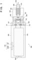
- Fig. 1 schematically shows the arrangement of an aerosol generation device 100 according to an embodiment.
- the aerosol generation device 100 can be configured to provide, to a user via an inhalation port 130, a gas containing an aerosol, a gas containing an aerosol and a flavor material, an aerosol, or an aerosol containing a flavor material in accordance with an operation requesting the aerosol (to be also referred to as an aerosol requesting operation hereinafter) such as an inhalation operation by the user.
- the aerosol generation device 100 can comprise a power supply unit 102 and an atomizer 104.
- the aerosol generation device 100 can comprise a holding portion 103 that detachably holds the atomizer 104.
- the power supply unit 102 may be understood as an inhalation unit controller.
- the atomizer 104 can be configured to atomize an aerosol source.
- the aerosol source can be, for example, a liquid such as a multivalent alcohol such as glycerin or propylene glycol. Alternatively, the aerosol source may contain a drug.
- the aerosol source can be a liquid, a solid, or a mixture of a liquid and a solid. A vapor source such as water may be used in place of the aerosol source.
- the aerosol generation device 100 may further comprise a capsule 106 containing a flavor source 131.
- the atomizer 104 can include a capsule holder 105 that detachably holds the capsule 106.
- the flavor source 131 can be a molded body obtained by molding, for example, a cigarette material. Alternatively, the flavor source 131 may be made of a plant (for example, mint, herb, Chinese medicine, coffee beans, or the like) except the cigarette. A fragrance such as menthol may be added to the flavor source.
- the flavor source 131 may be added to an aerosol source.
- the capsule holder 105 may be arranged in the power supply unit 102 in place of the atomizer 104.
- the atomizer 104 and the capsule holder 105 may be integrally formed in place of an arrangement in which the aerosol generation device 100 or the atomizer 104 includes the capsule holder 105.
- the power supply unit 102 can include electrical components 110.
- the electrical components 110 can include a user interface 116.
- the power supply unit 102 may be understood to include the electrical components 110 and the user interface 116.
- the user interface 116 can include a display unit DISP (for example, a light emitting element such as an LED (Light Emitting Diode) and/or an image display unit such as an LCD) and/or an operation unit OP (for example, a switch such as a button switch and/or a touch display).
- DISP for example, a light emitting element such as an LED (Light Emitting Diode) and/or an image display unit such as an LCD)
- an operation unit OP for example, a switch such as a button switch and/or a touch display.
- the holding portion 103 of the power supply unit 102 can include an electrical contact C1 and an electrical contact C2.
- the electrical contact C1 of the holding portion 103 can contact an electrical contact C3 of the atomizer 104
- the electrical contact C2 of the holding portion 103 can contact an electrical contact C4 of the atomizer 104.
- the power supply unit 102 can supply power to the atomizer 104 via the electrical contact C1 and the electrical contact C2.
- the atomizer 104 can include the electrical contact C3 and the electrical contact C4 described above.
- the atomizer 104 can include a heater HT for heating the aerosol source, a container 125 for holding the liquid aerosol source, and a transport portion 126 for transporting the aerosol source held by the container 125 to a heating region of the heater HT and holding the aerosol source in the heating region.
- the transport portion 126 is called a wick.
- At least part of the heating region of the heater HT can be arranged in a channel 128 formed in the atomizer 104.
- the electrical contact C1, the electrical contact C3, the heater HT, the electrical contact C4, and the electrical contact C2 form a current path for flowing the current to the heater HT.
- the transport portion 126 can be made of a fiber element such as a glass fiber, a porous material such as a ceramic, or a combination thereof. Note that the unit for transporting the aerosol source held in the container 125 to the heating region is not limited to the wick, but a spraying device such as a spray or a transporting unit such as a pump may be used instead.
- the atomizer 104 can include the capsule holder 105 for detachably holding the capsule 106.
- the capsule holder 105 can hold the capsule 106 such that part of the capsule 106 is accommodated in the capsule holder 105 or the atomizer 104 and the remaining part of the capsule 106 is exposed.
- the user can hold the inhalation port 130 with his/her mouth and suck the gas containing the aerosol. Since the detachable capsule 106 includes the inhalation port 130, the aerosol generation device 100 can be kept clean.
- the flavor material generated by the flavor source 131 is added to this aerosol, and the resultant material is transported to the inhalation port 130, thus allowing the user to suck the aerosol containing the flavor material. Since the flavor material generated by the flavor source 131 is added to the aerosol, the flavor material can be efficiently transported to the lungs of the user without staying in the oral cavity.
- the power supply unit 102 further includes a connector PG connected to an external device (not shown in Fig. 1 ).
- the external device connected to the power supply unit 102 can be, for example, a charger of the power supply unit 102.
- the external device functions as an external power supply for supplying power to the power supply unit 102.
- the external device may communicate with the power supply unit 102 via the connector PG.
- the atomizer 104 detachable from the power supply unit 102 includes the heater HT.
- the heater HT may be attached to the power supply unit 102 in place of the atomizer 104.
- an aerosol generation product including an aerosol base that holds the aerosol source and a filter may be exchangeably attached to the power supply unit 102.
- the aerosol generation product is inserted into the heater HT of the power supply unit 102, and accordingly the heater HT can heat the aerosol source in the aerosol base.
- the used aerosol generation product can be detachable from the power supply unit 102 in a state in which the heater HT is coupled to the power supply unit 102.
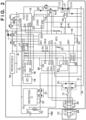
- Fig. 2 shows an example of the overall circuit arrangement of the power supply unit 102.
- the power supply unit 102 includes a plurality of circuit components shown in Fig. 2 .
- the outline of the arrangement of each circuit component will be described with reference to Fig. 2 , and then details of some circuit components will be described later with reference to other drawings.
- a controller 14 controls the overall operation of the power supply unit 102.
- the controller 14 can be a microcontroller unit formed by, for example, an integrated circuit (IC). More specifically, the controller 14 supplies a control signal to each circuit component in the power supply unit 102 to control the operation of each circuit component. In addition, the controller 14 controls power supply from an internal power supply BAT to the heater HT.
- IC integrated circuit
- the internal power supply BAT is a power supply for holding power supplied to the heater HT in order to heat the aerosol source.
- the internal power supply BAT can be formed by a primary battery such as a dry cell, a secondary battery such as a lithium ion battery, or a capacitor such as an electric double layer capacitor. In the following description, a case in which the internal power supply BAT is formed by the secondary battery will be described, unless otherwise specified.
- a connector 23 is a connector connectable to an external device CG.
- the external device CG includes a connector 24.
- the connector 23 of the power supply unit 102 is physically connected (coupled) to the connector 24 of the external device CG, the power supply unit 102 and the external device CG are electrically connected to each other.
- the connector 23 and the connector 24 can be connectable in a plurality of different directions.
- the external device CG can supply power to the internal power supply BAT via the connectors 23 and 24.
- the external device CG can communicate with each circuit component in the power supply unit 102.
- the external device CG and the power supply unit 102 perform I2C (Inter-Integrated Circuit) communication as a type of serial communication method.
- Each circuit component which performs communication in the power supply unit 102 includes a communication terminal ("SCL" in Fig. 2 ) for transmitting/receiving a clock signal and a communication terminal ("SDA" in Fig. 2 ) for transmitting/receiving a data signal.
- the clock signal communication terminals of the respective circuit components are connected to each other, and the data signal communication terminals of the respective circuit components are connected to each other.
- I2C communication is performed.
- another serial communication method such as UART (Universal Asynchronous Receiver/Transmitter) or SPI (Serial Peripheral Interface) may be used in place of the I2C communication.
- the external device CG can transmit data to the write terminal ("WRT" in Fig. 2 ) of the controller 14.
- the external device CG need not have a charging function, but can have only a communication function.
- the external device CG need not have the communication function, but may have only the charging function, or may have both the communication function and the charging function.
- the external device CG can be referred to as the external power supply. In the following description, a case in which the external device CG has both the charging function and the communication function will be described, unless otherwise specified.
- a polarity unification circuit BC is a circuit component for unifying the polarity of the connector 23.
- the polarity unification circuit BC is connected to the two power supply terminals of the connector 23.
- the polarity unification circuit BC connects a higher potential (for example, a power supply potential VBUS of the external device CG) to the positive electrode (via another electrical component) of the internal power supply BAT and a lower potential (for example, the ground potential of the external device CG) to the negative electrode (via another electrical component) of the internal power supply BAT.
- a fuse FS is arranged between the polarity unification circuit BC and the connector 23. If a current flowing between the polarity unification circuit BC and the connector 23 exceeds a threshold, the fuse FS is disconnected. Accordingly, power supply from the external device CG to the power supply unit 102 is stopped.
- a protection IC 16 is a circuit component for protecting the circuit components in the power supply unit 102 from an excessive current.
- the protection IC 16 is positioned on the power supply path for supplying power from the external device CG to the internal power supply BAT. If a current flowing through the protection IC 16 exceeds the threshold for a predetermined period, the protection IC 16 sets, to the disconnected state, the power supply path through which the current flows through the protection IC 16. Accordingly, the power supply from the external device CG to the power supply unit 102 is stopped to protect a subsequent circuit (for example, a transistor Q3).
- the protection IC 16 is connected to a ground line GL of the power supply unit 102.
- the ground line GL is connected to ground of a circuit board on which each circuit component (for example, the controller 14) of the power supply unit 102 is mounted. As a detailed example, ground of the circuit board is made of a metal plate.
- a transistor Q4 is a circuit component for preventing the flow of a current to the connector 23 during the power supply from the internal power supply BAT to the heater HT.
- the transistor Q4 can be an FET (Field Effect Transistor) or an IGBT (Insulated Gate type Bipolar Transistor).
- the transistor Q4 may be an n-channel MOS transistor. This also applies to other transistors to be described later.
- the transistor Q4 is positioned on the power supply path for supplying power from the external device CG to the internal power supply BAT.
- the transistor Q4 is arranged such that the direction from the external device CG to the internal power supply BAT is the forward direction of a parasitic diode of the transistor Q4.
- the gate of the transistor Q4 is connected to the controller 14.
- the transistor Q3 is a circuit component for adjusting the amount of power supplied from the external device CG to the internal power supply BAT.
- the protection IC 16 is positioned on the power supply path for supplying power from the external device CG to the internal power supply BAT.
- the transistor Q3 is positioned such that the direction from the external device CG to the internal power supply BAT is the reverse direction of the parasitic diode of the transistor Q3.
- the gate of the transistor Q3 is connected to the controller 14.
- a Schottky diode SD is connected parallel to the transistor Q3. More specifically, the cathode of the Schottky diode SD is connected to the source of the transistor Q3, and the anode of the Schottky diode SD is connected to the drain of the transistor Q3.
- a protection IC 17 is a circuit component for protecting the internal power supply BAT from the excessive current. More specifically, the protection IC 17 measures a voltage across a resistor RP connected to the negative electrode of the internal power supply BAT and determines a current flowing through the resistor RP. If this current exceeds a threshold, the protection IC 17 operates a transistor pair SP to stop the current flowing out from the negative electrode of the internal power supply BAT or the current flowing in the negative electrode.
- a voltage converter 13 is a circuit component for converting the power supply voltage supplied from the internal power supply BAT into a heater driving voltage.
- the power supply voltage from the internal power supply BAT is supplied to the input terminal ("VIN” in Fig. 2 ) of the voltage converter 13, and the heater driving voltage is output from the output terminal ("VOUT” in Fig. 2 ) of the voltage converter 13.
- An enable signal is supplied from the enable terminal ("EN” in Fig. 2 ) of the voltage converter 13 to the control terminal ("EN2" in Fig. 2 ) of the controller 14.
- the ground terminal (“GND” in Fig. 2 ) of the voltage converter 13 is connected to the ground line GL.
- the voltage converter 13 can communicate with the controller 14 by the I2C communication.
- the voltage converter 13 may be formed by a DC/DC converter.
- the voltage converter 13 may be formed by a buck-boost DC/DC converter.
- the output terminal of the voltage converter 13 is connected to the heater HT via a transistor Q1.
- the gate of the transistor Q1 is connected to the controller 14.
- the controller 14 switches the level of the control signal supplied to the gate of the transistor Q1 to switch ON/OFF state of the transistor Q1. During the ON period of the transistor Q1, the heater driving voltage is applied to the heater HT to heat the heater HT.
- a regulator 12 is a circuit component for converting the power supply voltage supplied from the internal power supply BAT into a power supply voltage of an operational amplifier 15.
- the power supply voltage of the operational amplifier 15 is used also to measure the resistance value of the heater HT.
- the regulator 12 can be a linear regulator, and more specifically a low dropout (LDO) regulator.
- the power supply voltage is supplied from the internal power supply BAT to the input terminal ("IN” in Fig. 2 ) of the regulator 12.
- the power supply voltage of the operational amplifier 15 is output from the output terminal ("OUT" in Fig. 2 ) of the regulator 12.
- An enable signal is supplied from the control terminal (“EN2" in Fig. 2 ) of the controller 14 to the enable terminal ("EN” in Fig. 2 ) of the regulator 12.
- the ground terminal (“GND” in Fig. 2 ) of the regulator 12 is connected to the ground line GL.
- the enable terminal of the voltage converter 13 and the enable terminal of the regulator 12 are connected to the common control terminal ("EN2" in Fig. 2 ) of the controller 14.
- the controller 14 may have individual control terminals respectively connected to the enable terminal of the voltage converter 13 and the enable terminal of the regulator 12.
- the voltage output from the output terminal of the regulator 12 may be kept constant.
- the output terminal of the regulator 12 is connected to the heater HT via a diode BE, a transistor Q2, and a resistor Rs.
- the diode BE prevents the reverse flow of the current from the transistor Q2 to the regulator 12.
- the gate of the transistor Q2 is connected to the controller 14.
- the controller 14 switches the level of the control signal supplied to the gate of the transistor Q2 to switch the ON/OFF state of the transistor Q2. During the ON period of the transistor Q2, the output voltage of the regulator 12 is applied to the heater HT.
- the node between the transistor Q2 and the resistor Rs is connected to the ground line GL via the resistor R2 and the resistor R1.
- the controller 14 is connected to the node between the resistor R2 and the resistor R1.
- the noninverting input terminal of the operational amplifier 15 is connected to one terminal of the heater HT.
- the inverting input terminal of the operational amplifier 15 is connected to the other terminal of the heater HT.
- the output terminal of the operational amplifier 15 is connected to the controller 14.
- the operational amplifier 15 supplies the voltage applied to the heater HT to the controller 14. If the heater HT has a positive or negative temperature coefficient characteristic by which the resistance value changes depending on the temperature of the heater HT, the voltage applied to the heater HT has a strong correlation with the temperature of the heater HT.
- the controller 14 estimates the temperature of the heater HT based on this voltage, adjusts the amount of power supplied to the heater HT based on this estimated temperature, and controls the temperature of the heater HT based on the adjusted amount of power.
- a voltage obtained by dividing a predetermined voltage output from the regulator 12 by the resistor Rs and the heater HT is input to the noninverting input terminal of the operational amplifier 15. Since this divided voltage has a strong correlation with the temperature of the heater HT, the controller 14 can accurately estimate the temperature of the heater HT from the voltage (the signal) output from the output terminal of the operational amplifier 15.
- a regulator 11 is a circuit component for converting the voltage supplied from the external device CG or the internal power supply BAT into power supply voltages of a switch unit 20, a puff sensor 21, and a touch sensor 22.
- the voltage output from the regulator 11 is also used as the power supply voltage of the I2C communication.
- the regulator 11 can be a linear regulator.
- the power supply voltage is supplied from the external device CG or the internal power supply BAT to the input terminal of the regulator 11, and the power supply voltage of each circuit component is output from the output terminal of the regulator 11.
- the power supply voltages of an LED driver 18 and an LED 19 are not supplied from the output terminal of the regulator 11, as will be described later.
- the power supply voltages of the LED driver 18 and the LED 19 may be supplied from the output terminal of the regulator 11.
- An enable signal is supplied from the control terminal ("EN1" in Fig. 2 ) of the controller 14 to the enable terminal of the regulator 11.
- the ground terminal of the regulator 11 is connected to the ground line GL.
- the regulator 11 can be used in both a case in which the power is supplied from the external device CG and a case in which the internal power supply BAT is discharged.
- the regulator 12 is not used.
- the regulator 12 is used.
- the regulator 11 can be a power-saving component as compared with the regulator 12.
- the regulator 12 generates the operation voltage of the operational amplifier 15.
- the operation voltage of the operational amplifier 15 influences the accuracy and speed of temperature estimation of the heater HT by the controller 14.
- the regulator 12 can be a component having responsiveness higher than that of the regulator 11.
- the LED driver 18 is a circuit component for controlling the operation of the LED 19.
- the LED 19 is equivalent to a display unit DISP in Fig. 1 .
- the power supply voltage is supplied from the external device CG or the internal power supply BAT to the power supply terminal of the LED driver 18.
- the ground terminal of the LED driver 18 is connected to the ground line GL.
- the LED driver 18 can communicate with the controller 14 by the I2C communication.
- the LED driver 18 changes the ON state of the LED 19 to notify the user of the state of the aerosol generation device 100. More specifically, the LED driver 18 changes the state of the LED 19 as the ON state, the OFF state, or the flickering state. If the LED 19 includes a plurality of LEDs, the number of ON LEDs can be increased/decreased.
- the switch unit 20 is a circuit component for changing the state of the communication path of the I2C communication between the connector 23 and the controller 14 to the disconnected state or the conductive state.
- the power supply voltage is supplied from the regulator 11 to the power supply terminal of the switch unit 20.
- the ground terminal of the switch unit 20 is connected to the ground line GL.
- the enable terminal (“EN" in Fig. 2 ) of the switch unit 20 is connected to the node between a resistor R4 and a resistor R3.
- the resistor R4 and the resistor R3 are connected in series with each other between the line for receiving the power supply voltage from the external device CG and the ground line GL.
- the node between the resistor R4 and the resistor R3 is set at high level while the power supply voltage is supplied from the external device CG.
- This node is also connected to the detection terminal ("VBUS" in Fig. 2 ) of the controller 14.
- the controller 14 can detect that the fact that the power supply voltage is supplied from the external device CG. If the voltage applied to the enable terminal is set at high level, the switch unit 20 sets the communication path of the I2C communication between the connector 23 and the controller 14 to the conductive state. On the other hand, if the voltage applied to the enable terminal is set at low level, the switch unit 20 sets the communication path of the I2C communication between the connector 23 and the controller 14 to the disconnected state. Accordingly, even if static electricity is applied to the communication terminal of the connector 23 or the communication terminal is short-circuited, an unexpected current will not flow to the circuit component in the power supply unit 102. Therefore, the safety of the power supply unit 102 can be improved.
- the puff sensor 21 is a circuit component for detecting the inhalation operation of the user.
- the puff sensor 21 is formed by a microphone condenser, a flow rate sensor, or one or more pressure sensors.
- the power supply voltage is supplied from the regulator 11 to the power supply terminal of the puff sensor 21.
- the ground terminal of the puff sensor 21 is connected to the ground line GL.
- the puff sensor 21 can communicate with the controller 14 by the I2C communication.
- the touch sensor 22 is a circuit component for detecting the touch operation by the user.
- the power supply voltage is supplied from the regulator 11 to the power supply terminal of the touch sensor 22.
- the ground terminal of the touch sensor 22 is connected to the ground line GL.
- the touch sensor 22 notifies the controller 14 of the detection result of the touch operation.
- a temperature sensor TM is a circuit component for measuring the temperature near the internal power supply BAT.
- the temperature sensor TM can be formed by a thermistor, a thermocouple, a temperature measurement resistor band, or an IC temperature sensor.
- the controller 14 applies a voltage from the output terminal ("VO" in Fig. 2 ) to the temperature sensor TM. This voltage is divided by the resistor R5 and the temperature sensor TM and input to the input terminal ("VI" in Fig. 2 ) of the controller 14.
- the controller 14 measures the potential at the input terminal to determine the resistance value of the temperature sensor TM, and determines the temperature of the temperature sensor TM based on this resistance value. If the temperature sensor TM is arranged on or near the surface of the internal power supply BAT, the temperature of the temperature sensor TM can be used as the temperature of the internal power supply BAT.
- the controller 14 measures a voltage across a resistor RD connected to the negative electrode of the internal power supply BAT to determine a current flowing through the resistor RD. If this current exceeds a threshold, the controller 14 operates the transistor Q3 or the voltage converter 13 to stop a current flowing out from the negative electrode of the internal power supply BAT or a current flowing into the negative electrode. Note that by the internal processing of the controller 14, the current flowing out from the negative electrode of the internal power supply BAT and the current flowing into the negative electrode of the internal power supply BAT have positive values. If the current exceeds the threshold and the current flowing out from the negative electrode of the internal power supply BAT or flowing into the negative electrode is stopped, the controller 14 can improve the safety of the aerosol generation device 100.
- controller 14 may stop the current flowing into the negative electrode of the internal power supply BAT by operating the transistor Q1 or stop the current flowing into the negative electrode of the internal power supply BAT by operating the voltage converter 13 and the transistor Q1.
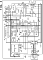
- the external device CG supplies the power supply potential VBUS to one of the two power supply terminals of the connector 23 of the power supply unit 102 and supplies the ground potential to the other power supply terminal.
- the ground potential is obtained from ground (not shown) provided in the external device CG.
- the current flowing from the power supply terminal on the high potential side of the connector 23 sets the potential of a node N1 to high level via the polarity unification circuit BC and the protection IC 16.
- the node N1 is a node to which the protection IC 16, the drain of the transistor Q4, and the resistor R4 are connected.
- a current flows through the parasitic diode of the transistor Q4 in the forward direction, so that a node N2 is also set at high level.
- the node N2 is a node to which the source of the transistor Q4, the source of the transistor Q3, and the cathode of the Schottky diode SD are connected.
- the transistor Q3 since the transistor Q3 is kept off, the current does not flow over the transistor Q3. In other words, at this stage, the internal power supply BAT is not charged.
- a current flows from the node N1 to the ground line GL via the resistor R4 and the resistor R3, so that a node N3 is also set at high level.
- the node N3 is a node to which the resistor R4, the resistor R3, the enable terminal of the switch unit 20, and the detection terminal of the controller 14 are connected.
- a high-level signal (the voltage signal) is simultaneously supplied to the enable terminal of the switch unit 20 and the detection terminal of the controller 14. That is, the enable terminal of the switch unit 20 is automatically set at high level when the power supply potential is supplied from the external device CG to the power supply terminal of the connector 23.
- the node N2 is connected to the power supply terminal of the controller 14, the input terminal of the regulator 11, and the power supply terminal of the LED driver 18, and also to the power supply terminal of the LED 19.
- the operation voltages are supplied to the controller 14, the LED driver 18, and the LED 19, thereby activating these circuit components.
- the activated controller 14 supplies a high-level signal to the enable terminal of the regulator 11. Accordingly, the regulator 11 supplies the operation voltages to the power supply terminal of the switch unit 20, the power supply terminal of the puff sensor 21, and the power supply terminal of the touch sensor 22.
- the switch unit 20 Upon reception of the operation voltage by the switch unit 20, since the level at the enable terminal is high level, the switch unit 20 sets the communication path between the connector 23 and the controller 14 to a conductive state. This makes it possible to cause the controller 14 to communicate with the external device CG. Since the communication path between the connector 23 and the controller 14 is set at the conductive state if needed, generation of an abnormality through this communication path can be suppressed. In addition, the controller 14 can also communicate with the LED driver 18 and the puff sensor 21.
- a current flows from the node N3 to the positive electrode of the internal power supply BAT.
- This current charges the internal power supply BAT. More specifically, power is supplied from the external device CG to the internal power supply BAT via a power supply path 301 passing in the order of the fuse FS, the polarity unification circuit BC, the protection IC 16, the transistor Q4, and the transistor Q3 from the connector 23 to the internal power supply BAT.
- the current flowing out from the negative electrode of the internal power supply BAT flows from the power supply terminal of the connector 23 on the low potential side to ground of the external device CG via a power supply path 302.
- the power supply path 302 passes from the negative electrode of the internal power supply BAT to the connector 23 in the order of the resistor RP, the transistor pair SP, the resistor RD, and the polarity unification circuit BC.
- the controller 14 can control the voltage of the gate of the transistor Q3 to supply power from the external device CG to the internal power supply BAT.
- the transistor Q3 is also called a charging transistor.
- the transistor Q3 controlled by the dropper method discards an unnecessary component of the power supplied from the connector 23 as heat, thereby generating the voltage and current used for charging of the internal power supply BAT.
- the controller 14 may be configured to acquire the current and voltage supplied to the transistor Q3.
- the controller 14 may feed back, to the control of the dropper method, a difference between the acquired current and voltage and the voltage and current to be used for charging of the internal power supply BAT, thereby improving the accuracy of the charging of the internal power supply BAT.
- a charging integrated circuit is unnecessary, thereby reducing the circuit scale.
- the controller 14 can acquire the state of the internal power supply BAT.
- the state of the internal power supply BAT includes at least one of the temperature of the internal power supply BAT and the state of health (SOH) of the internal power supply BAT.
- the temperature of the internal power supply BAT and the state of health of the internal power supply BAT may be determined based on the temperature of the temperature sensor TM or a time required for charging.
- the temperature of the internal power supply BAT and the state of health of the internal power supply BAT may be acquired by a dedicated IC and acquired by the controller 14 by the I2C communication from the dedicated IC.
- the controller 14 can change at least one of the drain current and thee drain voltage of the transistor Q3 based on the state of the internal power supply BAT and adjust the power supplied from the external device CG to the internal power supply BAT. This makes it possible for the controller 14 to control the charging of the internal power supply BAT with a larger degree of freedom.
- the parasitic diode of the transistor Q4 is arranged on a path between the polarity unification circuit BC and the positive electrode of the internal power supply BAT.
- the forward direction of the parasitic diode of the transistor Q4 is a direction from the polarity unification circuit BC to the positive electrode of the internal power supply BAT.
- the potential (that is, the power supply potential VBUS) of the node N1 is reduced by the forward voltage of (the parasitic diode of) the transistor Q4, and the reduced potential is supplied to the transistor Q3.
- the transistor Q3 controlled by the dropper method discards an unnecessary component of the power supplied from the connector 23 as heat, thereby generating the voltage and current used for charging of the internal power supply BAT.
- the transistor Q4 If power appropriately reduced by (the parasitic diode of) the transistor Q4 can be supplied to the transistor Q3, heat generated when the transistor Q3 generates the voltage for charging the internal power supply BAT can be reduced. In addition, the heat generated at the time of charging in the power supply unit 102 can be dispersed to the transistor Q3 and the transistor Q4. This makes it possible to improve durability of the transistor Q3 and the power supply unit 102.
- a diode may be used in place of the transistor Q4.
- the forward voltage of the parasitic diode of the transistor Q4 is higher than the forward voltage of the diode, the potential supplied to the transistor Q3 can be efficiently reduced by using the parasitic diode of the transistor Q4.
- the negative electrode of the internal power supply BAT is not connected to the ground line GL (that is, ground of the power supply unit 102). For this reason, the current from the negative electrode of the internal power supply BAT flows to ground of the external device CG via the connector 23.
- the resistor RP and the resistor RD are connected in series with each other on the power supply path 302.
- the current flowing out from the negative electrode of the internal power supply BAT at the time of charging of the internal power supply BAT passes through the resistor RP and the resistor RD.
- the protection IC 17 measures a voltage across the resistor RP and determines the value of the current flowing through the resistor RP based on the measured voltage.
- the current flowing out from the negative electrode of the internal power supply BAT and the current flowing into the negative electrode of the internal power supply BAT indicate positive values by processing in the protection IC 17. Based on this current value, the protection IC 17 stops supplying power from the external device CG to the internal power supply BAT. For example, when this current exceeds the threshold, the protection IC 17 turns off one or both transistors of the transistor pair SP, the current flowing through the power supply path 302 may be cut off.
- the controller 14 measures a voltage across the resistor RD and determines the value of the current flowing through the resistor RD based on the measured voltage. As described above, by the processing in the controller 14, the current flowing out from the negative electrode of the internal power supply BAT and the current flowing into the negative electrode of the internal power supply BAT indicate the positive values. The controller 14 stops supply of the power from the external device CG to the internal power supply BAT based on this current value. For example, when this current value exceeds the threshold, the controller 14 may turn off the transistor Q3, thereby cutting off the current flowing through the power supply path 301. In this manner, when the current flowing through the power supply path 302 is monitored by both of the protection IC and the controller 14, the safety of the power supply unit 102 is further improved. Instead, only one of the resistor RP and the resistor RD may be arranged on the power supply path 302.
- the controller 14 instructs to stop the supply of the power supply potential to the external device CG by the I2C communication.
- the controller 14 keeps the transistor Q3 off even if the power supply potential is supplied from the external device CG.
- the time of excessive discharging of the internal power supply BAT indicates the time when the voltage of the internal power supply BAT is lower than the discharge end voltage and the voltage for operating the controller 14 cannot be supplied to the power supply terminal of the controller 14. In other words, at the time of excessive discharging, the controller 14 cannot be operated by only the power supplied from the internal power supply BAT.
- the power supply path 305 is a path passing from the connector 23 in the order of the fuse FS, the polarity unification circuit BC, the protection IC 16, and the transistor Q4.
- the power supply path 305 does not pass the transistor Q3.
- the operation power is supplied from the external device CG to the power supply terminal of the switch unit 20 via a power supply path 304. More specifically, since the controller 14 cannot be operated at the time of excessive discharging of the internal power supply BAT, the enable signal is not supplied from the control terminal ("EN1" in Fig.
- the controller 14 can supply the enable signal from the control terminal to the enable terminal of the regulator 11.
- the operation power is also supplied from the external device CG to the input terminal of the regulator 11 via the power supply path 304. Accordingly, the operation power is supplied from the regulator 11 to the power supply terminal of the switch unit 20.
- the power supply path 304 is a path passing from the connector 23 in the order of the fuse FS, the polarity unification circuit BC, the protection IC 16, the transistor Q4, and the regulator 11 and does not pass through the transistor Q3.
- the high-level signal is supplied to the enable terminal of the switch unit 20. Accordingly, even if the transistor Q3 is kept off, the controller 14 can communicate with the external device CG, and for example, an error state can be transmitted. In addition, even if the transistor Q3 is kept off, since the power is supplied from the regulator 11 to the LED driver 18, the controller 14 uses the LED 19 to notify the user of the error.
- the controller 14 controls the transistor Q3 to restore the internal power supply BAT from the excessive discharging state. Even in this state, the controller 14 can control the transistor Q3 in accordance with the dropper method. Note that before at least the voltage of the internal power supply BAT is equal to or higher than the discharge end voltage, the controller 14 may control the transistor Q3 so that the voltage and current supplied to the internal power supply BAT are lower and smaller than those in the normal operation. Note that as a detailed example, the normal operation indicates the time when the voltage of the internal power supply BAT is equal to or higher than the discharge end voltage.
- the current flowing out from the positive electrode of the internal power supply BAT is supplied to the power supply terminal of the controller 14 via the power supply path 403 passing in the order of a node N4, the Schottky diode SD, and the node N2.
- the controller 14 receives the operation power. Since the forward resistance of the Schottky diode SD is lower than the forward resistance of the transistor Q3, the current mainly flows in the Schottky diode SD from the node N4 to the node N2.
- the Schottky diode SD By arranging the Schottky diode SD in this manner, the power can be supplied to the controller 14 with a higher efficiency (that is, a low loss) than a case in which the current flows to the parasitic diode of the transistor Q3.
- the node N2 is also connected to the input terminal of the regulator 11, the power supply terminal of the LED driver 18, and the power supply terminal of the LED 19.
- the operation power is supplied to each of the LED driver 18 and the LED 19.
- the controller 14 supplies the high-level signal to the enable terminal of the regulator 11. Accordingly, the regulator 11 supplies the operation power to each of the power supply terminal of the switch unit 20, the power supply terminal of the puff sensor 21, and the power supply terminal of the touch sensor 22.
- the parasitic diode of the transistor Q4 is arranged on a path between the node N2 and the connector 23.
- the reverse direction of the parasitic diode of the transistor Q4 is a direction from the node N2 to the connector 23. For this reason, no current flows from the node N2 to the connector 23.
- the parasitic diode of the transistor Q4 functions as a reverse flow prevention element. That is, the transistor Q4 serves as the reverse flow prevention element and also serves as an element for suppressing heating of the transistor Q3 at the time of charging.
- the transistor Q4 is an element for suppressing the concentration of heat in the power supply unit 102 at the time of charging.
- the switch unit 20 sets the communication path between the connector 23 and the controller 14 to the disconnected state.
- the communication terminal of the connector 23 is set in a state in which the communication terminal of the controller 14 is disconnected from the communication terminal of another circuit component (for example, the puff sensor 21). For this reason, even if static electricity is applied to the communication terminal of the connector 23 or the communication terminal is short-circuited, no unexpected current flows in the circuit components in the power supply unit 102. Therefore, the safety of the power supply unit 102 can be improved.
- the controller 14 can communicate with another circuit component (for example the puff sensor 21) in the power supply unit 102. That is, in both a case in which the communication path between the connector 23 and the controller 14 is set in the conductive state and a case in which this communication path is set in the disconnected state, the communication terminal of the controller 14 and the communication path of another integrated circuit (for example, the puff sensor 21) are set in the conductive state.
- another switch unit may be arranged in the communication path between the controller 14 and the other integrated circuit, and the state may be switched independently of the communication path between the connector 23 and the controller 14.
- the controller 14 When heating the heater HT, the controller 14 turns on the transistor Q1. Accordingly, a current flows from the positive electrode of the internal power supply BAT to the heater HT via a power supply path 401.
- the power supply path 401 is a path from the positive electrode of the internal power supply BAT to the electrical contact C1 via the voltage converter 13.
- the power supply path 401 does not pass through the transistor Q3. Accordingly, since a decrease in power supplied from the internal power supply BAT to the heater HT can be suppressed, high-efficiency aerosol generation is possible.
- the voltage converter 13 is formed by a boost DC/DC converter or a buck-boost DC/DC converter, a higher voltage can be supplied to the heater HT. The amount of aerosol to be generated can be increased.
- the current passing through the heater HT flows into the negative electrode of the internal power supply BAT via the power supply path 402.
- the power supply path 402 is a path from the electrical contact C2 to the negative electrode of the internal power supply BAT via the resistor RD, the transistor pair SP, and the resistor RP. Since the negative electrode of the internal power supply BAT is not connected to the ground line GL, the current passing through the heater HT passes through the resistor RD and the resistor RP as described above.
- the protection IC 17 measures a voltage across the resistor RP to determine the value of a current flowing through the resistor RP based on the measured voltage.
- the protection IC 17 stops the supply of the power from the internal power supply BAT to the heater HT based on this current value. For example, if this current value exceeds the threshold, the protection IC 17 turns off both the transistors of the transistor pair SP, and the current flowing through the power supply path 402 can be cut off.
- the controller 14 measures a voltage across the resistor RD to determine the value of a current flowing through the resistor RD based on the measured voltage.
- the controller 14 stops the supply of power from the internal power supply BAT to the heater HT based on this current value. For example, if this current value exceeds the threshold, the controller 14 turns off the transistor Q1 and/or stops supplying the enable signal from the control terminal ("EN2" in Fig. 2 ) to the enable terminal ("EN" in Fig. 2 ) of the voltage converter 13, the controller 14 cuts off the current flowing through the power supply path 401. In this manner, when the current flowing through the power supply path 302 is monitored by both the protection IC and the controller 14, the safety of the power supply unit 102 can be further improved. Instead, only one of the resistor RP and the resistor RD may be arranged on the power supply path 402.
- the resistor RP and the resistor RD are arranged in the common portion between the power supply path 302 and the power supply path 402. Instead, at least one of the resistor RP and the resistor RD may be arranged to pass through only one of the power supply path 302 and the power supply path 402. In addition, the power supply unit 102 need not monitor the current passing through the resistor RP and the resistor RD. In addition, the resistor RP or the resistor RD may be arranged in the power supply path 401. On the other hand, as in the embodiment shown in Fig.
- each of the protection IC 17 and the controller 14 may include an operational amplifier for acquiring the voltage applied to the resistor RP and the resistor RD.
- the transistor Q4 may be located at another position.
- the transistor Q4 may be arranged between the polarity unification circuit BC and the protection IC 16.
- the protection IC 16 may be located at another position.
- the protection IC 16 may be arranged between the node N1 and the transistor Q4.
- the polarity unification circuit BC and the connector 23 will be described in detail with reference to Figs. 5A and 5B . Some circuit components in Fig. 2 are not illustrated in Figs. 5A and 5B .
- the connector 23 of the power supply unit 102 can be connected to the external device CG (more specifically, its connector 24).
- the connector 23 includes a write terminal 501, two power supply terminals 502 and 503, and four communication terminals 504 to 507.
- the write terminal 501 is a terminal used to cause the external device CG to write data in the controller 14 of the power supply unit 102.
- the power supply terminals 502 and 503 are terminals used to cause the power supply unit 102 to receive supply of the power from the external device CG.
- the communication terminals 504 to 507 are terminals used to cause the controller 14 of the power supply unit 102 to communicate with the external device CG. As described above, in some embodiments, communication between the power supply unit 102 and the external device CG is performed by the I2C communication.
- the communication terminals 504 and 505 are used to communicate the clock signal in the I2C communication.
- the communication terminals 506 and 507 are used to communicate the data signal in the I2C communication.
- the write terminal 501 of the connector 23 is connected to a write terminal 553 of the controller 14. Both the power supply terminals 502 and 503 of the connector 23 are connected to the polarity unification circuit BC.
- the communication terminals 504 and 505 of the connector 23 are connected to a terminal 541 of the switch unit 20. Both the communication terminals 506 and 507 of the connector 24 are connected to a terminal 542 of the switch unit 20.
- a terminal 543 of the switch unit 20 is connected to the communication terminal 551 of the controller 14.
- a terminal 544 of the switch unit 20 is connected to the communication terminal 552 of the controller 14.
- the switch unit 20 includes a switch 546 connected between the terminal 541 and the terminal 543 and a switch 547 connected between the terminal 542 and the terminal 544.
- the switch 546 is set ON, the path between the terminal 541 and the terminal 543 is set in the conductive state.
- the switch 546 is set OFF, the path between the terminal 541 and the terminal 543 is set in the disconnected state.
- the switch 547 is set ON, the path between the terminal 542 and the terminal 544 is set in the conductive state.
- the switch 547 When the switch 547 is set OFF, the path between the terminal 542 and the terminal 544 is set in the disconnected state.
- the switch unit 20 When a high-level signal is input to the enable terminal EN, the switch unit 20 turns on the switches 546 and 547.
- a low -level signal is input to the enable terminal EN, the switch unit 20 turns off the switches 546 and 547.
- a communication path 571 for communicating the clock signal is formed between the communication terminal 504 of the connector 23 and a communication terminal 551 of the controller 14. Since the switch 546 is positioned on this communication path 571, if the switch 546 is turned on, the communication path 571 is set in the conductive state. If the switch 546 is turned off, the communication path 571 is set in the disconnected state. Of the communication path 571, the communication terminal 505 of the connector 23 is connected to a node 536 between the communication terminal 504 of the connector 23 and the switch 546. Therefore, the clock signal transmitted from the communication terminal 551 of the controller 14 is output from both the communication terminal 504 and the communication terminal 505 of the connector 23.
- a communication path 572 for communicating the data signal is formed between the communication terminal 506 of the connector 23 and a communication terminal 552 of the controller 14. Since the switch 547 is positioned on this communication path 572, if the switch 547 is turned on, the communication path 572 is set in the conductive state. If the switch 547 is turned off, the communication path 572 is set in the disconnected state. Of the communication path 572, the communication terminal 507 of the connector 23 is connected to a node 535 between the communication terminal 506 of the connector 23 and the switch 547. Therefore, the data signal transmitted from the communication terminal 552 of the controller 14 is output from both the communication terminal 506 and the communication terminal 507 of the connector 23.
- the connector 24 of the external device CG includes a write terminal 511, two power supply terminals 512 and 513, and four communication terminals 514 to 517.
- the write terminal 511 is a terminal used to cause the external device CG to write data in the controller 14 of the power supply unit 102.
- the write terminal 511 is connected to a write terminal 583 of a controller 580 of the external device CG.
- the power supply terminals 512 and 513 are terminals used to cause the external device CG to supply power to the power supply unit 102.
- the external device CG (more specifically, its voltage generation circuit 590) supplies the power supply potential to the power supply terminal 512.
- the power supply terminal 513 is connected to ground of the external device CG.
- the communication terminals 514 to 517 are terminals used to cause the external device CG to communicate with the controller 14 of the power supply unit 102.
- the communication terminals 514 and 515 are used to communicate the clock signal in the I2C communication.
- the communication terminals 516 and 517 are used to communicate the data signal in the I2C communication.
- Both the communication terminals 514 and 515 of the connector 24 are connected to a communication terminal 581 of the controller 580 of the external device CG.
- Both the communication terminals 516 and 517 of the connector 24 are connected to a communication terminal 582 of the controller 580 of the external device CG.
- the connector 23 and the connector 24 can be connected in two different directions. More specifically, the connector 23 and the connector 24 are connectable in a direction indicated in Fig. 5A and a direction indicated in Fig. 5B .
- the direction of the connector 24 in Fig. 5B is a direction 180° rotated from the direction of the connector 24 in Fig. 5A .
- the respective terminals of the two connectors are connected indicated by broken lines in Fig. 5A . More specifically, the write terminal 501 is connected to the write terminal 511, the power supply terminal 502 is connected to the power supply terminal 512, the power supply terminal 503 is connected to the power supply terminal 513, the communication terminal 504 is connected to the communication terminal 514, the communication terminal 505 is connected to the communication terminal 515, the communication terminal 506 is connected to the communication terminal 516, and the communication terminal 507 is connected to the communication terminal 517.
- the power supply potential is supplied to the power supply terminal 502 of the connector 23, and the ground potential is supplied to the power supply terminal 503 of the connector 23.
- the respective terminals of the two connectors are connected as indicated by the broken lines in Fig. 5B .
- the write terminal 501 is connected to the write terminal 511
- the power supply terminal 502 is connected to the power supply terminal 513
- the power supply terminal 503 is connected to the power supply terminal 512
- the communication terminal 504 is connected to the communication terminal 515
- the communication terminal 505 is connected to the communication terminal 514
- the communication terminal 506 is connected to the communication terminal 517
- the communication terminal 507 is connected to the communication terminal 516.
- the power supply potential is supplied to the power supply terminal 503 of the connector 23, and the ground potential is supplied to the power supply terminal 502 of the connector 23.
- the write terminal 501 is positioned at the center of the connector 23 and the write terminal 511 is positioned at the center of the connector 24, the write terminal 501 and the write terminal 511 are connected regardless of the direction of connecting the connector 23 and the connector 24. For this reason, the data output from the write terminal 511 of the controller 580 of the external device CG is written in the write terminal 553 of the controller 14 of the power supply unit 102 regardless of the direction of connecting the connector 23 and the connector 24. As described above, when the terminals are located at the centers of the connectors 23 and 24, the number of terminals required to allow connection in the plurality of directions can be reduced.
- All the communication terminals 504 and 505 of the connector 23 and the communication terminals 514 and 515 of the connector 24 are used for communicating the clock signal. Regardless of the direction of connecting the connector 23 and the connector 24, the clock signal is communicated between the communication terminal 581 of the controller 580 of the external device CG and the communication terminal 551 of the controller 14 of the power supply unit 102. All the communication terminals 506 and 507 of the connector 23 and the communication terminals 516 and 517 of the connector 24 are used for communicating the data signal. Regardless of the direction of connecting the connector 23 and the connector 24, the data signal is communicated between the communication terminal 582 of the controller 580 of the external device CG and the communication terminal 552 of the controller 14 of the power supply unit 102.
- each of the connector 23 and the connector 24 includes two communication terminals used to communicate the clock signal and two communication terminals used to communicate the data signal.
- one of the connector 23 and the connector 24 may include one communication terminal used to communicate the clock signal and/or one communication terminal used to communicate the data signal.
- the communication terminal 504 is connected to the communication terminal 514 if the connector 23 and the connector 24 are connected in the direction indicated in Fig. 5A . If the connector 23 is connected to the connector 24 in the direction indicated in Fig. 5B , the communication terminal 504 is connected to the communication terminal 515. If the connector 23 includes only the communication terminal 505 as the communication terminal used to communicate the clock signal, the communication terminal 505 is connected to the communication terminal 515 if the connector 23 and the connector 24 are connected in the direction indicated in Fig. 5A . If the connector 23 is connected to the connector 24 in the direction indicated in Fig. 5B , the communication terminal 505 is connected to the communication terminal 514.
- the communication terminal 506 is connected to the communication terminal 516 if the connector 23 and the connector 24 are connected in the direction indicated in Fig. 5A . If the connector 23 is connected to the connector 24 in the direction indicated in Fig. 5B , the communication terminal 506 is connected to the communication terminal 517. If the connector 23 includes only the communication terminal 507 as the communication terminal used to communicate the data signal, the communication terminal 506 is connected to the communication terminal 517 if the connector 23 and the connector 24 are connected in the direction indicated in Fig. 5A . If the connector 23 is connected to the connector 24 in the direction indicated in Fig. 5B , the communication terminal 507 is connected to the communication terminal 516.
- the connector 23 includes one communication terminal used to communicate the clock signal and/or the communication terminal used to communicate the data signal
- the connector 24 includes two communication terminals used to communicate the clock signal and/or two communication terminals used to communicate the data signal, the communication is possible between the controller 580 of the external device CG and the controller 14 of the power supply unit 102 regardless of the direction of connecting the connector 23 and the connector 24.
- the communication terminal 514 is connected to the communication terminal 504 if the connector 23 and the connector 24 are connected in the direction indicated in Fig. 5A . If the connector 23 is connected to the connector 24 in the direction indicated in Fig. 5B , the communication terminal 514 is connected to the communication terminal 505. If the connector 23 includes only the communication terminal 515 as the communication terminal used to communicate the clock signal, the communication terminal 515 is connected to the communication terminal 505 if the connector 23 and the connector 24 are connected in the direction indicated in Fig. 5A . If the connector 23 is connected to the connector 24 in the direction indicated in Fig. 5B , the communication terminal 515 is connected to the communication terminal 504.
- the communication terminal 516 is connected to the communication terminal 506 if the connector 23 and the connector 24 are connected in the direction indicated in Fig. 5A . If the connector 23 is connected to the connector 24 in the direction indicated in Fig. 5B , the communication terminal 516 is connected to the communication terminal 507. If the connector 23 includes only the communication terminal 517 as the communication terminal used to communicate the data signal, the communication terminal 517 is connected to the communication terminal 507 if the connector 23 and the connector 24 are connected in the direction indicated in Fig. 5A . If the connector 23 is connected to the connector 24 in the direction indicated in Fig. 5B , the communication terminal 517 is connected to the communication terminal 506.
- the connector 24 includes one communication terminal used to communicate the clock signal and/or the communication terminal used to communicate the data signal, and if the connector 23 includes two communication terminals used to communicate the clock signal and/or two communication terminals used to communicate the data signal, the communication is possible between the controller 580 of the external device CG and the controller 14 of the power supply unit 102 regardless of the direction of connecting the connector 23 and the connector 24.
- the polarity unification circuit BC includes four diodes 521 to 524 and four nodes 531 to 534.
- the node 531 is connected to the cathode of the diode 521 and the cathode of the diode 522.
- the node 534 is connected to the anode of the diode 523 and the anode of the diode 524.
- the node 532 is connected to the power supply terminal 502 of the connector 23, the anode of the diode 521, and the cathode of the diode 523.
- the node 533 is connected to the power supply terminal 503 of the connector 23, the anode of the diode 522, and the cathode of the diode 524.
- a current flows from the power supply terminal 512 of the connector 24 of the external device CG to a positive electrode 561 of the internal power supply BAT via the diode 521 and the node 531 (that is, in the power supply path 301), and a current flows from a negative electrode 562 of the internal power supply BAT to the power supply terminal 513 of the connector 24 of the external device CG via the node 534 and the diode 524 (that is, in the power supply path 302).
- a current flows from the power supply terminal 512 of the connector 24 of the external device CG to the positive electrode 561 of the internal power supply BAT via the diode 522 and the node 531 (that is, in the power supply path 301), and a current flows from the negative electrode 562 of the internal power supply BAT to the power supply terminal 513 of the connector 24 of the external device CG via the node 534 and the diode 523 (that is, in the power supply path 302).
- the power can be supplied from the external device CG to the internal power supply BAT.
- the power supply unit 102 includes the fuse FS arranged on the path between the node 532 and the power supply terminal 502. For this reason, when an excessive current flows in the power supply path 301 (in the case of Fig. 5A ) or the power supply path 302 (in the case of Fig. 5B ), the fuse FS is disconnected, and the power supply is stopped. Accordingly, the safety of the power supply unit 102 can be improved.
- a fuse may be arranged on the path between the node 533 and the power supply terminal 503 in addition to or in place of the fuse FS arranged on the path between the node 532 and the power supply terminal 502.
- the safety of the power supply unit 102 can be further improved.
- the fuse FS is arranged on the path between the node 532 and the power supply terminal 502. In place of this, the fuse FS may be arranged at any position of the power supply path 301 and the power supply path 302. Regardless of the position of the fuse, an excessive current can be suppressed.
- whether the current supplied from the power supply terminal 512 of the connector 24 passes through the path connecting the power supply terminal 502 and the node 532 or the path connecting the power supply terminal 503 and the node 533 is determined depending on the direction of connecting the connector 23 and the connector 24. That is, when the connector 23 is connected to the connector 24 in the direction indicated in Fig. 5A , a current supplied from the power supply terminal 512 of the connector 24 flows through a path connecting the power supply terminal 502 and the node 532. when the connector 23 is connected to the connector 24 in the direction indicated in Fig. 5B , a current supplied from the power supply terminal 512 of the connector 24 flows through a path connecting the power supply terminal 503 and the node 533.
- the fuse FS is arranged on only the path connecting the power supply terminal 503 and the node 533, the same phenomenon described above occurs. If the fuses FZ are arranged on the path connecting the power supply terminal 502 and the node 532 and the path connecting the power supply terminal 503 and the node 533, this phenomenon can be prevented. However, if the plurality of fuses are provided, the volume of the power supply unit 102 may increase.
- the protection IC 16 is arranged between the polarity unification circuit BC and the node N2 as shown in Fig. 2 , an element connected to the output side of the protection IC 16 can be protected regardless of the direction of connecting the connector 23 and the connector 24. If the protection IC 16 and the fuse FS are provided, and even if any trouble occurs in the protection IC 16, an excessive current can be suppressed. In addition, if the transistor Q4 is located downstream of the protection IC 16 when viewed from the flow of the current supplied from the polarity unification circuit BC, power supply from the internal power supply BAT to the protection IC 16 can be suppressed. Therefore, the operation or failure of the protection IC 16 can be suppressed.
- the fuse FS may be arranged between the connector 23 and the polarity unification circuit BC, and the protection IC 16 and the transistor Q4 may be arranged between the polarity unification circuit BC and the node N2.
- the transistor Q4 when viewed from the flow of the current supplied from the polarity unification circuit BC, the transistor Q4 may be located downstream of the protection IC 16.
- the power supply unit 102 has the above-described arrangement of the connector 23 and the above-described arrangement of the polarity unification circuit BC. Accordingly, the connector 23 of the power supply unit 102 can be connected in any one of the two directions of the connector 24 of the external device CG, thereby improving convenience of the user.
Applications Claiming Priority (1)
| Application Number | Priority Date | Filing Date | Title |
|---|---|---|---|
| JP2020150103A JP6856810B1 (ja) | 2020-09-07 | 2020-09-07 | エアロゾル生成装置の電源ユニット |
Publications (2)
| Publication Number | Publication Date |
|---|---|
| EP3964084A1 EP3964084A1 (en) | 2022-03-09 |
| EP3964084B1 true EP3964084B1 (en) | 2023-05-24 |
Family
ID=75378016
Family Applications (1)
| Application Number | Title | Priority Date | Filing Date |
|---|---|---|---|
| EP21194267.7A Active EP3964084B1 (en) | 2020-09-07 | 2021-09-01 | Power supply unit for aerosol generation device |
Country Status (5)
| Country | Link |
|---|---|
| US (1) | US11503862B2 (ko) |
| EP (1) | EP3964084B1 (ko) |
| JP (2) | JP6856810B1 (ko) |
| KR (2) | KR102329515B1 (ko) |
| PL (1) | PL3964084T3 (ko) |
Families Citing this family (4)
| Publication number | Priority date | Publication date | Assignee | Title |
|---|---|---|---|---|
| EP4338610A1 (en) * | 2021-05-10 | 2024-03-20 | Japan Tobacco Inc. | Circuit unit for aerosol generation device, and aerosol generation device |
| KR20240006535A (ko) * | 2021-05-10 | 2024-01-15 | 니뽄 다바코 산교 가부시키가이샤 | 에어로졸 생성 장치의 회로 유닛 및 에어로졸 생성 장치 |
| WO2022239276A1 (ja) * | 2021-05-10 | 2022-11-17 | 日本たばこ産業株式会社 | エアロゾル生成装置の電源ユニット |
| CN116584713B (zh) * | 2023-07-17 | 2023-11-10 | 杭州拓尔微电子有限公司 | 一种充电控制系统及电子烟 |
Family Cites Families (138)
| Publication number | Priority date | Publication date | Assignee | Title |
|---|---|---|---|---|
| US4197582A (en) * | 1978-03-31 | 1980-04-08 | Westinghouse Electric Corp. | Auxiliary power supply and timer arrangement for time registering multifunctional electric energy meters |
| JPH06204934A (ja) | 1993-01-08 | 1994-07-22 | Funai Electric Co Ltd | 移動体通信機の充電装置 |
| JP2640727B2 (ja) | 1993-12-27 | 1997-08-13 | 株式会社ゼクセル | 車載用蓄熱式仮眠マットにおける蓄熱制御手段の安全装置 |
| US5878752A (en) * | 1996-11-25 | 1999-03-09 | Philip Morris Incorporated | Method and apparatus for using, cleaning, and maintaining electrical heat sources and lighters useful in smoking systems and other apparatuses |
| US6073193A (en) * | 1997-04-24 | 2000-06-06 | Cypress Semiconductor Corp. | Fail safe method and apparatus for a USB device |
| US6012103A (en) * | 1997-07-02 | 2000-01-04 | Cypress Semiconductor Corp. | Bus interface system and method |
| TW410516B (en) * | 1998-07-28 | 2000-11-01 | Novatek Microelectronics Corp | Electromagnetic safety enhancement device for universal serial bus and method thereof |
| JP2000105638A (ja) * | 1998-09-29 | 2000-04-11 | Nec Corp | Usbデバイス及びusb接続システム |
| US6279060B1 (en) * | 1998-12-04 | 2001-08-21 | In-System Design, Inc. | Universal serial bus peripheral bridge simulates a device disconnect condition to a host when the device is in a not-ready condition to avoid wasting bus resources |
| US6415342B1 (en) * | 1999-07-27 | 2002-07-02 | Hewlett-Packard Company | Universal serial bus controlled connect and disconnect |
| JP3795712B2 (ja) * | 1999-09-02 | 2006-07-12 | アルプス電気株式会社 | 周辺機器の接続装置 |
| CA2374342C (en) * | 2001-03-01 | 2005-12-20 | Research In Motion Limited | System and method for powering and charging a mobile communication device |
| US7340627B1 (en) * | 2002-08-27 | 2008-03-04 | Cypress Semiconductor Corporation | Method and system for supplementing current during enumeration of a USB device |
| JP3687648B2 (ja) * | 2002-12-05 | 2005-08-24 | セイコーエプソン株式会社 | 電源供給方法及び電源回路 |
| TW591509B (en) * | 2003-01-28 | 2004-06-11 | Via Tech Inc | USB control circuit and operation method applied in computer-to-computer transmission |
| JPWO2004095250A1 (ja) * | 2003-04-23 | 2006-07-13 | 富士通株式会社 | Usbアップストリームデバイス、usbコネクタ、およびusbケーブル |
| JP3848311B2 (ja) * | 2003-09-16 | 2006-11-22 | キヤノン株式会社 | 電子機器及び電力供給方法 |
| DE102004031278B4 (de) * | 2004-06-28 | 2008-06-12 | Infineon Technologies Ag | Vorrichtung zum Detektieren des Anschlusses von Peripheriegeräten an ein Hostsystem |
| US20060231112A1 (en) * | 2005-04-15 | 2006-10-19 | Pittman Ronald R | Accessory outlet apparatus |
| US7562159B2 (en) * | 2006-04-28 | 2009-07-14 | Mediatek Inc. | Systems and methods for selectively activating functions provided by a mobile phone |
| EP2092627B1 (en) * | 2006-11-10 | 2018-05-23 | Lithium Balance A/S | A battery management system |
| JP2010187423A (ja) * | 2007-04-25 | 2010-08-26 | Toyota Motor Corp | 車両の制御装置 |
| EP2100525A1 (en) * | 2008-03-14 | 2009-09-16 | Philip Morris Products S.A. | Electrically heated aerosol generating system and method |
| KR101579146B1 (ko) * | 2009-02-27 | 2015-12-21 | 페어차일드 세미컨덕터 코포레이션 | 주변 장치 호스트 충전 |
| US8299719B1 (en) * | 2009-03-06 | 2012-10-30 | Masoud Moshirnoroozi | Individually selective intelligent lighting system |
| US8432182B2 (en) * | 2009-03-30 | 2013-04-30 | Analog Devices, Inc. | USB isolator with advanced control features |
| US8774997B2 (en) * | 2009-04-23 | 2014-07-08 | Toyota Jidosha Kabushiki Kaisha | Vehicle, charging cable, and charging system for vehicle |
| US8352644B2 (en) * | 2009-11-23 | 2013-01-08 | Qualcomm Incorporated | Apparatus and methods for USB connection in a multi-processor device |
| JP5183654B2 (ja) | 2010-03-05 | 2013-04-17 | 中国電力株式会社 | 可搬型地絡保護装置 |
| CN104839892B (zh) * | 2010-04-30 | 2020-01-21 | 富特姆 4 有限公司 | 电子吸烟设备 |
| KR101682386B1 (ko) * | 2010-06-29 | 2016-12-12 | 삼성전자 주식회사 | 휴대용 충전 장치 및 그의 충전 방법 및 충전 시스템 |
| US8412857B2 (en) * | 2010-11-22 | 2013-04-02 | Motorola Mobility Llc | Authenticating, tracking, and using a peripheral |
| KR101717505B1 (ko) * | 2010-12-02 | 2017-03-17 | 삼성전자주식회사 | 외부 기기 충전 방법 및 이를 이용하는 디스플레이 장치 |
| KR20120068274A (ko) * | 2010-12-17 | 2012-06-27 | 삼성전자주식회사 | 휴대 단말기의 통합 커넥터 장치 및 이의 운용 방법 |
| TWI494863B (zh) * | 2011-05-16 | 2015-08-01 | Realtek Semiconductor Corp | 雙介面讀卡機模塊 |
| EP2761851A2 (en) * | 2011-09-29 | 2014-08-06 | Delta Electronics (Thailand) Public Co., Ltd. | Automatic protocol (ap) for usb charger system |
| US9142982B2 (en) * | 2011-11-14 | 2015-09-22 | Mediatek Inc. | Method and apparatus for performing charging port detection control |
| KR101956527B1 (ko) * | 2011-12-26 | 2019-06-24 | 삼성전자 주식회사 | Usb 호스트 장치 및 그 전원 관리 방법 |
| AU2012360819B2 (en) * | 2011-12-30 | 2016-11-03 | Philip Morris Products S.A. | Aerosol generating device with air flow detection |
| EP2609820A1 (en) * | 2011-12-30 | 2013-07-03 | Philip Morris Products S.A. | Detection of aerosol-forming substrate in an aerosol generating device |
| US11517042B2 (en) * | 2012-04-25 | 2022-12-06 | Altria Client Services Llc | Digital marketing applications for electronic cigarette users |
| US20130340775A1 (en) * | 2012-04-25 | 2013-12-26 | Bernard Juster | Application development for a network with an electronic cigarette |
| US20130284192A1 (en) * | 2012-04-25 | 2013-10-31 | Eyal Peleg | Electronic cigarette with communication enhancements |
| US10130123B2 (en) * | 2013-03-15 | 2018-11-20 | Juul Labs, Inc. | Vaporizer devices with blow discrimination |
| KR20150001194A (ko) * | 2013-06-26 | 2015-01-06 | 삼성전자주식회사 | 충전을 제어하는 휴대 단말 및 방법 및 이를 위한 충전기 |
| CN203504217U (zh) * | 2013-09-10 | 2014-03-26 | 向智勇 | 一种电子烟盒 |
| GB2519101A (en) * | 2013-10-09 | 2015-04-15 | Nicoventures Holdings Ltd | Electronic vapour provision system |
| WO2015073854A2 (en) * | 2013-11-15 | 2015-05-21 | Jj 206, Llc | Systems and methods for a vaporization device and product usage control and documentation |
| EP3071273B1 (en) * | 2013-11-21 | 2020-12-30 | Fontem Holdings 4 B.V. | Device, method and system for logging smoking data |
| US10076139B2 (en) * | 2013-12-23 | 2018-09-18 | Juul Labs, Inc. | Vaporizer apparatus |
| US9549573B2 (en) * | 2013-12-23 | 2017-01-24 | Pax Labs, Inc. | Vaporization device systems and methods |
| US10058129B2 (en) * | 2013-12-23 | 2018-08-28 | Juul Labs, Inc. | Vaporization device systems and methods |
| FI3491948T4 (fi) * | 2013-12-23 | 2024-05-06 | Juul Labs International Inc | Höyrystyslaitejärjestelmiä |
| US9851735B2 (en) * | 2014-01-02 | 2017-12-26 | Lutron Electronics Co., Inc. | Wireless load control system |
| CN203689071U (zh) | 2014-01-10 | 2014-07-02 | 刘秋明 | 电子烟盒及电子烟盒信息管理系统 |
| WO2015110924A2 (en) * | 2014-01-27 | 2015-07-30 | Sis Resources Ltd. | Wire communication in an e-vaping device |
| TWI684414B (zh) * | 2014-02-06 | 2020-02-11 | 美商尤爾實驗室有限公司 | 汽化裝置系統及方法 |
| CN106231934B (zh) * | 2014-04-30 | 2020-10-27 | 菲利普莫里斯生产公司 | 具有电池指示的气溶胶生成装置 |
| TWI681691B (zh) * | 2014-04-30 | 2020-01-01 | 瑞士商菲利浦莫里斯製品股份有限公司 | 電熱式氣溶膠產生系統、裝置及其控制方法 |
| DE202014004361U1 (de) | 2014-05-28 | 2015-09-01 | Xeo Holding GmbH | Akkumodul für eine Rauchvorrichtung |
| CN106572700B (zh) * | 2014-07-24 | 2019-05-03 | 尼科创业控股有限公司 | 用于电子烟的再充电包 |
| GB2528711B (en) * | 2014-07-29 | 2019-02-20 | Nicoventures Holdings Ltd | E-cigarette and re-charging pack |
| GB2559281B (en) * | 2014-07-29 | 2019-05-15 | Nicoventures Holdings Ltd | E-cigarette and re-charging pack |
| CN106793835A (zh) * | 2014-08-13 | 2017-05-31 | 菲利普莫里斯生产公司 | 包括多用途计算装置的气溶胶生成系统 |
| CN105476068B (zh) * | 2014-09-19 | 2019-09-20 | 罗嘉庆 | 穿戴式点烟器、带有点烟器功能的移动终端及其应用方法 |
| US9577452B2 (en) * | 2014-12-05 | 2017-02-21 | Htc Corporation | Portable electronic device and charging method therefor |
| WO2016095206A1 (zh) | 2014-12-19 | 2016-06-23 | 惠州市吉瑞科技有限公司 | 电子烟电池杆电路和电子烟电池杆 |
| WO2016179829A1 (en) * | 2015-05-14 | 2016-11-17 | Texas Instruments Incorporated | Usb controller esd protection apparatus and method |
| JP6703248B2 (ja) | 2015-05-20 | 2020-06-03 | 富士通クライアントコンピューティング株式会社 | 二次電池および制御回路 |
| JP6027203B2 (ja) * | 2015-09-30 | 2016-11-16 | 富士フイルム株式会社 | 可搬型の放射線画像検出装置 |
| US20170119052A1 (en) * | 2015-10-30 | 2017-05-04 | R.J. Reynolds Tobacco Company | Application specific integrated circuit (asic) for an aerosol delivery device |
| JP2017103305A (ja) * | 2015-11-30 | 2017-06-08 | セイコーエプソン株式会社 | グランド制御回路、電子機器及びグランド制御方法 |
| KR102391487B1 (ko) * | 2015-12-15 | 2022-04-28 | 삼성전자주식회사 | 충전 및 데이터 통신 경로 제어 방법 및 이를 구현한 전자 장치 |
| JP6590369B2 (ja) * | 2015-12-21 | 2019-10-16 | アルパイン株式会社 | Usb通信ラインの保護装置及び保護方法 |
| US11357936B2 (en) | 2016-02-25 | 2022-06-14 | Altria Client Services Llc | Method and devices for controlling electronic vaping devices |
| US10912333B2 (en) * | 2016-02-25 | 2021-02-09 | Juul Labs, Inc. | Vaporization device control systems and methods |
| AU2017268810B2 (en) * | 2016-05-25 | 2021-10-28 | Juul Labs, Inc. | Control of an electronic vaporizer |
| US10051893B2 (en) * | 2016-07-25 | 2018-08-21 | Fontem Holdings 1 B.V. | Apparatus and method for communication and negotiation of charge rate between electronic smoking device and charger |
| US10729177B2 (en) * | 2016-07-31 | 2020-08-04 | Altria Client Services Llc | Electronic vaping device, battery section, and charger |
| GB2555493A (en) * | 2016-11-01 | 2018-05-02 | Roli Ltd | Electrical connector |
| US10750776B1 (en) * | 2016-11-29 | 2020-08-25 | Olga Contreras | Fire pipe |
| CN108201174A (zh) | 2016-12-16 | 2018-06-26 | 惠州市吉瑞科技有限公司深圳分公司 | 一种电子烟的设计方法、控制方法及电子烟 |
| JP2018103972A (ja) * | 2016-12-22 | 2018-07-05 | パナソニックIpマネジメント株式会社 | 車載制御装置 |
| EP3747288A1 (en) * | 2017-01-18 | 2020-12-09 | KT&G Corporation | Aerosol generating device, method for controlling same, and charging system including same |
| US10517326B2 (en) | 2017-01-27 | 2019-12-31 | Rai Strategic Holdings, Inc. | Secondary battery for an aerosol delivery device |
| JP6498849B2 (ja) * | 2017-03-06 | 2019-04-10 | 日本たばこ産業株式会社 | バッテリユニット、香味吸引器、バッテリユニットを制御する方法、及びプログラム |
| KR102401719B1 (ko) * | 2017-03-06 | 2022-05-25 | 니뽄 다바코 산교 가부시키가이샤 | 배터리 유닛, 향미 흡인기, 배터리 유닛을 제어하는 방법, 및 프로그램 |
| JP6712325B2 (ja) * | 2017-03-06 | 2020-06-17 | 日本たばこ産業株式会社 | バッテリユニット、香味吸引器、バッテリユニットを制御する方法、及びプログラム |
| CN110430767B (zh) * | 2017-03-13 | 2022-09-20 | 日本烟草产业株式会社 | 吸烟系统、供电控制方法、程序、初级装置以及次级装置 |
| US11106773B2 (en) * | 2017-03-15 | 2021-08-31 | Canopy Growth Corporation | System and method for an improved personal vaporization device |
| US11160936B2 (en) * | 2017-06-23 | 2021-11-02 | Altria Client Services Llc | Non-combustible vaping device |
| JP2019030082A (ja) * | 2017-07-27 | 2019-02-21 | キヤノン株式会社 | 電子機器、制御方法およびプログラム |
| US10141854B1 (en) * | 2017-08-29 | 2018-11-27 | Diversified Technologies, Inc. | Isolated power supply system and method for an undersea communication cable |
| US10716192B1 (en) * | 2017-08-30 | 2020-07-14 | Roman Tsibulevskiy | Charging technologies |
| KR102467947B1 (ko) * | 2017-10-18 | 2022-11-17 | 니뽄 다바코 산교 가부시키가이샤 | 배터리 유닛, 향미 흡인기, 배터리 유닛을 제어하는 방법, 및 프로그램 |
| KR102436285B1 (ko) * | 2017-10-18 | 2022-08-25 | 니뽄 다바코 산교 가부시키가이샤 | 흡인성분 생성 장치, 흡인성분 생성 장치를 제어하는 방법, 및 프로그램 |
| CN111225574B (zh) * | 2017-10-18 | 2023-07-07 | 日本烟草产业株式会社 | 电池单元、香味吸入器、充电器、控制电池单元的方法以及计算机可读取的记录介质 |
| EA039768B1 (ru) * | 2017-10-23 | 2022-03-11 | Джапан Тобакко Инк. | Устройство, генерирующее компонент для вдыхания, процессор для внешнего источника энергии, способ управления устройством, генерирующим компонент для вдыхания, и программа |
| JP6513162B1 (ja) | 2017-10-25 | 2019-05-15 | 株式会社マキセンサービス | 三相led照明システム |
| KR102200551B1 (ko) * | 2017-10-31 | 2021-01-07 | 주식회사 엘지화학 | 배터리 팩 |
| JP6490176B1 (ja) * | 2017-10-31 | 2019-03-27 | 三菱電機株式会社 | 電力変換装置 |
| RU2770180C2 (ru) * | 2017-11-01 | 2022-04-14 | Филип Моррис Продактс С.А. | Зарядное устройство для устройств, генерирующих аэрозоль |
| US20200352249A1 (en) * | 2017-11-22 | 2020-11-12 | Juul Labs, Inc. | User interface and user experience for a vaporizer device |
| GB201721766D0 (en) * | 2017-12-22 | 2018-02-07 | British American Tobacco Investments Ltd | Electronic aerosol provision system |
| JP2019121268A (ja) * | 2018-01-10 | 2019-07-22 | キヤノン株式会社 | 電子機器およびその制御方法ならびにプログラム |
| CN111669982B (zh) | 2018-02-02 | 2023-07-28 | 日本烟草产业株式会社 | 抽吸成分生成装置的电源单元 |
| KR102511168B1 (ko) * | 2018-02-02 | 2023-03-16 | 니뽄 다바코 산교 가부시키가이샤 | 흡인성분 생성 장치용 외부 유닛, 흡인성분 생성 시스템, 흡인성분 생성 장치용 외부 유닛을 제어하는 방법, 및 프로그램 |
| US10449310B2 (en) * | 2018-02-08 | 2019-10-22 | Optimist Inhaler LLC | Security features for an electronic metered-dose inhaler system |
| US10888125B2 (en) * | 2018-06-27 | 2021-01-12 | Juul Labs, Inc. | Vaporizer device with subassemblies |
| KR102545879B1 (ko) * | 2018-07-31 | 2023-06-21 | 니뽄 다바코 산교 가부시키가이샤 | 충전 장치 및 정보처리 시스템 |
| US11094993B2 (en) * | 2018-08-10 | 2021-08-17 | Rai Strategic Holdings, Inc. | Charge circuitry for an aerosol delivery device |
| EP3838034B1 (en) * | 2018-08-13 | 2023-08-09 | Japan Tobacco Inc. | Flavor generation system, method, and program |
| US11103013B2 (en) * | 2018-09-07 | 2021-08-31 | Fontem Holdings 1 B.V. | Pivotable charging case for electronic smoking device |
| WO2020059049A1 (ja) * | 2018-09-19 | 2020-03-26 | 日本たばこ産業株式会社 | 香味生成装置、電源ユニット、香味生成装置を制御する方法、及びプログラム |
| JP6564922B1 (ja) * | 2018-10-31 | 2019-08-21 | 日本たばこ産業株式会社 | エアロゾル吸引器用の電源ユニット、その制御方法及び制御プログラム |
| JP6681963B1 (ja) | 2018-10-31 | 2020-04-15 | 日本たばこ産業株式会社 | エアロゾル吸引器用の電源ユニット、その制御方法及び制御プログラム |
| JP6609687B1 (ja) | 2018-12-27 | 2019-11-20 | 日本たばこ産業株式会社 | エアロゾル吸引器用の電源ユニット、その制御方法及び制御プログラム |
| CN209329677U (zh) * | 2019-01-15 | 2019-08-30 | 常州市派腾电子技术服务有限公司 | 过热保护电路、电子烟及电子设备 |
| JP6608083B1 (ja) * | 2019-01-17 | 2019-11-20 | 日本たばこ産業株式会社 | エアロゾル吸引器用の電源ユニット |
| WO2020147126A1 (zh) * | 2019-01-18 | 2020-07-23 | Oppo广东移动通信有限公司 | 无线充电方法、待充电设备及无线充电系统 |
| US11096419B2 (en) * | 2019-01-29 | 2021-08-24 | Rai Strategic Holdings, Inc. | Air pressure sensor for an aerosol delivery device |
| CN113728527A (zh) * | 2019-03-04 | 2021-11-30 | 路创技术有限责任公司 | 控制系统中的直流配电 |
| CN113491030A (zh) * | 2019-03-22 | 2021-10-08 | Oppo广东移动通信有限公司 | 充放电控制方法及待充电设备 |
| CN209860582U (zh) | 2019-03-22 | 2019-12-27 | 常州市派腾电子技术服务有限公司 | 电源保护电路、电子烟、电源保护装置 |
| EP3934053A4 (en) * | 2019-03-22 | 2022-03-16 | Guangdong Oppo Mobile Telecommunications Corp., Ltd. | POWER SUPPLY DEVICE, ELECTRONIC APPARATUS, AND POWER SUPPLY METHOD |
| CN113474963A (zh) * | 2019-04-12 | 2021-10-01 | Oppo广东移动通信有限公司 | 待充电设备及充放电控制方法 |
| EP3771021B1 (en) * | 2019-04-18 | 2023-06-21 | Guangdong Oppo Mobile Telecommunications Corp., Ltd. | Charging method and charging apparatus |
| US10653187B1 (en) * | 2019-04-19 | 2020-05-19 | The Kanvas Company Inc. | Electronic vaporizer with automated thermal profile control |
| US20200329775A1 (en) * | 2019-04-19 | 2020-10-22 | The Kanvas Company Inc. | Electronic vaporizer with automated thermal profile control |
| CN210780127U (zh) | 2019-05-21 | 2020-06-16 | 吴昊 | 充电线 |
| JP6625258B1 (ja) * | 2019-05-31 | 2019-12-25 | 日本たばこ産業株式会社 | エアロゾル吸引器、エアロゾル吸引器用の制御装置、エアロゾル吸引器の制御方法及びプログラム |
| CN210203356U (zh) * | 2019-06-12 | 2020-03-31 | 东莞市誉尚普电子科技有限公司 | 一种电子烟 |
| CN114503106B (zh) * | 2019-10-10 | 2023-05-09 | 微芯片技术股份有限公司 | 与和低阻抗元件并联的单线器件以及相关的系统和器件的交互 |
| JP6682033B1 (ja) * | 2019-11-05 | 2020-04-15 | 日本たばこ産業株式会社 | エアロゾル吸引器用の電源ユニット |
| JP6957577B2 (ja) * | 2019-11-05 | 2021-11-02 | 日本たばこ産業株式会社 | エアロゾル吸引器用の電源ユニット |
| CN113036827A (zh) * | 2019-12-24 | 2021-06-25 | Oppo广东移动通信有限公司 | 电子设备 |
| US11750243B2 (en) * | 2020-02-14 | 2023-09-05 | Microchip Technology Incorporated | Low cost power line modem |
| JP6888138B1 (ja) * | 2020-02-25 | 2021-06-16 | 日本たばこ産業株式会社 | エアロゾル吸引器の電源ユニット |
-
2020
- 2020-09-07 JP JP2020150103A patent/JP6856810B1/ja active Active
-
2021
- 2021-03-18 JP JP2021045121A patent/JP2022044541A/ja active Pending
- 2021-08-20 KR KR1020210109937A patent/KR102329515B1/ko active IP Right Grant
- 2021-09-01 PL PL21194267.7T patent/PL3964084T3/pl unknown
- 2021-09-01 EP EP21194267.7A patent/EP3964084B1/en active Active
- 2021-09-02 US US17/464,724 patent/US11503862B2/en active Active
- 2021-11-16 KR KR1020210157425A patent/KR20220032508A/ko unknown
Also Published As
| Publication number | Publication date |
|---|---|
| KR20220032508A (ko) | 2022-03-15 |
| JP2022044541A (ja) | 2022-03-17 |
| PL3964084T3 (pl) | 2023-07-24 |
| JP2022044470A (ja) | 2022-03-17 |
| US20220071291A1 (en) | 2022-03-10 |
| EP3964084A1 (en) | 2022-03-09 |
| US11503862B2 (en) | 2022-11-22 |
| KR102329515B1 (ko) | 2021-11-19 |
| JP6856810B1 (ja) | 2021-04-14 |
Similar Documents
| Publication | Publication Date | Title |
|---|---|---|
| EP3964084B1 (en) | Power supply unit for aerosol generation device | |
| US11399573B2 (en) | Power supply unit for aerosol generation device | |
| EP3964088B1 (en) | Aerosol generation system, controller for inhalation device, and power supply device | |
| US11901752B2 (en) | Power supply unit for aerosol generation device | |
| US11445764B2 (en) | Aerosol generation system | |
| US11278060B1 (en) | Inhaler controller | |
| US20220071298A1 (en) | Inhaler controller | |
| US20220312853A1 (en) | Controller for inhalation device | |
| US11337461B2 (en) | Inhaler controller for improving persimissivity with respect to a change in voltage supplied to a heater | |
| WO2022239361A1 (ja) | エアロゾル生成装置の電源ユニット | |
| EP4338616A1 (en) | Power supply unit of aerosol generator | |
| WO2022239369A1 (ja) | エアロゾル生成装置の電源ユニット | |
| EP4338623A1 (en) | Power supply unit for aerosol generation device |
Legal Events
| Date | Code | Title | Description |
|---|---|---|---|
| PUAI | Public reference made under article 153(3) epc to a published international application that has entered the european phase |
Free format text: ORIGINAL CODE: 0009012 |
|
| STAA | Information on the status of an ep patent application or granted ep patent |
Free format text: STATUS: REQUEST FOR EXAMINATION WAS MADE |
|
| 17P | Request for examination filed |
Effective date: 20210901 |
|
| AK | Designated contracting states |
Kind code of ref document: A1 Designated state(s): AL AT BE BG CH CY CZ DE DK EE ES FI FR GB GR HR HU IE IS IT LI LT LU LV MC MK MT NL NO PL PT RO RS SE SI SK SM TR |
|
| GRAP | Despatch of communication of intention to grant a patent |
Free format text: ORIGINAL CODE: EPIDOSNIGR1 |
|
| STAA | Information on the status of an ep patent application or granted ep patent |
Free format text: STATUS: GRANT OF PATENT IS INTENDED |
|
| INTG | Intention to grant announced |
Effective date: 20221207 |
|
| GRAS | Grant fee paid |
Free format text: ORIGINAL CODE: EPIDOSNIGR3 |
|
| GRAA | (expected) grant |
Free format text: ORIGINAL CODE: 0009210 |
|
| STAA | Information on the status of an ep patent application or granted ep patent |
Free format text: STATUS: THE PATENT HAS BEEN GRANTED |
|
| AK | Designated contracting states |
Kind code of ref document: B1 Designated state(s): AL AT BE BG CH CY CZ DE DK EE ES FI FR GB GR HR HU IE IS IT LI LT LU LV MC MK MT NL NO PL PT RO RS SE SI SK SM TR |
|
| REG | Reference to a national code |
Ref country code: GB Ref legal event code: FG4D |
|
| REG | Reference to a national code |
Ref country code: CH Ref legal event code: EP |
|
| REG | Reference to a national code |
Ref country code: DE Ref legal event code: R096 Ref document number: 602021002461 Country of ref document: DE |
|
| REG | Reference to a national code |
Ref country code: AT Ref legal event code: REF Ref document number: 1568984 Country of ref document: AT Kind code of ref document: T Effective date: 20230615 |
|
| REG | Reference to a national code |
Ref country code: IE Ref legal event code: FG4D |
|
| P01 | Opt-out of the competence of the unified patent court (upc) registered |
Effective date: 20230530 |
|
| REG | Reference to a national code |
Ref country code: GR Ref legal event code: EP Ref document number: 20230400907 Country of ref document: GR Effective date: 20230808 |
|
| REG | Reference to a national code |
Ref country code: LT Ref legal event code: MG9D |
|
| REG | Reference to a national code |
Ref country code: NL Ref legal event code: MP Effective date: 20230524 |
|
| REG | Reference to a national code |
Ref country code: AT Ref legal event code: MK05 Ref document number: 1568984 Country of ref document: AT Kind code of ref document: T Effective date: 20230524 |
|
| PG25 | Lapsed in a contracting state [announced via postgrant information from national office to epo] |
Ref country code: SE Free format text: LAPSE BECAUSE OF FAILURE TO SUBMIT A TRANSLATION OF THE DESCRIPTION OR TO PAY THE FEE WITHIN THE PRESCRIBED TIME-LIMIT Effective date: 20230524 Ref country code: PT Free format text: LAPSE BECAUSE OF FAILURE TO SUBMIT A TRANSLATION OF THE DESCRIPTION OR TO PAY THE FEE WITHIN THE PRESCRIBED TIME-LIMIT Effective date: 20230925 Ref country code: NO Free format text: LAPSE BECAUSE OF FAILURE TO SUBMIT A TRANSLATION OF THE DESCRIPTION OR TO PAY THE FEE WITHIN THE PRESCRIBED TIME-LIMIT Effective date: 20230824 Ref country code: NL Free format text: LAPSE BECAUSE OF FAILURE TO SUBMIT A TRANSLATION OF THE DESCRIPTION OR TO PAY THE FEE WITHIN THE PRESCRIBED TIME-LIMIT Effective date: 20230524 Ref country code: ES Free format text: LAPSE BECAUSE OF FAILURE TO SUBMIT A TRANSLATION OF THE DESCRIPTION OR TO PAY THE FEE WITHIN THE PRESCRIBED TIME-LIMIT Effective date: 20230524 Ref country code: AT Free format text: LAPSE BECAUSE OF FAILURE TO SUBMIT A TRANSLATION OF THE DESCRIPTION OR TO PAY THE FEE WITHIN THE PRESCRIBED TIME-LIMIT Effective date: 20230524 |
|
| PGFP | Annual fee paid to national office [announced via postgrant information from national office to epo] |
Ref country code: RO Payment date: 20230824 Year of fee payment: 3 Ref country code: CZ Payment date: 20230828 Year of fee payment: 3 |
|
| PG25 | Lapsed in a contracting state [announced via postgrant information from national office to epo] |
Ref country code: RS Free format text: LAPSE BECAUSE OF FAILURE TO SUBMIT A TRANSLATION OF THE DESCRIPTION OR TO PAY THE FEE WITHIN THE PRESCRIBED TIME-LIMIT Effective date: 20230524 Ref country code: LV Free format text: LAPSE BECAUSE OF FAILURE TO SUBMIT A TRANSLATION OF THE DESCRIPTION OR TO PAY THE FEE WITHIN THE PRESCRIBED TIME-LIMIT Effective date: 20230524 Ref country code: LT Free format text: LAPSE BECAUSE OF FAILURE TO SUBMIT A TRANSLATION OF THE DESCRIPTION OR TO PAY THE FEE WITHIN THE PRESCRIBED TIME-LIMIT Effective date: 20230524 Ref country code: IS Free format text: LAPSE BECAUSE OF FAILURE TO SUBMIT A TRANSLATION OF THE DESCRIPTION OR TO PAY THE FEE WITHIN THE PRESCRIBED TIME-LIMIT Effective date: 20230924 Ref country code: HR Free format text: LAPSE BECAUSE OF FAILURE TO SUBMIT A TRANSLATION OF THE DESCRIPTION OR TO PAY THE FEE WITHIN THE PRESCRIBED TIME-LIMIT Effective date: 20230524 |
|
| PGFP | Annual fee paid to national office [announced via postgrant information from national office to epo] |
Ref country code: PL Payment date: 20230828 Year of fee payment: 3 Ref country code: GR Payment date: 20230921 Year of fee payment: 3 Ref country code: FR Payment date: 20230928 Year of fee payment: 3 Ref country code: DE Payment date: 20230920 Year of fee payment: 3 |
|
| PG25 | Lapsed in a contracting state [announced via postgrant information from national office to epo] |
Ref country code: FI Free format text: LAPSE BECAUSE OF FAILURE TO SUBMIT A TRANSLATION OF THE DESCRIPTION OR TO PAY THE FEE WITHIN THE PRESCRIBED TIME-LIMIT Effective date: 20230524 |
|
| PG25 | Lapsed in a contracting state [announced via postgrant information from national office to epo] |
Ref country code: SK Free format text: LAPSE BECAUSE OF FAILURE TO SUBMIT A TRANSLATION OF THE DESCRIPTION OR TO PAY THE FEE WITHIN THE PRESCRIBED TIME-LIMIT Effective date: 20230524 |
|
| PG25 | Lapsed in a contracting state [announced via postgrant information from national office to epo] |
Ref country code: SM Free format text: LAPSE BECAUSE OF FAILURE TO SUBMIT A TRANSLATION OF THE DESCRIPTION OR TO PAY THE FEE WITHIN THE PRESCRIBED TIME-LIMIT Effective date: 20230524 Ref country code: SK Free format text: LAPSE BECAUSE OF FAILURE TO SUBMIT A TRANSLATION OF THE DESCRIPTION OR TO PAY THE FEE WITHIN THE PRESCRIBED TIME-LIMIT Effective date: 20230524 Ref country code: EE Free format text: LAPSE BECAUSE OF FAILURE TO SUBMIT A TRANSLATION OF THE DESCRIPTION OR TO PAY THE FEE WITHIN THE PRESCRIBED TIME-LIMIT Effective date: 20230524 Ref country code: DK Free format text: LAPSE BECAUSE OF FAILURE TO SUBMIT A TRANSLATION OF THE DESCRIPTION OR TO PAY THE FEE WITHIN THE PRESCRIBED TIME-LIMIT Effective date: 20230524 |
|
| PGFP | Annual fee paid to national office [announced via postgrant information from national office to epo] |
Ref country code: IT Payment date: 20230930 Year of fee payment: 3 |
|
| REG | Reference to a national code |
Ref country code: DE Ref legal event code: R097 Ref document number: 602021002461 Country of ref document: DE |
|
| PLBE | No opposition filed within time limit |
Free format text: ORIGINAL CODE: 0009261 |
|
| STAA | Information on the status of an ep patent application or granted ep patent |
Free format text: STATUS: NO OPPOSITION FILED WITHIN TIME LIMIT |
|
| 26N | No opposition filed |
Effective date: 20240227 |
|
| PG25 | Lapsed in a contracting state [announced via postgrant information from national office to epo] |
Ref country code: SI Free format text: LAPSE BECAUSE OF FAILURE TO SUBMIT A TRANSLATION OF THE DESCRIPTION OR TO PAY THE FEE WITHIN THE PRESCRIBED TIME-LIMIT Effective date: 20230524 |