EP3922749B1 - Sputtering target for manufacturing piezoelectric thin films and method of manufacturing the sputtering target - Google Patents
Sputtering target for manufacturing piezoelectric thin films and method of manufacturing the sputtering target Download PDFInfo
- Publication number
- EP3922749B1 EP3922749B1 EP21184166.3A EP21184166A EP3922749B1 EP 3922749 B1 EP3922749 B1 EP 3922749B1 EP 21184166 A EP21184166 A EP 21184166A EP 3922749 B1 EP3922749 B1 EP 3922749B1
- Authority
- EP
- European Patent Office
- Prior art keywords
- thin film
- piezoelectric thin
- film
- concentration
- piezoelectric
- Prior art date
- Legal status (The legal status is an assumption and is not a legal conclusion. Google has not performed a legal analysis and makes no representation as to the accuracy of the status listed.)
- Active
Links
Images


Classifications
-
- H—ELECTRICITY
- H10—SEMICONDUCTOR DEVICES; ELECTRIC SOLID-STATE DEVICES NOT OTHERWISE PROVIDED FOR
- H10N—ELECTRIC SOLID-STATE DEVICES NOT OTHERWISE PROVIDED FOR
- H10N30/00—Piezoelectric or electrostrictive devices
- H10N30/80—Constructional details
- H10N30/85—Piezoelectric or electrostrictive active materials
- H10N30/853—Ceramic compositions
- H10N30/8542—Alkali metal based oxides, e.g. lithium, sodium or potassium niobates
-
- B—PERFORMING OPERATIONS; TRANSPORTING
- B41—PRINTING; LINING MACHINES; TYPEWRITERS; STAMPS
- B41J—TYPEWRITERS; SELECTIVE PRINTING MECHANISMS, i.e. MECHANISMS PRINTING OTHERWISE THAN FROM A FORME; CORRECTION OF TYPOGRAPHICAL ERRORS
- B41J2/00—Typewriters or selective printing mechanisms characterised by the printing or marking process for which they are designed
- B41J2/005—Typewriters or selective printing mechanisms characterised by the printing or marking process for which they are designed characterised by bringing liquid or particles selectively into contact with a printing material
- B41J2/01—Ink jet
- B41J2/135—Nozzles
- B41J2/14—Structure thereof only for on-demand ink jet heads
- B41J2/14201—Structure of print heads with piezoelectric elements
-
- C—CHEMISTRY; METALLURGY
- C01—INORGANIC CHEMISTRY
- C01G—COMPOUNDS CONTAINING METALS NOT COVERED BY SUBCLASSES C01D OR C01F
- C01G33/00—Compounds of niobium
-
- C—CHEMISTRY; METALLURGY
- C23—COATING METALLIC MATERIAL; COATING MATERIAL WITH METALLIC MATERIAL; CHEMICAL SURFACE TREATMENT; DIFFUSION TREATMENT OF METALLIC MATERIAL; COATING BY VACUUM EVAPORATION, BY SPUTTERING, BY ION IMPLANTATION OR BY CHEMICAL VAPOUR DEPOSITION, IN GENERAL; INHIBITING CORROSION OF METALLIC MATERIAL OR INCRUSTATION IN GENERAL
- C23C—COATING METALLIC MATERIAL; COATING MATERIAL WITH METALLIC MATERIAL; SURFACE TREATMENT OF METALLIC MATERIAL BY DIFFUSION INTO THE SURFACE, BY CHEMICAL CONVERSION OR SUBSTITUTION; COATING BY VACUUM EVAPORATION, BY SPUTTERING, BY ION IMPLANTATION OR BY CHEMICAL VAPOUR DEPOSITION, IN GENERAL
- C23C14/00—Coating by vacuum evaporation, by sputtering or by ion implantation of the coating forming material
- C23C14/06—Coating by vacuum evaporation, by sputtering or by ion implantation of the coating forming material characterised by the coating material
- C23C14/08—Oxides
- C23C14/088—Oxides of the type ABO3 with A representing alkali, alkaline earth metal or Pb and B representing a refractory or rare earth metal
-
- C—CHEMISTRY; METALLURGY
- C23—COATING METALLIC MATERIAL; COATING MATERIAL WITH METALLIC MATERIAL; CHEMICAL SURFACE TREATMENT; DIFFUSION TREATMENT OF METALLIC MATERIAL; COATING BY VACUUM EVAPORATION, BY SPUTTERING, BY ION IMPLANTATION OR BY CHEMICAL VAPOUR DEPOSITION, IN GENERAL; INHIBITING CORROSION OF METALLIC MATERIAL OR INCRUSTATION IN GENERAL
- C23C—COATING METALLIC MATERIAL; COATING MATERIAL WITH METALLIC MATERIAL; SURFACE TREATMENT OF METALLIC MATERIAL BY DIFFUSION INTO THE SURFACE, BY CHEMICAL CONVERSION OR SUBSTITUTION; COATING BY VACUUM EVAPORATION, BY SPUTTERING, BY ION IMPLANTATION OR BY CHEMICAL VAPOUR DEPOSITION, IN GENERAL
- C23C14/00—Coating by vacuum evaporation, by sputtering or by ion implantation of the coating forming material
- C23C14/22—Coating by vacuum evaporation, by sputtering or by ion implantation of the coating forming material characterised by the process of coating
- C23C14/34—Sputtering
- C23C14/3407—Cathode assembly for sputtering apparatus, e.g. Target
- C23C14/3414—Metallurgical or chemical aspects of target preparation, e.g. casting, powder metallurgy
-
- H—ELECTRICITY
- H03—ELECTRONIC CIRCUITRY
- H03H—IMPEDANCE NETWORKS, e.g. RESONANT CIRCUITS; RESONATORS
- H03H9/00—Networks comprising electromechanical or electro-acoustic elements; Electromechanical resonators
- H03H9/02—Details
- H03H9/02007—Details of bulk acoustic wave devices
- H03H9/02015—Characteristics of piezoelectric layers, e.g. cutting angles
- H03H9/02031—Characteristics of piezoelectric layers, e.g. cutting angles consisting of ceramic
-
- H—ELECTRICITY
- H03—ELECTRONIC CIRCUITRY
- H03H—IMPEDANCE NETWORKS, e.g. RESONANT CIRCUITS; RESONATORS
- H03H9/00—Networks comprising electromechanical or electro-acoustic elements; Electromechanical resonators
- H03H9/02—Details
- H03H9/02535—Details of surface acoustic wave devices
- H03H9/02543—Characteristics of substrate, e.g. cutting angles
- H03H9/02574—Characteristics of substrate, e.g. cutting angles of combined substrates, multilayered substrates, piezoelectrical layers on not-piezoelectrical substrate
-
- H—ELECTRICITY
- H10—SEMICONDUCTOR DEVICES; ELECTRIC SOLID-STATE DEVICES NOT OTHERWISE PROVIDED FOR
- H10N—ELECTRIC SOLID-STATE DEVICES NOT OTHERWISE PROVIDED FOR
- H10N30/00—Piezoelectric or electrostrictive devices
- H10N30/01—Manufacture or treatment
- H10N30/07—Forming of piezoelectric or electrostrictive parts or bodies on an electrical element or another base
- H10N30/074—Forming of piezoelectric or electrostrictive parts or bodies on an electrical element or another base by depositing piezoelectric or electrostrictive layers, e.g. aerosol or screen printing
- H10N30/077—Forming of piezoelectric or electrostrictive parts or bodies on an electrical element or another base by depositing piezoelectric or electrostrictive layers, e.g. aerosol or screen printing by liquid phase deposition
- H10N30/078—Forming of piezoelectric or electrostrictive parts or bodies on an electrical element or another base by depositing piezoelectric or electrostrictive layers, e.g. aerosol or screen printing by liquid phase deposition by sol-gel deposition
-
- H—ELECTRICITY
- H10—SEMICONDUCTOR DEVICES; ELECTRIC SOLID-STATE DEVICES NOT OTHERWISE PROVIDED FOR
- H10N—ELECTRIC SOLID-STATE DEVICES NOT OTHERWISE PROVIDED FOR
- H10N30/00—Piezoelectric or electrostrictive devices
- H10N30/704—Piezoelectric or electrostrictive devices based on piezoelectric or electrostrictive films or coatings
-
- H—ELECTRICITY
- H10—SEMICONDUCTOR DEVICES; ELECTRIC SOLID-STATE DEVICES NOT OTHERWISE PROVIDED FOR
- H10N—ELECTRIC SOLID-STATE DEVICES NOT OTHERWISE PROVIDED FOR
- H10N30/00—Piezoelectric or electrostrictive devices
- H10N30/01—Manufacture or treatment
- H10N30/07—Forming of piezoelectric or electrostrictive parts or bodies on an electrical element or another base
- H10N30/074—Forming of piezoelectric or electrostrictive parts or bodies on an electrical element or another base by depositing piezoelectric or electrostrictive layers, e.g. aerosol or screen printing
- H10N30/076—Forming of piezoelectric or electrostrictive parts or bodies on an electrical element or another base by depositing piezoelectric or electrostrictive layers, e.g. aerosol or screen printing by vapour phase deposition
-
- H—ELECTRICITY
- H10—SEMICONDUCTOR DEVICES; ELECTRIC SOLID-STATE DEVICES NOT OTHERWISE PROVIDED FOR
- H10N—ELECTRIC SOLID-STATE DEVICES NOT OTHERWISE PROVIDED FOR
- H10N30/00—Piezoelectric or electrostrictive devices
- H10N30/80—Constructional details
- H10N30/88—Mounts; Supports; Enclosures; Casings
- H10N30/883—Additional insulation means preventing electrical, physical or chemical damage, e.g. protective coatings
Definitions
- the present invention relates to a sputtering target material and to a method for manufacturing the same.
- a piezoelectric compact is utilized widely for a functional electronic component such as a sensor and an actuator.
- Lead-based materials in particular, PZT-based ferroelectrics represented by a composition formula of Pb (Zr 1-x Ti x )O 3 are used widely for a material of the piezoelectric compact.
- the PZT-based piezoelectric compact can be manufactured using a sintering method for sintering multiple kinds of oxides.
- the PZT-based piezoelectric compact contains lead of about 60 to 70 wt%. This is undesirable in terms of pollution prevention, etc.
- various piezoelectric materials not containing lead have been researched. These materials include alkali niobium oxide (potassium sodium niobate, also referred to as KNN hereafter) represented by a composition formula of (K 1-x Na x )NbO 3 and having a perovskite structure (see patent documents 1, 2 for example). Since KNN has a relatively excellent piezoelectric property, KNN is expected as a major candidate of the piezoelectric material not containing lead.
- Patent Document 3 concerns a particular piezoelectric device that includes a piezoelectric film, which is formed by a sputtering method and which has a columnar structure, and electrodes disposed in contact with the piezoelectric film, wherein the piezoelectric film has a composition containing an element which can substitute Nb and has an oxidation number of 2 or more and less than 5 when oxidized in a proportion of 3.3 mol or less relative to 100 mol of potassium sodium niobate.
- the element may be selected from the group consisting of Mn, Cr, Cu, Fe, Pd, Ti, and V.
- Patent Document 4 discloses a thin film piezoelectric device comprising a potassium sodium niobate-based piezoelectric thin film which has an average crystal grain diameter of 60 nm or more and 90 nm or less, and a pair of electrode films configured to hold the piezoelectric thin film therebetween.
- Patent Document 5 relates to a piezoelectric film element, comprising a substrate, and a piezoelectric film having an alkali niobium oxide-based perovskite structure represented by a composition formula (K 1-x Na x ) y NbO 3 (0 ⁇ x ⁇ 1) provided on the substrate, wherein the alkali niobium oxide-based composition falls within a range of 0.40 ⁇ x ⁇ 0.70 and 0.77 ⁇ y ⁇ 0.90, and further a ratio of an out-of-plane lattice constant (c) to an in-plane lattice constant (a) of the (K 1-x Na x ) y NbO 3 film is set in a range of 0.985 ⁇ c/a ⁇ 1.008.
- Li, Ta, Sb, Ca, Cu, Ba, or Ti may be added to the piezoelectric film of KNN by 5 at% or less.
- a lead-free piezoelectric ceramic composition wherein a suitable amount of Cu is contained in a perovskite compound of non-stoichiometric (K x A 1-x ) y (Nb 1-z B z )O 3 , wherein "A" represents at least one of Na and Bi, "B” represents at least one of Ta and Ti, and wherein 0 ⁇ x ⁇ 1, 0 ⁇ y ⁇ 1, 0 ⁇ z ⁇ 1, so that by-products such as KaCuNbO and KaCuTaO are produced as a result of reaction of (Nb 1-z B z ) with Cu in the process of calcination of a starting material is disclosed by Patent Document 6.
- An object of the present invention is the provision of a sputtering target material made of a sintered compact.
- the present invention relates to a sputtering target material as defined in claim 1 and to a method for manufacturing the same as defined in claim 5.
- a laminated substrate with a piezoelectric thin film including:
- a laminated substrate with a piezoelectric thin film including:
- piezoelectric thin film element including:
- a method for manufacturing a piezoelectric thin film element including:
- a method for manufacturing a piezoelectric thin film element including:
- a sputtering target material made of a sintered compact represented by a composition formula of (K 1-x Na x )NbO 3 with 0 ⁇ x ⁇ 1, characterized by containing Cu at a concentration of 0.2 at% or more and 0.6 at% or less, is provided.
- the present invention relates to a sputtering target material as defined in claim 1 and to a method for manufacturing the same as defined in claim 5. Any other subject-matter is described herein merely for reference, but not claimed as such.
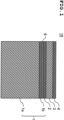
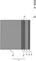
- a laminated substrate 10 of this disclosed aspect is constituted as a laminated body including a substrate 1, a lower electrode film 2 formed on the substrate 1, a piezoelectric thin film 3 formed on the lower electrode film 2, and an upper electrode film 4 formed on the piezoelectric thin film 3.
- an SOI (Silicon On Insulator) substrate a quartz glass (SiO 2 ) substrate, a gallium arsenide (GaAs) substrate, a sapphire (Al 2 O 3 ) substrate, a metal substrate made of stainless steel or the like can also be used as the substrate 1.
- the single-crystal Si-substrate 1a has a thickness of 300 to 1000 um for example, and the surface oxide film 1b has a thickness of 100 to 300 nm for example.
- the lower electrode film 2 can be formed using platinum (Pt) for example.
- the lower electrode film 2 is a single-crystal film or a poly-crystal film (they are also referred to as a Pt-film hereafter).
- crystal constituting the Pt-film is oriented preferentially in (111) plane direction with respect to a surface of the substrate 1.
- a surface of the Pt-film (a surface which is a base of the piezoelectric thin film 3) is mainly constituted of Pt-(111) plane.
- the Pt-film can be formed using a method such as a sputtering method, or an evaporation method.
- the lower electrode film 2 may also be formed using various metals such as gold (Au), ruthenium (Ru), or iridium (Ir), an alloy mainly composed of the abovementioned various metals, or a metallic oxide such as strontium ruthenate (SrRuO 3 ) or lanthanum nickelate (LaNiO 3 ), etc.
- the adhesion layer 6 can be formed using a method such as a sputtering method, or an evaporation method.
- the lower electrode film 2 has a thickness of 100 to 300 nm for example, and the adhesion layer 6 has a thickness of 1 to 20 nm for example.
- the piezoelectric thin film 3 can be formed using alkali niobium oxide which contains potassium (K), sodium (Na), and niobium (Nb), and which is represented by a composition formula of (K 1-x Na x )NbO 3 .
- the piezoelectric thin film 3 can be formed using potassium sodium niobate (KNN).
- the piezoelectric thin film 3 is a film made of poly-crystal of KNN (also referred to as a KNN-thin film hereafter).
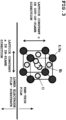
- a crystal structure of KNN is a perovskite structure as shown in FIG. 3 .
- crystal constituting the KNN-thin film is oriented preferentially in (001) plane direction with respect to the surface of the substrate 1.
- a surface of the KNN-thin film (a surface which is a base of the upper electrode film 4) is mainly constituted of KNN-(001) plane.
- 80 % or more crystal of a crystal group constituting the KNN-thin film can be oriented in (001) plane direction with respect to the surface of the substrate 1, and thereby 80 % or more region of the surface of the KNN-thin film can be KNN-(001) plane.
- the KNN-thin film can be formed using a method such as a sputtering method, a PLD (Pulsed Laser Deposition) method, or a sol-gel method.
- the piezoelectric thin film 3 has a thickness of 1 to 5 ⁇ m for example.
- the piezoelectric thin film 3 contains a metallic element selected from a group consisting of manganese (Mn) and copper (Cu) at a concentration in a range of 0.2 at% or more and 0.6 at% or less. This point will be described later.
- the upper electrode film 4 can be formed using various metals such as Pt, Au, aluminum (Al), or Cu, or an alloy of these various metals, for example.
- the upper electrode film 4 can be formed using a method such as a sputtering method, an evaporation method, a plating method, or a metal paste method.
- the upper electrode film 4 does not greatly affect the crystal structure of the piezoelectric thin film 3 unlike the lower electrode film 2. Therefore, a material and a crystal structure of the upper electrode film 4, and a method for forming the upper electrode film 4 are not particularly limited.
- An adhesion layer mainly composed of Ti, Ta, TiO 2 , Ni, etc., for example may be provided between the piezoelectric thin film 3 and the upper electrode film 4 in order to enhance an adhesion between them.
- the upper electrode film 4 has a thickness of 100 to 1000 nm for example, and the adhesion layer has a thickness of 1 to 20 nm in a case of providing the adhesion layer.
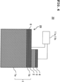
- FIG. 4 shows a schematic constitution view of a piezoelectric thin film device 30 of this disclosed aspect.
- the piezoelectric thin film device 30 is constituted including at least a piezoelectric thin film element 20 obtained by forming the abovementioned laminated substrate 10 into a prescribed shape, and a voltage detection means 11a or a voltage application means 11b connected to the piezoelectric thin film element 20.
- the piezoelectric thin film device 30 can function as a sensor.
- the piezoelectric thin film 3 is deformed according to a variation of some physical quantity, a voltage occurs between the lower electrode film 2 and the upper electrode film 4 due to the deformation.
- the piezoelectric thin film device 30 can be applied to an angular velocity sensor, an ultrasonic sensor, a pressure sensor, and an acceleration sensor, etc., for example.
- the piezoelectric thin film device 30 can function as an actuator.
- the piezoelectric thin film 3 can be deformed.
- Various members connected to the piezoelectric thin film device 30 can be actuated due to the abovementioned deformation movement.
- the piezoelectric thin film device 30 can be applied to a head for an inkjet printer, a MEMS mirror for a scanner, and a vibrator for an ultrasonic generator, etc., for example.
- the piezoelectric thin film 3 of this disclosed aspect contains the metallic element selected from the group consisting of Mn and Cu at the concentration in a range of 0.2 at% or more and 0.6 at% or less. An effect obtained thereby will be described hereafter.
- FIG. 5A explanation will be given for a processing after preparing the substrate 1 with surface oxide films 1b, 1c respectively formed on front and back surfaces of the single-crystal Si-substrate 1a, and manufacturing the laminated substrate 10 by forming the adhesion layer 6, the lower electrode film 2, and the piezoelectric thin film 3 in this order on the surface oxide film 1b on the front surface side.
- FIG. 5B there is a case that an etching is performed to the abovementioned surface electrode film 1c on the back surface side using the BHF solution, etc.
- FIG. 6A explanation will be given for a processing after preparing the substrate 1 with the surface oxide film 1b formed on a surface of a SOI substrate which is formed by laminating a single-crystal Si-substrate 1a, a BOX layer (a SiO 2 -layer) 1e, and a Si-layer 1f in this order, and manufacturing the laminated substrate 10 by forming the adhesion layer 6, the lower electrode film 2, and the piezoelectric thin film 3 in this order on the surface oxide film 1b, and then removing a part of the single-crystal Si-substrate 1a by Deep-RIE or wet etching.
- FIG. 6A explanation will be given for a processing after preparing the substrate 1 with the surface oxide film 1b formed on a surface of a SOI substrate which is formed by laminating a single-crystal Si-substrate 1a, a BOX layer (a SiO 2 -layer) 1e, and a Si-layer 1f in this order, and manufacturing
- FIG. 7A explanation will be given for a processing after forming an insulating film (a SiO 2 -film) 7 and an etching mask 7m in this order on the piezoelectric thin film 3 after patterning.
- FIG. 7B there is a case that etching is performed to a part of the insulating film 7 using the BHF solution, etc., in order to expose a region for forming the upper electrode film 4.
- the piezoelectric thin film 3 can act as etching stopper when performing the etching.
- an end-point of etching of the insulating film 7 can be controlled accurately.
- the BHF solution whose etching force is stronger than that of an etching gas such as hydrogen fluoride (HF) gas, can be used as an etchant. Therefore, an efficiency of etching can also be enhanced. Further, an etching damage of the piezoelectric thin film 3 caused by etching can be suppressed, even when performing wet etching using the BHF solution, etc.
- the concentration of Mn or Cu in the piezoelectric thin film 3 it is necessary to set the concentration of Mn or Cu in the piezoelectric thin film 3 to 0.2 at% or more and 0.6 at% or less. As described later, when the total concentration of Mn and Cu in the piezoelectric thin film 3 is less than 0.2 at%, the abovementioned effect regarding the insulation property cannot be obtained in some cases. Further, when the Cu-concentration in the piezoelectric thin film 3 is less than 0.2 at%, the abovementioned effect regarding the etching resistance cannot be obtained in some cases.
- the relative permittivity of the piezoelectric thin film 3 becomes excessive, thereby causing a deterioration of a sensitivity when the piezoelectric thin film 3 is applied to the sensor, or causing an increase of a power consumption when it is applied to the actuator, in some cases.
- One reason can be considered as follows: it is difficult to orient crystal constituting the piezoelectric thin film 3 preferentially in (001) plane direction with respect to the surface of the substrate 1, with the increase of an addition amount of Mn or Cu.
- This disclosed aspect is not limited to the abovementioned disclosed aspect, and can be modified as the following modified examples .
- the concentration of Mn or Cu in the piezoelectric thin film 3 may be set to 0.2 at% or more and 0.25 at% or less.
- the relative permittivity of the piezoelectric thin film 3 can be decreased in the abovementioned range while obtaining the abovementioned effects regarding the insulation property and the etching resistance.
- the relative permittivity of the piezoelectric thin film 3 measured under a condition of a frequency of 1 kHz, ⁇ 1 V can be in a range of 300 to 400.
- the laminated substrate 10 thus constituted can be particularly preferably applied to a high sensitive sensor, etc., which is required to have a low permittivity.
- the concentration of Mn or Cu in the piezoelectric thin film 3 may be set to 0.5 at% or more and 0.6 at% or less.
- the insulation property of the piezoelectric thin film 3 can be further enhanced while obtaining the abovementioned effects regarding the insulation property and the etching resistance.
- the leakage current density at the time of applying an electric field of 25 ⁇ 10 6 V/m to the piezoelectric thin film 3 in the thickness direction can be 500 ⁇ A/cm 2 or less.
- the laminated substrate 10 thus constituted can be particularly preferably applied to an actuator, etc., which is required to have a high withstanding pressure.
- the concentration of Cu in the piezoelectric thin film 3 may be set to 0.4 at% or more and 0.6 at% or less.
- the etching resistance of the piezoelectric thin film 3 can be further enhanced while obtaining the abovementioned effects regarding the insulation property and the relative permittivity.
- the etching rate of the piezoelectric thin film 3 can be 0.005 ⁇ m/hr or less, when the piezoelectric thin film 3 is immersed in the BHF solution having the abovementioned concentration.
- a ratio (c/a) of a lattice constant c in an out-of-plane direction with respect to a lattice constant a in an in-plane direction of crystal constituting the piezoelectric thin film 3, namely alkali niobium oxide, may be further controlled as follows, while adding Mn or Cu into the piezoelectric thin film 3 similarly to the first disclosed aspect.
- a lattice constant ratio may be controlled so that the ratio of the lattice constant c in the out-of-plane direction with respect to the lattice constant a in the in-plane direction of crystal constituting the piezoelectric thin film 3 is set in a range of 0.98 ⁇ c/a ⁇ 1.01.
- an absolute value of a piezoelectric constant of the piezoelectric thin film 3 satisfies
- the lattice constant ratio may be controlled so that the ratio of the lattice constant c in the out-of-plane direction with respect to the lattice constant a in the in-plane direction of crystal constituting at least a thickest layer of the plurality of layers is in a range of 0.98 ⁇ c/a ⁇ 1.01.
- the absolute value of the piezoelectric constant of the piezoelectric thin film 3 satisfies
- the lattice constant ratio may be controlled so that the ratio of the lattice constant c in the out-of-plane direction with respect to the lattice constant a in the in-plane direction of crystal constituting the piezoelectric thin film 3 is in a range of 0.980 ⁇ c/a ⁇ 0.993.
- the same effect as the first disclosed aspect can be obtained.
- the absolute value of the piezoelectric constant of the piezoelectric thin film 3 satisfies
- the lattice constant ratio may be controlled so that the ratio of the lattice constant c in the out-of-plane direction with respect to the lattice constant a in the in-plane direction of crystal constituting the piezoelectric thin film 3 is in a range of 1.004 ⁇ c/a ⁇ 1.010.
- the abovementioned c/a-ratio can be adjusted by controlling a partial pressure of H 2 O existing in a mixed atmosphere of argon (Ar) gas and oxygen (O 2 ) gas during sputtering film formation.
- Ar/O 2 -mixed gas is used as an atmosphere gas during sputtering film formation.
- water existing in a chamber is sometimes mixed in the atmosphere gas although its content is very small.
- the c/a-ratio of the KNN-thin film greatly depends on an orientation state in (001) plane direction of the KNN-thin film.
- the c/a-ratio tends to increase in a case of (001)-high orientation, and the c/a-ratio tends to decrease in a case of (001)-low orientation.
- This (001)-orientation state of the KNN-thin film greatly depends on the partial pressure of H 2 O contained in the atmosphere gas during sputtering film formation.
- the (001)-orientation state tends to be (001)-low orientation when H 2 O-partial pressure is high, and tends to be (001) -high orientation when H 2 O-partial pressure is low.
- the c/a-ratio of the KNN-thin film can be controlled by strictly controlling H 2 O-partial pressure in the atmosphere gas.
- a composition ratio of a substance constituting the piezoelectric thin film 3, namely alkali niobium oxide, may be controlled as follows, while adding Mn or Cu into the piezoelectric thin film 3 similarly to the first disclosed aspect.
- the piezoelectric thin film 3 may be formed using alkali niobium oxide represented by a composition formula of (K 1-x Na x ) y NbO 3 satisfying 0.4 ⁇ x ⁇ 0.7 and 0.7 ⁇ y ⁇ 0.94, and having a perovskite structure.
- the same effect as the first disclosed aspect can be obtained.
- the absolute value of the piezoelectric constant of the piezoelectric thin film 3 satisfies
- an insulation resistance of the piezoelectric thin film 3 can also be more surely improved.
- the leakage current density flowing through the piezoelectric thin film 3 at the time of applying an electric field of 50 kV/cm in the thickness direction can also be 0.1 ⁇ A/cm 2 or less.
- the piezoelectric thin film 3 may be formed using alkali niobium oxide represented by a composition formula of (K 1-x Na x ) y NbO 3 satisfying 0.4 ⁇ x ⁇ 0.7 and 0.75 ⁇ y ⁇ 0.90, and having the perovskite structure.
- the same effect as the first disclosed aspect can be obtained.
- the absolute value of the piezoelectric constant of the piezoelectric thin film 3 satisfies
- the insulation resistance of the piezoelectric thin film 3 can also be more surely improved.
- the leakage current density flowing through the piezoelectric thin film 3 at the time of applying an electric field of 50 kV/cm in the thickness direction can also be 0.1 ⁇ A/cm 2 or less.
- the abovementioned composition ratio can be adjusted by controlling a composition of a target material used during sputtering film formation, for example.
- the target material can be manufactured by mixing and burning K 2 CO 3 -powder, Na 2 CO 3 -powder, and Nb 2 O 5 -powder, etc., for example.
- the composition of the target material can be controlled by adjusting a mixed ratio of K 2 CO 3 -powder, Na 2 CO 3 -powder, and Nb 2 O 5 -powder, etc.
- composition ratio of the substance constituting the piezoelectric thin film 3 and the c/a-ratio of the lattice constant c in the out-of-plane direction with respect to the lattice constant a in the in-plane direction may be further controlled respectively as follows, while adding Mn or Cu into the piezoelectric thin film 3 similarly to the first disclosed aspect.
- the piezoelectric thin film 3 may be formed using alkali niobium oxide represented by a composition formula of (K 1-x Na x ) y NbO 3 satisfying 0.4 ⁇ x ⁇ 0.7 and 0.77 ⁇ y ⁇ 0.90, and having the perovskite structure, and the lattice constant ratio may be controlled so that the ratio of the lattice constant c in the out-of-plane direction with respect to the lattice constant a in the in-plane direction of crystal constituting the piezoelectric thin film 3 is set in a range of 0.98 ⁇ c/a ⁇ 1.008. In this case as well, the same effect as the first disclosed aspect can be obtained.
- the absolute value of the piezoelectric constant of the piezoelectric thin film 3 satisfies
- the leakage current density flowing through the piezoelectric thin film 3 at the time of applying an electric field of 50 kV/cm in the thickness direction can also be 0.1 ⁇ A/cm 2 or less.
- the lattice constant ratio may be controlled so that the ratio of the lattice constant c in the out-of-plane direction with respect to the lattice constant a in the in-plane direction of crystal constituting at least a thickest layer of the plurality of layers is set in a range of 0.98 ⁇ c/a ⁇ 1.008.
- the absolute value of the piezoelectric constant of the piezoelectric thin film 3 satisfies
- the abovementioned c/a-ratio and the composition ratio can be controlled by the method described in the second disclosed aspect and the third disclosed aspect.
- a concentration of carbon (C) or hydrogen (H) in the piezoelectric thin film 3 may be further controlled respectively as follows, while adding Mn or Cu into the piezoelectric thin film 3 similarly to the first disclosed aspect.
- a C-concentration in the piezoelectric thin film 3 may be set to 2 ⁇ 10 19 cm -3 or less, or a H-concentration therein may be set to 4 ⁇ 10 19 cm -3 or less, when being measured using SIMS.
- the insulation resistance of the piezoelectric thin film 3 can also be more surely improved.
- the leakage current density flowing through the piezoelectric thin film 3 at the time of applying an electric field of 50 kV/cm in the thickness direction can also be 0.1 ⁇ A/cm 2 or less.
- a dielectric loss tan ⁇ of the piezoelectric thin film 3 can also be 0.1 or less.
- the C-concentration in the piezoelectric thin film 3 may be set to 2 ⁇ 10 19 cm -3 or less, and the H-concentration therein may be set to 4 ⁇ 10 19 cm -3 or less.
- the insulation resistance of the piezoelectric thin film 3 can also be more surely improved.
- the leakage current density flowing through the piezoelectric thin film 3 at the time of applying an electric field of 50 kV/cm in the thickness direction can be 0.1 ⁇ A/cm 2 or less.
- the dielectric loss tan ⁇ of the piezoelectric thin film 3 can also be 0.1 or less.
- the C-concentration and the H-concentration in the sintered compact target can be more decreased when setting a burning temperature higher for manufacturing the sintered compact target. Further, it is also effective to increase a ratio of O 2 in an atmosphere gas, for example in a mixed gas of Ar-gas and O 2 -gas, when performing sputtering film formation. Further, it is also effective to perform a heat-treatment in an atmospheric air or an oxygen atmosphere after forming the piezoelectric thin film 3.
- a Si-substrate 1a with an insulating film 1d formed on its surface may be used as the substrate 1, the insulating film 1d being made of an insulating material other than SiO 2 .
- the adhesion layer 6, the lower electrode film 2, the piezoelectric thin film 3, and the upper electrode film 4 are formed in this order on the insulating film 1d, the same effect as the abovementioned each disclosed aspect, etc., can be obtained by controlling a composition or an crystal orientation of the piezoelectric thin film 3 similarly to the abovementioned each disclosed aspect.
- the adhesion layer may be provided between the piezoelectric thin film 3 and the upper electrode film 4. This point is same as the first disclosed aspect.
- a laminated substrate was manufactured by forming a Ti-layer (thickness of 2 nm) as an adhesion layer, a Pt-film (oriented preferentially in (111) plane direction with respect to a surface of the substrate and having a thickness of 200 nm) as a lower electrode film, and a KNN-thin film (oriented preferentially in (001) plane direction with respect to the surface of the substrate and having a thickness of 2 um) as a piezoelectric thin film in this order on the thermal oxide film of the substrate.
- a Cu-concentration (CuO-concentration) in the KNN-thin film was varied in a range of 0 to 1 at%.
- All of the Ti-layer, the Pt-film, and the KNN-thin film were formed by an RF magnetron sputtering method.
- a processing condition for forming the Ti-layer and the Pt-film was set as a substrate temperature: 300 °C, a discharge power: 1200 W, a charging gas: Ar, a pressure in Ar atmosphere: 0.3 Pa, and a film formation time: 5 minutes, respectively.
- the target material was formed as follows : K 2 CO 3 -powder, Na 2 CO 3 -powder, Nb 2 O 5 -powder, and CuO-powder were mixed for 24 hours using a ball mill, the mixture was provisionally burned at 850 °C for 10 hours, then pulverized using again the ball mill, and molded under a pressure of 200 MPa, and thereafter burned at 1080 °C.
- the composition of the target material was controlled by adjusting a mixed ratio of K 2 CO 3 -powder, Na 2 CO 3 -powder, Nb 2 O 5 -powder, and CuO-powder, and measured by EDX (energy dispersive X-ray spectrometry) before film formation is performed.
- FIG. 8A is a view showing an evaluation result regarding the etching resistance of the KNN-thin film
- FIG. 8B is a view showing an evaluation result regarding the insulation property of the KNN-thin film
- FIG. 8C is a view showing an evaluation result regarding the relative permittivity of the KNN-thin film.
- the evaluation of the etching-resistant was performed as follows: the laminated substrate was immersed in a BHF solution in a state that a surface of the KNN-thin film is exposed, and a time from the immersion to start of surface erosion of the KNN-thin film was measured. A HF-concentration in the BHF solution was set to 4.32 mol/L, and a NH 4 F-concentration therein was set to 10.67 mol/L.
- the etching resistance of the KNN-thin film could be dramatically enhanced by setting the Cu-concentration in the KNN-thin film to 0.2 at% or more, and the etching resistance of the KNN-thin film could be further enhanced by setting the Cu-concentration in the film to 0.5 at% or more. Further, it was confirmed that the abovementioned effect regarding the etching resistance could be hardly obtained, when Mn instead of Cu was added into the KNN-thin film.
- the evaluation of the insulation property was performed as follows: a circular Pt-film with a diameter of 0.5 mm was formed on the KNN-thin film as an upper electrode film so that a voltage could be applied between the lower electrode film and the upper electrode film, and a voltage value was measured up to a leakage current of 500 ⁇ A/cm 2 flowing between these films.
- the insulation property of the KNN-thin film could be dramatically enhanced by setting the Cu-concentration in the KNN-thin film to 0.2 at% or more, and the insulation property of the KNN-thin film could be further enhanced by setting the Cu-concentration in this film to 0.25 at% or more, further 0.5 at% or more. Further, it was confirmed that the abovementioned effect regarding the insulation property could be obtained similarly to a case of adding Cu into the KNN-thin film, even when adding Mn instead of Cu into the KNN-thin film. In this case, a preferred concentration range of a Mn-concentration was the same as the abovementioned Cu-concentration range.
- the evaluation of the relative permittivity was performed by measuring it by applying an alternating electric field of 1 kHz and ⁇ 1 V to the KNN-thin film.
- the KNN-thin film in which the Cu-concentration was set to 0.7 at% or more had the relative permittivity exceeding 1000. Further, it was confirmed that the KNN-thin film in which the Cu-concentration was set to 0.6 at% or less had the relative permittivity of less than 1000. Further, it was confirmed that the KNN-thin film in which the Cu-concentration was set to 0.25 at% or less had the relative permittivity of less than 400.
- the KNN-thin film had the relative permittivity suitable for applying to a sensor and an actuator by setting the Cu-concentration in the KNN-thin film to 0.6 at% or less, and the KNN-thin film had the relative permittivity suitable for applying to a high sensitivity sensor by setting the Cu-concentration in the film to 0.25 at% or less. Further, it was confirmed that the abovementioned effect regarding the relative permittivity could be obtained similarly to a case of adding Cu into the KNN-thin film, even when adding Mn instead of Cu into the KNN-thin film. In this case, the preferred concentration range of the Mn-concentration was the same as the abovementioned Cu-concentration range.
- a sputtering target material which is made of a sintered compact represented by a composition formula of (K 1-x Na x )NbO 3 with 0 ⁇ x ⁇ 1 and which contains at a concentration of 0.2 at% or more and 0.6 at% or less.
- a concentration of Cu in the sintered compact is 0.2 at% or more and 0.25 at% or less.
- a concentration of Cu in the sintered compact is 0.5 at% or more and 0.6 at% or less.
- a concentration of Cu in the sintered compact is 0.4 at% or more and 0.6 at% or less.
Landscapes
- Chemical & Material Sciences (AREA)
- Engineering & Computer Science (AREA)
- Organic Chemistry (AREA)
- Materials Engineering (AREA)
- Chemical Kinetics & Catalysis (AREA)
- Mechanical Engineering (AREA)
- Metallurgy (AREA)
- Acoustics & Sound (AREA)
- Physics & Mathematics (AREA)
- Ceramic Engineering (AREA)
- Inorganic Chemistry (AREA)
- Manufacturing & Machinery (AREA)
- Dispersion Chemistry (AREA)
- Particle Formation And Scattering Control In Inkjet Printers (AREA)
- Physical Vapour Deposition (AREA)
- Inorganic Compounds Of Heavy Metals (AREA)
Applications Claiming Priority (3)
| Application Number | Priority Date | Filing Date | Title |
|---|---|---|---|
| JP2015204179A JP6239566B2 (ja) | 2015-10-16 | 2015-10-16 | 圧電薄膜付き積層基板、圧電薄膜素子およびその製造方法 |
| EP16855387.3A EP3364471B1 (en) | 2015-10-16 | 2016-10-11 | Multilayer substrate with piezoelectric thin film, piezoelectric thin film element and method for manufacturing same |
| PCT/JP2016/080105 WO2017065133A1 (ja) | 2015-10-16 | 2016-10-11 | 圧電薄膜付き積層基板、圧電薄膜素子およびその製造方法 |
Related Parent Applications (1)
| Application Number | Title | Priority Date | Filing Date |
|---|---|---|---|
| EP16855387.3A Division EP3364471B1 (en) | 2015-10-16 | 2016-10-11 | Multilayer substrate with piezoelectric thin film, piezoelectric thin film element and method for manufacturing same |
Publications (3)
| Publication Number | Publication Date |
|---|---|
| EP3922749A1 EP3922749A1 (en) | 2021-12-15 |
| EP3922749B1 true EP3922749B1 (en) | 2024-12-04 |
| EP3922749C0 EP3922749C0 (en) | 2024-12-04 |
Family
ID=58517183
Family Applications (2)
| Application Number | Title | Priority Date | Filing Date |
|---|---|---|---|
| EP16855387.3A Active EP3364471B1 (en) | 2015-10-16 | 2016-10-11 | Multilayer substrate with piezoelectric thin film, piezoelectric thin film element and method for manufacturing same |
| EP21184166.3A Active EP3922749B1 (en) | 2015-10-16 | 2016-10-11 | Sputtering target for manufacturing piezoelectric thin films and method of manufacturing the sputtering target |
Family Applications Before (1)
| Application Number | Title | Priority Date | Filing Date |
|---|---|---|---|
| EP16855387.3A Active EP3364471B1 (en) | 2015-10-16 | 2016-10-11 | Multilayer substrate with piezoelectric thin film, piezoelectric thin film element and method for manufacturing same |
Country Status (4)
| Country | Link |
|---|---|
| US (2) | US11107971B2 (enExample) |
| EP (2) | EP3364471B1 (enExample) |
| JP (1) | JP6239566B2 (enExample) |
| WO (1) | WO2017065133A1 (enExample) |
Families Citing this family (19)
| Publication number | Priority date | Publication date | Assignee | Title |
|---|---|---|---|---|
| US11239410B2 (en) | 2017-03-28 | 2022-02-01 | Tdk Corporation | Piezoelectric composition and piezoelectric element |
| JP6872966B2 (ja) * | 2017-05-10 | 2021-05-19 | 住友化学株式会社 | 圧電膜を有する積層基板、圧電膜を有するデバイスおよび圧電膜を有するデバイスの製造方法 |
| JP6904101B2 (ja) * | 2017-06-26 | 2021-07-14 | セイコーエプソン株式会社 | 液体噴射ヘッド、液体噴射装置および圧電デバイス |
| JP2019021994A (ja) * | 2017-07-12 | 2019-02-07 | 株式会社サイオクス | 圧電膜を有する積層基板、圧電膜を有する素子および圧電膜を有する積層基板の製造方法 |
| JP7320098B2 (ja) * | 2018-03-14 | 2023-08-02 | 住友化学株式会社 | 圧電積層体、圧電積層体の製造方法および圧電デバイス |
| JP7074512B2 (ja) * | 2018-03-14 | 2022-05-24 | 住友化学株式会社 | 圧電積層体、圧電積層体の製造方法、圧電素子、およびスパッタリングターゲット材 |
| JP7044600B2 (ja) | 2018-03-14 | 2022-03-30 | 住友化学株式会社 | 圧電積層体、圧電積層体の製造方法および圧電デバイス |
| JP7352347B2 (ja) * | 2018-12-07 | 2023-09-28 | 住友化学株式会社 | 圧電積層体、圧電素子および圧電積層体の製造方法 |
| JP6756886B1 (ja) * | 2019-04-26 | 2020-09-16 | Jx金属株式会社 | ニオブ酸カリウムナトリウムスパッタリングターゲット |
| JP7464360B2 (ja) * | 2019-07-04 | 2024-04-09 | 住友化学株式会社 | 圧電積層体、圧電素子および圧電積層体の製造方法 |
| JP7701778B2 (ja) * | 2019-08-02 | 2025-07-02 | 住友化学株式会社 | 圧電積層体、および圧電素子 |
| JP7626383B2 (ja) * | 2019-08-02 | 2025-02-07 | 住友化学株式会社 | 圧電積層体、圧電素子および圧電積層体の製造方法 |
| JP7362339B2 (ja) * | 2019-08-02 | 2023-10-17 | 住友化学株式会社 | 圧電積層体、圧電素子、および圧電積層体の製造方法 |
| JP7679976B2 (ja) * | 2020-04-24 | 2025-05-20 | ナショナル ユニヴァーシティー オブ シンガポール | 圧電薄膜及びその作製方法 |
| EP4174024A4 (en) * | 2020-06-30 | 2024-10-09 | Sumitomo Chemical Company, Limited | Piezoelectric laminate, piezoelectric element, and method for manufacturing piezoelectric laminate |
| JP7320091B2 (ja) * | 2021-02-10 | 2023-08-02 | 住友化学株式会社 | 圧電薄膜付き積層基板、圧電薄膜付き積層基板の製造方法、圧電薄膜素子、スパッタリングターゲット材、およびスパッタリングターゲット材の製造方法 |
| JP7733503B2 (ja) | 2021-08-23 | 2025-09-03 | 住友化学株式会社 | 圧電積層体、圧電積層体の製造方法、スパッタリングターゲット材、及びスパッタリングターゲット材の製造方法 |
| JP2024141260A (ja) | 2023-03-29 | 2024-10-10 | 住友化学株式会社 | 圧電積層体、圧電積層体の製造方法、及び圧電素子 |
| JP2024141259A (ja) * | 2023-03-29 | 2024-10-10 | 住友化学株式会社 | 圧電積層体、圧電積層体の製造方法、及び圧電素子 |
Citations (1)
| Publication number | Priority date | Publication date | Assignee | Title |
|---|---|---|---|---|
| US20040127344A1 (en) * | 2002-09-24 | 2004-07-01 | Noritake Co., Limited | Lead-free piezoelectric ceramic composition wherein Cu is contained in (KxA1-x)y(Nb1-zBz)O3 perovskite compound, and process of preparing the same |
Family Cites Families (26)
| Publication number | Priority date | Publication date | Assignee | Title |
|---|---|---|---|---|
| EP0294142B1 (en) * | 1987-06-01 | 1992-03-25 | Japan Pionics., Ltd. | Method of cleaning exhaust gases |
| JP3531803B2 (ja) | 1999-02-24 | 2004-05-31 | 株式会社豊田中央研究所 | アルカリ金属含有ニオブ酸化物系圧電材料組成物 |
| US6692652B2 (en) | 2001-04-23 | 2004-02-17 | Kabushiki Kaisha Toyota Chuo Kenkyusho | Grain oriented ceramics |
| US6903491B2 (en) * | 2001-04-26 | 2005-06-07 | Matsushita Electric Industrial Co., Ltd. | Piezoelectric element, actuator, and inkjet head |
| JP4735840B2 (ja) | 2005-12-06 | 2011-07-27 | セイコーエプソン株式会社 | 圧電体積層体、表面弾性波素子、薄膜圧電共振子および圧電アクチュエータ |
| EP2009148A4 (en) * | 2006-03-20 | 2011-05-25 | Kanagawa Kagaku Gijutsu Akad | GROUP III-V NITRIDE LAYER AND MANUFACTURING METHOD THEREFOR |
| JP2008159807A (ja) | 2006-12-22 | 2008-07-10 | Hitachi Cable Ltd | 圧電薄膜素子及び圧電薄膜素子を用いて製造したアクチュエータとセンサ |
| JP5181538B2 (ja) | 2007-06-06 | 2013-04-10 | 日立電線株式会社 | 圧電体及び圧電素子 |
| JP5525143B2 (ja) * | 2008-06-05 | 2014-06-18 | 日立金属株式会社 | 圧電薄膜素子及び圧電薄膜デバイス |
| JP5314963B2 (ja) * | 2008-08-12 | 2013-10-16 | 富士フイルム株式会社 | 積層体、圧電素子、および液体吐出装置 |
| JP5515675B2 (ja) | 2009-11-20 | 2014-06-11 | 日立金属株式会社 | 圧電薄膜素子及び圧電薄膜デバイス |
| JP5531635B2 (ja) | 2010-01-18 | 2014-06-25 | 日立金属株式会社 | 圧電薄膜素子及び圧電薄膜デバイス |
| JP5071503B2 (ja) | 2010-03-25 | 2012-11-14 | 日立電線株式会社 | 圧電薄膜素子及び圧電薄膜デバイス |
| JP2011233817A (ja) * | 2010-04-30 | 2011-11-17 | Hitachi Cable Ltd | 圧電体素子、その製造方法、及び圧電体デバイス |
| JP5056914B2 (ja) | 2010-07-07 | 2012-10-24 | 日立電線株式会社 | 圧電薄膜素子および圧電薄膜デバイス |
| WO2012014504A1 (ja) * | 2010-07-29 | 2012-02-02 | Jx日鉱日石金属株式会社 | 磁気記録膜用スパッタリングターゲット及びその製造方法 |
| JP5380756B2 (ja) * | 2011-08-10 | 2014-01-08 | 日立金属株式会社 | 圧電体膜素子の製造方法 |
| JP2013251355A (ja) * | 2012-05-31 | 2013-12-12 | Hitachi Cable Ltd | 圧電体膜素子の製造方法、圧電体膜素子、及び圧電体デバイス |
| JP5858385B2 (ja) * | 2012-08-07 | 2016-02-10 | 住友化学株式会社 | 圧電体素子、圧電体デバイス及びその製造方法 |
| US20140084754A1 (en) * | 2012-09-21 | 2014-03-27 | Tdk Corporation | Thin film piezoelectric device |
| JP6266987B2 (ja) * | 2013-03-19 | 2018-01-24 | 住友化学株式会社 | 圧電薄膜素子、圧電センサ及び振動発電機 |
| JP2014187094A (ja) | 2013-03-22 | 2014-10-02 | Hitachi Metals Ltd | 圧電体薄膜積層基板、圧電体薄膜素子、およびそれらの製造方法 |
| US9331262B2 (en) * | 2013-05-20 | 2016-05-03 | Tdk Corporation | Thin film piezoelectric element, thin film piezoelectric actuator, thin film piezoelectric sensor, hard drive disk, and inkjet printer device |
| JP6044719B2 (ja) | 2013-09-09 | 2016-12-14 | 株式会社村田製作所 | 圧電薄膜素子及びその製造方法 |
| JP2015153850A (ja) | 2014-02-13 | 2015-08-24 | 株式会社サイオクス | 圧電体薄膜素子、その製造方法、および該圧電体薄膜素子を用いた電子デバイス |
| JP6521241B2 (ja) | 2015-05-28 | 2019-05-29 | セイコーエプソン株式会社 | 圧電素子及び圧電素子応用デバイス |
-
2015
- 2015-10-16 JP JP2015204179A patent/JP6239566B2/ja active Active
-
2016
- 2016-10-11 US US15/767,677 patent/US11107971B2/en active Active
- 2016-10-11 EP EP16855387.3A patent/EP3364471B1/en active Active
- 2016-10-11 EP EP21184166.3A patent/EP3922749B1/en active Active
- 2016-10-11 WO PCT/JP2016/080105 patent/WO2017065133A1/ja not_active Ceased
-
2021
- 2021-07-28 US US17/387,523 patent/US20210359195A1/en active Pending
Patent Citations (1)
| Publication number | Priority date | Publication date | Assignee | Title |
|---|---|---|---|---|
| US20040127344A1 (en) * | 2002-09-24 | 2004-07-01 | Noritake Co., Limited | Lead-free piezoelectric ceramic composition wherein Cu is contained in (KxA1-x)y(Nb1-zBz)O3 perovskite compound, and process of preparing the same |
Also Published As
| Publication number | Publication date |
|---|---|
| EP3922749A1 (en) | 2021-12-15 |
| EP3364471A4 (en) | 2019-10-23 |
| JP6239566B2 (ja) | 2017-11-29 |
| EP3364471A1 (en) | 2018-08-22 |
| EP3364471B1 (en) | 2021-07-14 |
| US11107971B2 (en) | 2021-08-31 |
| US20210359195A1 (en) | 2021-11-18 |
| WO2017065133A1 (ja) | 2017-04-20 |
| JP2017076730A (ja) | 2017-04-20 |
| US20180301618A1 (en) | 2018-10-18 |
| EP3922749C0 (en) | 2024-12-04 |
Similar Documents
| Publication | Publication Date | Title |
|---|---|---|
| EP3922749B1 (en) | Sputtering target for manufacturing piezoelectric thin films and method of manufacturing the sputtering target | |
| EP3772114B1 (en) | Piezoelectric element and manufacturing method thereof | |
| EP3540797B1 (en) | Piezoelectric laminate, method of manufacturing piezoelectric laminate, and piezoelectric element | |
| EP3637486B1 (en) | Laminated substrate with potassium sodium niobate piezoelectric film and manufacturing method thereof | |
| EP3540800B1 (en) | Piezoelectric laminate, method of manufacturing the piezoelectric laminate and piezoelectric device | |
| JP7022853B2 (ja) | スパッタリングターゲット材、スパッタリングターゲット材の製造方法、および圧電薄膜付き積層基板の製造方法 | |
| JP7696347B2 (ja) | 圧電積層体、圧電素子および圧電積層体の製造方法 | |
| EP3761383A1 (en) | Piezoelectric laminate, piezoelectric element and method of manufacturing the piezoelectric laminate | |
| JP6502460B2 (ja) | 圧電薄膜付き積層基板および圧電薄膜素子 | |
| JP2012253109A (ja) | 圧電膜素子及び圧電膜デバイス | |
| JP7320091B2 (ja) | 圧電薄膜付き積層基板、圧電薄膜付き積層基板の製造方法、圧電薄膜素子、スパッタリングターゲット材、およびスパッタリングターゲット材の製造方法 | |
| JP6961770B2 (ja) | 圧電薄膜付き積層基板および圧電薄膜素子 | |
| JP7399753B2 (ja) | 圧電膜、圧電積層体、圧電素子および圧電積層体の製造方法 | |
| JP6758444B2 (ja) | 圧電薄膜付き積層基板および圧電薄膜素子 | |
| EP3772115B1 (en) | Piezoelectric element and manufacturing method thereof | |
| JP7320098B2 (ja) | 圧電積層体、圧電積層体の製造方法および圧電デバイス | |
| JP6804615B2 (ja) | 圧電膜を有する積層基板、圧電膜を有する素子および圧電膜を有する積層基板の製造方法 | |
| EP3995454A1 (en) | Piezoelectric film, piezoelectric layered body, piezoelectric element, and method for manufacturing piezoelectric layered body |
Legal Events
| Date | Code | Title | Description |
|---|---|---|---|
| PUAI | Public reference made under article 153(3) epc to a published international application that has entered the european phase |
Free format text: ORIGINAL CODE: 0009012 |
|
| STAA | Information on the status of an ep patent application or granted ep patent |
Free format text: STATUS: THE APPLICATION HAS BEEN PUBLISHED |
|
| AC | Divisional application: reference to earlier application |
Ref document number: 3364471 Country of ref document: EP Kind code of ref document: P |
|
| AK | Designated contracting states |
Kind code of ref document: A1 Designated state(s): AL AT BE BG CH CY CZ DE DK EE ES FI FR GB GR HR HU IE IS IT LI LT LU LV MC MK MT NL NO PL PT RO RS SE SI SK SM TR |
|
| B565 | Issuance of search results under rule 164(2) epc |
Effective date: 20211102 |
|
| STAA | Information on the status of an ep patent application or granted ep patent |
Free format text: STATUS: REQUEST FOR EXAMINATION WAS MADE |
|
| 17P | Request for examination filed |
Effective date: 20220607 |
|
| RBV | Designated contracting states (corrected) |
Designated state(s): AL AT BE BG CH CY CZ DE DK EE ES FI FR GB GR HR HU IE IS IT LI LT LU LV MC MK MT NL NO PL PT RO RS SE SI SK SM TR |
|
| GRAP | Despatch of communication of intention to grant a patent |
Free format text: ORIGINAL CODE: EPIDOSNIGR1 |
|
| STAA | Information on the status of an ep patent application or granted ep patent |
Free format text: STATUS: GRANT OF PATENT IS INTENDED |
|
| RIC1 | Information provided on ipc code assigned before grant |
Ipc: H10N 30/853 20230101ALI20240513BHEP Ipc: H10N 30/076 20230101ALI20240513BHEP Ipc: C23C 14/08 20060101ALI20240513BHEP Ipc: C23C 14/34 20060101AFI20240513BHEP |
|
| INTG | Intention to grant announced |
Effective date: 20240607 |
|
| RIN1 | Information on inventor provided before grant (corrected) |
Inventor name: HORIKIRI, FUMIMASA Inventor name: WATANABE, KAZUTOSHI Inventor name: SHIBATA, KENJI |
|
| GRAS | Grant fee paid |
Free format text: ORIGINAL CODE: EPIDOSNIGR3 |
|
| GRAA | (expected) grant |
Free format text: ORIGINAL CODE: 0009210 |
|
| STAA | Information on the status of an ep patent application or granted ep patent |
Free format text: STATUS: THE PATENT HAS BEEN GRANTED |
|
| RAP3 | Party data changed (applicant data changed or rights of an application transferred) |
Owner name: SUMITOMO CHEMICAL COMPANY, LIMITED |
|
| AC | Divisional application: reference to earlier application |
Ref document number: 3364471 Country of ref document: EP Kind code of ref document: P |
|
| AK | Designated contracting states |
Kind code of ref document: B1 Designated state(s): AL AT BE BG CH CY CZ DE DK EE ES FI FR GB GR HR HU IE IS IT LI LT LU LV MC MK MT NL NO PL PT RO RS SE SI SK SM TR |
|
| REG | Reference to a national code |
Ref country code: CH Ref legal event code: EP |
|
| REG | Reference to a national code |
Ref country code: DE Ref legal event code: R096 Ref document number: 602016090558 Country of ref document: DE |
|
| REG | Reference to a national code |
Ref country code: IE Ref legal event code: FG4D |
|
| U01 | Request for unitary effect filed |
Effective date: 20241204 |
|
| U07 | Unitary effect registered |
Designated state(s): AT BE BG DE DK EE FI FR IT LT LU LV MT NL PT RO SE SI Effective date: 20241212 |
|
| PG25 | Lapsed in a contracting state [announced via postgrant information from national office to epo] |
Ref country code: HR Free format text: LAPSE BECAUSE OF FAILURE TO SUBMIT A TRANSLATION OF THE DESCRIPTION OR TO PAY THE FEE WITHIN THE PRESCRIBED TIME-LIMIT Effective date: 20241204 |
|
| PG25 | Lapsed in a contracting state [announced via postgrant information from national office to epo] |
Ref country code: ES Free format text: LAPSE BECAUSE OF FAILURE TO SUBMIT A TRANSLATION OF THE DESCRIPTION OR TO PAY THE FEE WITHIN THE PRESCRIBED TIME-LIMIT Effective date: 20241204 |
|
| PG25 | Lapsed in a contracting state [announced via postgrant information from national office to epo] |
Ref country code: NO Free format text: LAPSE BECAUSE OF FAILURE TO SUBMIT A TRANSLATION OF THE DESCRIPTION OR TO PAY THE FEE WITHIN THE PRESCRIBED TIME-LIMIT Effective date: 20250304 |
|
| PG25 | Lapsed in a contracting state [announced via postgrant information from national office to epo] |
Ref country code: GR Free format text: LAPSE BECAUSE OF FAILURE TO SUBMIT A TRANSLATION OF THE DESCRIPTION OR TO PAY THE FEE WITHIN THE PRESCRIBED TIME-LIMIT Effective date: 20250305 |
|
| PG25 | Lapsed in a contracting state [announced via postgrant information from national office to epo] |
Ref country code: RS Free format text: LAPSE BECAUSE OF FAILURE TO SUBMIT A TRANSLATION OF THE DESCRIPTION OR TO PAY THE FEE WITHIN THE PRESCRIBED TIME-LIMIT Effective date: 20250304 |
|
| PG25 | Lapsed in a contracting state [announced via postgrant information from national office to epo] |
Ref country code: SM Free format text: LAPSE BECAUSE OF FAILURE TO SUBMIT A TRANSLATION OF THE DESCRIPTION OR TO PAY THE FEE WITHIN THE PRESCRIBED TIME-LIMIT Effective date: 20241204 |
|
| PG25 | Lapsed in a contracting state [announced via postgrant information from national office to epo] |
Ref country code: PL Free format text: LAPSE BECAUSE OF FAILURE TO SUBMIT A TRANSLATION OF THE DESCRIPTION OR TO PAY THE FEE WITHIN THE PRESCRIBED TIME-LIMIT Effective date: 20241204 |
|
| PG25 | Lapsed in a contracting state [announced via postgrant information from national office to epo] |
Ref country code: IS Free format text: LAPSE BECAUSE OF FAILURE TO SUBMIT A TRANSLATION OF THE DESCRIPTION OR TO PAY THE FEE WITHIN THE PRESCRIBED TIME-LIMIT Effective date: 20250404 |
|
| PG25 | Lapsed in a contracting state [announced via postgrant information from national office to epo] |
Ref country code: SK Free format text: LAPSE BECAUSE OF FAILURE TO SUBMIT A TRANSLATION OF THE DESCRIPTION OR TO PAY THE FEE WITHIN THE PRESCRIBED TIME-LIMIT Effective date: 20241204 |
|
| PG25 | Lapsed in a contracting state [announced via postgrant information from national office to epo] |
Ref country code: CZ Free format text: LAPSE BECAUSE OF FAILURE TO SUBMIT A TRANSLATION OF THE DESCRIPTION OR TO PAY THE FEE WITHIN THE PRESCRIBED TIME-LIMIT Effective date: 20241204 |
|
| PLBE | No opposition filed within time limit |
Free format text: ORIGINAL CODE: 0009261 |
|
| STAA | Information on the status of an ep patent application or granted ep patent |
Free format text: STATUS: NO OPPOSITION FILED WITHIN TIME LIMIT |
|
| U20 | Renewal fee for the european patent with unitary effect paid |
Year of fee payment: 10 Effective date: 20250923 |
|
| 26N | No opposition filed |
Effective date: 20250905 |