EP3910667A1 - Packaging glass substrate for semiconductor, packaging substrate for semiconductor, and semiconductor device - Google Patents
Packaging glass substrate for semiconductor, packaging substrate for semiconductor, and semiconductor device Download PDFInfo
- Publication number
- EP3910667A1 EP3910667A1 EP20783657.8A EP20783657A EP3910667A1 EP 3910667 A1 EP3910667 A1 EP 3910667A1 EP 20783657 A EP20783657 A EP 20783657A EP 3910667 A1 EP3910667 A1 EP 3910667A1
- Authority
- EP
- European Patent Office
- Prior art keywords
- glass substrate
- semiconductor
- layer
- core
- packaging
- Prior art date
- Legal status (The legal status is an assumption and is not a legal conclusion. Google has not performed a legal analysis and makes no representation as to the accuracy of the status listed.)
- Granted
Links
Images




Classifications
-
- H—ELECTRICITY
- H10—SEMICONDUCTOR DEVICES; ELECTRIC SOLID-STATE DEVICES NOT OTHERWISE PROVIDED FOR
- H10W—GENERIC PACKAGES, INTERCONNECTIONS, CONNECTORS OR OTHER CONSTRUCTIONAL DETAILS OF DEVICES COVERED BY CLASS H10
- H10W70/00—Package substrates; Interposers; Redistribution layers [RDL]
- H10W70/60—Insulating or insulated package substrates; Interposers; Redistribution layers
- H10W70/62—Insulating or insulated package substrates; Interposers; Redistribution layers characterised by their interconnections
- H10W70/63—Vias, e.g. via plugs
- H10W70/635—Through-vias
-
- H—ELECTRICITY
- H10—SEMICONDUCTOR DEVICES; ELECTRIC SOLID-STATE DEVICES NOT OTHERWISE PROVIDED FOR
- H10W—GENERIC PACKAGES, INTERCONNECTIONS, CONNECTORS OR OTHER CONSTRUCTIONAL DETAILS OF DEVICES COVERED BY CLASS H10
- H10W70/00—Package substrates; Interposers; Redistribution layers [RDL]
- H10W70/01—Manufacture or treatment
- H10W70/05—Manufacture or treatment of insulating or insulated package substrates, or of interposers, or of redistribution layers
-
- H—ELECTRICITY
- H10—SEMICONDUCTOR DEVICES; ELECTRIC SOLID-STATE DEVICES NOT OTHERWISE PROVIDED FOR
- H10W—GENERIC PACKAGES, INTERCONNECTIONS, CONNECTORS OR OTHER CONSTRUCTIONAL DETAILS OF DEVICES COVERED BY CLASS H10
- H10W70/00—Package substrates; Interposers; Redistribution layers [RDL]
- H10W70/01—Manufacture or treatment
- H10W70/05—Manufacture or treatment of insulating or insulated package substrates, or of interposers, or of redistribution layers
- H10W70/095—Manufacture or treatment of insulating or insulated package substrates, or of interposers, or of redistribution layers of vias therein
-
- H—ELECTRICITY
- H10—SEMICONDUCTOR DEVICES; ELECTRIC SOLID-STATE DEVICES NOT OTHERWISE PROVIDED FOR
- H10W—GENERIC PACKAGES, INTERCONNECTIONS, CONNECTORS OR OTHER CONSTRUCTIONAL DETAILS OF DEVICES COVERED BY CLASS H10
- H10W70/00—Package substrates; Interposers; Redistribution layers [RDL]
- H10W70/60—Insulating or insulated package substrates; Interposers; Redistribution layers
- H10W70/62—Insulating or insulated package substrates; Interposers; Redistribution layers characterised by their interconnections
- H10W70/65—Shapes or dispositions of interconnections
-
- H—ELECTRICITY
- H10—SEMICONDUCTOR DEVICES; ELECTRIC SOLID-STATE DEVICES NOT OTHERWISE PROVIDED FOR
- H10W—GENERIC PACKAGES, INTERCONNECTIONS, CONNECTORS OR OTHER CONSTRUCTIONAL DETAILS OF DEVICES COVERED BY CLASS H10
- H10W70/00—Package substrates; Interposers; Redistribution layers [RDL]
- H10W70/60—Insulating or insulated package substrates; Interposers; Redistribution layers
- H10W70/67—Insulating or insulated package substrates; Interposers; Redistribution layers characterised by their insulating layers or insulating parts
- H10W70/68—Shapes or dispositions thereof
-
- H—ELECTRICITY
- H10—SEMICONDUCTOR DEVICES; ELECTRIC SOLID-STATE DEVICES NOT OTHERWISE PROVIDED FOR
- H10W—GENERIC PACKAGES, INTERCONNECTIONS, CONNECTORS OR OTHER CONSTRUCTIONAL DETAILS OF DEVICES COVERED BY CLASS H10
- H10W70/00—Package substrates; Interposers; Redistribution layers [RDL]
- H10W70/60—Insulating or insulated package substrates; Interposers; Redistribution layers
- H10W70/67—Insulating or insulated package substrates; Interposers; Redistribution layers characterised by their insulating layers or insulating parts
- H10W70/69—Insulating materials thereof
- H10W70/692—Ceramics or glasses
-
- H—ELECTRICITY
- H10—SEMICONDUCTOR DEVICES; ELECTRIC SOLID-STATE DEVICES NOT OTHERWISE PROVIDED FOR
- H10W—GENERIC PACKAGES, INTERCONNECTIONS, CONNECTORS OR OTHER CONSTRUCTIONAL DETAILS OF DEVICES COVERED BY CLASS H10
- H10W72/00—Interconnections or connectors in packages
-
- H—ELECTRICITY
- H10—SEMICONDUCTOR DEVICES; ELECTRIC SOLID-STATE DEVICES NOT OTHERWISE PROVIDED FOR
- H10W—GENERIC PACKAGES, INTERCONNECTIONS, CONNECTORS OR OTHER CONSTRUCTIONAL DETAILS OF DEVICES COVERED BY CLASS H10
- H10W90/00—Package configurations
- H10W90/401—Package configurations characterised by multiple insulating or insulated package substrates, interposers or RDLs
-
- H—ELECTRICITY
- H10—SEMICONDUCTOR DEVICES; ELECTRIC SOLID-STATE DEVICES NOT OTHERWISE PROVIDED FOR
- H10W—GENERIC PACKAGES, INTERCONNECTIONS, CONNECTORS OR OTHER CONSTRUCTIONAL DETAILS OF DEVICES COVERED BY CLASS H10
- H10W90/00—Package configurations
-
- H—ELECTRICITY
- H10—SEMICONDUCTOR DEVICES; ELECTRIC SOLID-STATE DEVICES NOT OTHERWISE PROVIDED FOR
- H10W—GENERIC PACKAGES, INTERCONNECTIONS, CONNECTORS OR OTHER CONSTRUCTIONAL DETAILS OF DEVICES COVERED BY CLASS H10
- H10W90/00—Package configurations
- H10W90/701—Package configurations characterised by the relative positions of pads or connectors relative to package parts
-
- H—ELECTRICITY
- H10—SEMICONDUCTOR DEVICES; ELECTRIC SOLID-STATE DEVICES NOT OTHERWISE PROVIDED FOR
- H10W—GENERIC PACKAGES, INTERCONNECTIONS, CONNECTORS OR OTHER CONSTRUCTIONAL DETAILS OF DEVICES COVERED BY CLASS H10
- H10W90/00—Package configurations
- H10W90/701—Package configurations characterised by the relative positions of pads or connectors relative to package parts
- H10W90/721—Package configurations characterised by the relative positions of pads or connectors relative to package parts of bump connectors
- H10W90/722—Package configurations characterised by the relative positions of pads or connectors relative to package parts of bump connectors between stacked chips
-
- H—ELECTRICITY
- H10—SEMICONDUCTOR DEVICES; ELECTRIC SOLID-STATE DEVICES NOT OTHERWISE PROVIDED FOR
- H10W—GENERIC PACKAGES, INTERCONNECTIONS, CONNECTORS OR OTHER CONSTRUCTIONAL DETAILS OF DEVICES COVERED BY CLASS H10
- H10W90/00—Package configurations
- H10W90/701—Package configurations characterised by the relative positions of pads or connectors relative to package parts
- H10W90/721—Package configurations characterised by the relative positions of pads or connectors relative to package parts of bump connectors
- H10W90/724—Package configurations characterised by the relative positions of pads or connectors relative to package parts of bump connectors between a chip and a stacked insulating package substrate, interposer or RDL
Definitions
- the embodiments relate to a packaging glass substrate for semiconductor, a packaging substrate for semiconductor, and a semiconductor apparatus.
- FE Front-End Process
- BE Back-End Process
- a packaging process is included in the Back-End process.
- semiconductor technology has been developed in various forms such as line width of a nanometer unit, which is smaller than a micrometer unit, 10 million or more cells, high-speed operation, and much heat dissipation, but technology of packaging it completely is not supported yet.
- the electrical performance of semiconductors may be determined by the packaging technology and the resulting electrical connection rather than the performance of the semiconductor itself.
- Ceramic or resin is used as the material of a packaging substrate.
- a ceramic substrate such as Si substrate, it is not easy to mount a high-performance and high-frequency semiconductor element thereon due to a high resistance or high dielectric constant.
- the objective of the present disclosure is to provide a packaging glass substrate for semiconductor, a packaging substrate for semiconductor, a semiconductor apparatus, and the like, which can be used to manufacture a more integrated semiconductor apparatus by applying a glass substrate of which stress is controlled and a semiconductor apparatus packaging substrate including the same, and the like.
- a packaging glass substrate for semiconductor includes a glass substrate with a first surface and a second surface facing each other; and a plurality of core via penetrating through the glass substrate in a thickness direction.
- a plain line is a line linking places where the core via is not formed.
- a via line is a line linking places where the core via is formed.
- a stress difference value (P) is a value according to the below Equation (1).
- P Vp ⁇ Np
- the P is a stress difference value measured at the same glass substrate
- the Vp is a difference between the maximum value and the minimum value of stress measured at the via line
- the Np is a difference between the maximum value and the minimum value of stress measured at the plain line.
- a stress difference value (P) of a packaging glass substrate for semiconductor is 1.5 MPa or less.
- the Vp value may be 2.5 MPa or less.
- the Np value may be 1.0 MPa or less.
- the core via may be disposed in the number of 100 to 3000, based on a unit area (1cm x 1cm) of the glass substrate.
- a stress difference ratio (K) is a value according to the below Equation (2).
- K Lp / La
- the K is a stress difference ratio measured at the same plane of the same glass substrate
- the Lp is a difference between the maximum value and the minimum value of stress measured at a target line
- the La is an average value of stress measured at the target line.
- a glass substrate for packaging according to one embodiment may have a stress difference ratio (K) of 6 or less.
- the target line may be a plain line, and a stress difference ratio (K) of the glass substrate for semiconductor packaging may be 2 or less.
- the target line may be a via line, and a stress difference ratio (K) of the glass substrate for semiconductor packaging may be 6 or less.
- the core via may be disposed in the number of 100 to 3000, based on a unit area (1cm x 1cm) of the glass substrate.
- a packaging substrate for semiconductor includes a packaging glass substrate for semiconductor described above, and further includes a core layer disposed on a surface of the core via, and a core seed layer to become as a seed for forming an electrically conductive layer, or a core distribution layer which is an electrically conductive layer.
- a semiconductor apparatus includes a semiconductor element unit including 1 or more semiconductor elements; a packaging substrate for semiconductor electrically connected to the semiconductor element unit; and a motherboard electrically connected to the packaging substrate, transmitting electrical signals of the semiconductor element and external, and connecting each other, wherein the packaging substrate for semiconductor is a packaging substrate for semiconductor described above.
- a glass substrate for semiconductor packaging, a substrate for semiconductor packaging, and a semiconductor apparatus of the embodiments can significantly improve electrical properties such as a signal transmission rate by connecting the semiconductor element and a motherboard to be closer to each other so that electrical signals are transmitted through as short a path as possible.
- the glass substrate applied as a core of substrate is an insulator itself, there is a lower possibility of generating parasitic element compared to a conventional silicon core, and thus it is possible to simplify the treatment process for insulating layer and it is also applicable to a high-speed circuit.
- the glass substrate is manufactured in the form of a large panel, and thus mass production is relatively easy and economic efficiency can be further improved.
- the embodiment applies a glass substrate of which stress is controlled, it may have excellent mechanical properties despite formation of core vias.
- X-based may mean that a compound includes a compound corresponding to X, or a derivative of X.
- B being disposed on A means that B is disposed in direct contact with A or disposed over A with another layer or structure interposed therebetween and thus should not be interpreted as being limited to B being disposed in direct contact with A.
- B being connected to A means that B is connected to A directly or through another element therebetween, and thus should not be interpreted as being limited to B being directly connected to A, unless otherwise noted.
- the inventors have recognized that, in the process of developing a semiconductor apparatus capable of exhibiting high performance with a more integrated and thinner thickness, not only the apparatus itself but also the packaging process is an important factor for improving its performance. Also, inventors have confirmed that, by applying a glass core in a single layer and controlling the shape of a through-via, an electrically conductive layer formed thereon, etc., it is possible to make a packaging substrate thinner and to improve the electrical properties of the semiconductor apparatus, unlike a conventional interposer and organic substrate in which two or more layers of cores are applied on a motherboard as a packaging substrate.
- a substrate for packaging applied with a glass substrate of which such concentration of stress is controlled is provided.
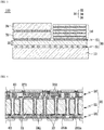
- FIG. 1 is a conceptual view for illustrating a top view (a) of a glass substrate having a core via applied in embodiments of the present disclosure and a cross section of the core via
- FIG. 2 are conceptual views for illustrating a method of measuring stress in the present disclosure, wherein (a) shows a route for measuring stress of a via line, and (b) shows a route for measuring stress of a plain line.
- FIG. 3 is a conceptual view for illustrating a cross section of a semiconductor apparatus according to one embodiment of the present disclosure
- FIG. 4 is a conceptual view for illustrating a cross section of a packaging substrate according to another embodiment of the present disclosure
- FIGs. 5 and 6 are detailed conceptual views for illustrating some of cross sections of a packaging substrate according to example embodiments of the present disclosure, respectively (a circle indicates a view obtained through observation from the top or the bottom).
- a substrate for a semiconductor packaging will be described in detail
- FIG. 3 to 6 a packaging substrate, and a semiconductor apparatus will be described in detail.
- a substrate for semiconductor packaging 215 includes a glass substrate 21, a core via 23, and a core layer 22.
- a glass substrate 21 has a first surface 213 and a second surface 214 facing each other.
- a core seed layer 225 or a core distribution pattern 241 is disposed at a core layer 22.
- a core seed layer 225 is disposed on a surface of the core via and to become as a seed for forming an electrically conductive layer.
- a core distribution pattern is an electrically conductive layer disposed on a surface of the core via.
- a glass substrate applied to semiconductor is preferable.
- a borosilicate glass substrate, a non-alkali glass substrate, or the like may be applicable, but the present disclosure is not limited thereto.
- the glass substrate 21 may have a thickness of 1,000 ⁇ m or less.
- the glass substrate 21 may have a thickness of 100 to 1,000 ⁇ m, or 100 to 700 ⁇ m.
- the glass substrate 21 may have a thickness of 100 to 500 ⁇ m.
- the glass substrate also should serve as a supporting body which supports semiconductor elements disposed thereon, so it is preferable to have the above thickness.
- the thickness of the glass substrate refers to the thickness of the glass substrate itself except for the thickness of the electrically conductive layer on the glass substrate.
- the core vias 23 may be formed by removing a predetermined region of the glass substrate 21, and in particular, it may be formed by etching a glass plate physically and/or chemically.
- Formation of the core via 23 may be applied with a method of forming a defect (flaw) on the surface of the glass substrate by means of a laser and the like and then etching chemically, laser etching, etc., but the present disclosure is not limited thereto.
- a stress of the glass substrate 21 may be measured at a plain line or a via line.
- a plain line is a line linking places where the core via 23 is not formed on a first surface 213.
- a via line is a line linking places where the core via 23 is formed on a first surface 213.
- a stress difference value (P) is represented by the below Equation (1).
- the glass substrate 21 may have a stress difference value (P) of 1.5 MPa or less.
- P Vp ⁇ Np
- the Vp is a difference between the maximum value and the minimum value of stress measured at a via line
- the Np is a difference between the maximum value and the minimum value of stress measured at a plain line.
- the P value may be 1.35 MPa or less, 1.2 MPa or less or 1.1 MPa or less. Also, the P value may be 0.01 MPa or more, or 0.1 MPa or more.
- the Vp value of the glass substrate may be 2.5 MPa or less.
- the Vp value of the glass substrate may be or 2.3 MPa or less, and the Vp value may be 2.0 MPa or less.
- the Vp value of the glass substrate may be 1.8 MPa or less.
- the Vp value of the glass substrate may be 0.2 MPa or more.
- the Vp value of the glass substrate may be 0.4 MPa or more.
- Vp glass substrate with difference
- the Np value of the glass substrate may be 1.0 MPa or less.
- the Np value of the glass substrate may be 0.9 MPa or less, or 0.8 MPa or less.
- the Np value of the glass substrate may be 0.1 MPa or more.
- the Np value of the glass substrate may be 0.2 MPa or more.
- a stress difference ratio (K) is represented by the below Equation (2).
- a target line is the one selected from a plain line which is a line linking places where a core via is not formed, or a via line which is a line linking places where a core via is formed.
- the glass substrate may have a stress difference ratio (K) of 6 or less.
- K Lp / La
- the K is a stress difference ratio measured at the same plane of the same glass substrate
- the Lp is a difference between the maximum value and the minimum value of stress measured at the target line
- the La is an average value of stress measured at the target line.
- the K value of the glass substrate may be 5 or less, 4.5 or less, or 4 or less.
- a stress difference ratio measured at a plain line is represented as Kn.
- the stress difference ratio (Kn) at a plain line may be 2 or less.
- the stress difference ratio (Kn) at a plain line may be 1.8 or less.
- the stress difference ratio (Kn) at a plain line may be more than 0.3.
- the stress difference ratio (Kn) at a plain line may be more than 0.5.
- a stress difference ratio measured at a via line is represented as Kv.
- the stress difference ratio (Kv) at a via line may be 6 or less.
- the stress difference ratio (Kv) of a via line may be 5 or less.
- the stress difference ratio (Kv) of a via line may be 4.5 or less, or 3 or less.
- the stress difference ratio (Kv) of a via line may be 0.5 or more.
- the stress difference ratio (Kv) at a via line may be 1.0 or more, or 1.5. or more.
- the stress is analyzed by applying a birefringence 2D evaluation device.
- the birefringence 2D dispersion evaluation device may be WPA-200 device of NPM(NIPPON PULSE KOREA CO., LTD).
- measured values such as a birefringence value are inputted by the device, and stress in a measuring route is presented by pressure unit (ex. MPa) through a predetermined calculation process.
- stress can be measured by inputting a light elastic coefficient and the thickness of a measuring target, and 2.4 is applied as the light elastic value in the examples.
- the core via 23 may be disposed in the number of 100 to 3000, or 100 to 2500, or 225 to 1024, based on a unit area (1cm x 1cm) of the glass substrate 21.
- the core via 23 may be disposed at the glass substrate 21 in a pitch of 1.2 mm or less, may be disposed in a pitch of 0.12 mm to 1.2 mm, may be disposed in a pitch of 0.3 mm to 0.9 mm. In this case, it is advantageous to form an electrically conductive layer, etc., while maintaining the mechanical properties of the glass substrate above certain level.
- a core via 23 may include a first opening part 233 in contact with the first surface; a second opening part 234 in contact with the second surface; and a minimum inner diameter part 235 having the smallest inner diameter in the entire core via connecting the first opening part and the second opening part.
- a diameter CV1 of the first opening part and a diameter CV2 of the second opening part may be substantially different.
- a diameter CV1 of the first opening part and a diameter CV2 of the second opening part may be substantially same.
- the core via 22 may have one place of smaller inner diameter than the other places, in the inner diameter surfaces connecting the first opening part and the second opening part, and it is referred to as a minimum inner diameter.
- the minimum inner diameter part may be disposed at the first opening part or the second opening part.
- the core via may be a cylindrical type or a (truncated) triangular pyramid type core via.
- a diameter CV3 of the minimum inner diameter part corresponds to the diameter of smaller one between the first opening part and the second opening part.
- the minimum inner diameter part may be disposed between the first opening part and the second opening part.
- the core via may be a barrel type core via.
- the diameter CV3 of the minimum inner diameter part may be smaller than the larger one between the diameter of the first opening part and the diameter of the second opening part.
- the diameter of the first opening part and the diameter of the second opening part may be comparatively constant at the overall glass substrate 21, respectively. Also, the inner diameter of the narrowest part in the core via (Minimum inner diameter) may be comparatively constant at the overall glass substrate 21.
- the minimum inner diameter may have an average diameter of 50 ⁇ m to 95 ⁇ m. 0.83 ⁇ D 90 ⁇ D 50 ⁇ 1.25 ⁇ D 10
- D 50 is a value corresponding to 50% from the diameter distribution of the minimum inner diameter
- D 90 is a value corresponding to 90% from the diameter distribution of the minimum inner diameter
- D 10 is a value corresponding to 10% from the diameter distribution of the minimum inner diameter.
- the minimum inner diameter may be the one satisfying the condition of the below Equation (3-1). 0.88 ⁇ D 90 ⁇ D 50 ⁇ 1.18 ⁇ D 10
- D 50 is a value corresponding to 50% from the diameter distribution of the minimum inner diameter
- D 90 is a value corresponding to 90% from the diameter distribution of the minimum inner diameter
- D 10 is a value corresponding to 10% from the diameter distribution of the minimum inner diameter.
- the target opening part corresponding to the larger one between the diameter of the first opening part and the diameter of the second opening part may have an average diameter of 70 ⁇ m to 120 ⁇ m.
- the target opening part corresponding to the larger one between the diameter of the first opening part and the diameter of the second opening part may satisfy the condition of the below Equation (4).
- D 50 is a value corresponding to 50% from the diameter distribution of the target opening part
- D 90 is a value corresponding to 90% from the diameter distribution of the target opening part
- D 10 is a value corresponding to 10% from the diameter distribution of the target opening part.
- the target opening part corresponding to the larger one between a diameter of the first opening part and a diameter of the second opening part may have an average diameter of 80 ⁇ m to 105 ⁇ m.
- the target opening part corresponding to the larger one between the diameter of the first opening part and the diameter of the second opening part may satisfy the condition of the below Equation (4-1). 0.92 ⁇ D 90 ⁇ D 50 ⁇ 1.08 ⁇ D 10
- D 50 is a value corresponding to 50% from the diameter distribution of the target opening part
- D 90 is a value corresponding to 90% from the diameter distribution of the target opening part
- D 10 is a value corresponding to 10% from the diameter distribution of the target opening part.
- the target opening part of the core via corresponding to the larger one between a diameter of the first opening part which is a diameter at an opening part in contact with the first surface, and a diameter of the second opening part which is a diameter at an opening part in contact with the second surface, may have an average diameter of larger value than D 50 , which is a value corresponding to 50% from the diameter distribution of the target opening part.
- the diameter distribution described above is evaluated based on a diameter which is observed by microscope in the cross-section, after dividing prepared samples into 9 compartments (3 x 3), and processing of cutting the samples of 5 areas (top left, bottom left, center, top right, bottom right), and measured.
- the point at which the minimum inner diameter part is located may be the point G23 of 40 % to 60 % based on the first opening part, and may be the point of 45 % to 55 %.
- the minimum inner diameter part is at the position described above, based on the entire length of core via, the design of electrically conductive layer of packaging substrate and the process of forming electrically conductive layer may be easier.
- the angle (Ca1) of the inner diameter surface connecting the inner diameter of the minimum inner diameter part and the first opening part, and the angle (Ca2) of the inner diameter surface connecting the inner diameter part of the minimum inner diameter part and the second opening part may have a ratio of 1: 0.7 to 1.3. In this case, since the angle difference between the inner diameter surface of the core via starting from the first opening and the inner diameter surface of the core via starting from the second opening is insignificant, the subsequent plating process, etc. may proceed more smoothly.
- the angle is evaluated as an angle with an imaginary reference line perpendicular to the first surface or the second surface, and evaluated as an absolute value regardless of the direction (hereinafter the same).
- the larger angle between the angle (Ca1) of the inner diameter surface connecting the inner diameter of the minimum inner diameter part and the first opening part, and the angle (Ca2) of the inner diameter surface connecting the inner diameter of the minimum inner diameter part and the second opening part may be degree of 8 or less, may be degree of 0.1 to 8, and may be degree of 0.5 to 6.5. In the case of having such an angle, the efficiency of subsequent processes such as plating can be further improved.
- the thickness of the electrically conductive layer measured at a larger one between the diameter (CV1) of the first opening part and the diameter (CV2) of the second opening part may be same as or thicker than the thickness of an electrically conductive layer formed on the part CV3 having the minimum inner diameter among the core vias.
- a semiconductor apparatus 100 and a packaging substrate 20 will be described in further detail.
- a semiconductor apparatus 100 in one embodiment includes a semiconductor element unit 30 where one or more semiconductor elements 32, 34, and 36 are disposed; a packaging substrate 20 electrically connected to the semiconductor elements; and a motherboard 10 electrically connected to the packaging substrate, transmitting electrical signals of the semiconductor element and external, and connecting each other.
- the packaging substrate 20 includes a core layer 22 and an upper layer 26.
- the core layer 22 includes a substrate for semiconductor packaging 215 described in the above.
- the semiconductor element unit 30 refers to elements mounted on a semiconductor apparatus and is mounted on the packaging substrate 20 by connecting electrode and the like.
- a computation element such as CPU and GPU (a first element 32 and a second element 34), a memory element such as a memory chip (a third element 36), and the like may be applied as the semiconductor element unit 30, but any semiconductor element mounted on a semiconductor apparatus is applicable without limitations.
- a motherboard such as a printed circuit board and a printed wiring board may be applied as the motherboard 10.
- the packaging substrate 20 includes a core layer 22 and an upper layer 26 disposed on one surface of the core layer.
- the packaging substrate 20 may further include a lower layer 29 disposed under the core layer, optionally.
- the core layer 22 includes a glass substrate 21; a plurality of core via 23 penetrating through the glass substrate in a thickness direction; and a core distribution layer 24 disposed on a surface of the glass substrate or a surface of the core via, and where an electrically conductive layer, at least a part of which electrically connect electrically conductive layers on the first surface and the second surface through the core via, is disposed.
- the glass substrate 21 has a first surface 213 and a second surface 214 facing each other, and these two surfaces are generally parallel from each other thereby having a constant thickness in the glass substrate overall.
- a core via 23 penetrating through the first surface and the second surface is disposed at the glass substrate 21.
- a silicon substrate and an organic substrate were applied in a form of stacked, as the packaging substrate of the semiconductor apparatus.
- a silicon substrate when it is applied to a high-speed circuit, a parasitic element effect may occur due to the semiconductor property thereof, and it has a disadvantage of relatively large power loss.
- an organic substrate in case of an organic substrate, it requires a larger area to form a more complicated distribution pattern, but this does not correspond to the miniaturization trend of electronic apparatus.
- the glass substrate 21 is applied as a supporting body for the core layer 22 to solve these problems. Also, by applying the glass substrate and the core via 23 formed to penetrate the glass substrate, it is possible to provide a packaging substrate 20 having a shortened electrical flow length, a smaller size, a faster response, and a lower loss property.
- the core distribution layer 24 includes a core distribution pattern 241 and a core insulating layer 223.
- a core distribution pattern 241 is an electrically conductive layer which electrically connect the first surface and the second surface of the glass substrate through a through-via.
- a core insulating layer 223 surrounds the core distribution pattern 241.
- the core layer 22 has an electrically conductive layer formed therein through a core via, and thus serves as an electrical passage crossing the glass substrate 21, and may connect upper and lower parts of the glass substrate with a relatively short distance to have faster electrical signal transmission and lower loss property.
- the core distribution pattern 241 is a pattern that electrically connect the first surface 213 and the second surface 214 of the glass substrate through the core via 23.
- the core distribution pattern 241 includes a first surface distribution pattern 241a, a second surface distribution pattern 241c, and a core via distribution pattern 241b.
- a first surface distribution pattern 241a is an electrically conductive layer disposed on at least a part of the first surface 213.
- a second surface distribution pattern 241c is an electrically conductive layer disposed on at least a part of the second surface 214.
- a core via distribution pattern 241b is an electrically conductive layer electrically connecting the first surface distribution pattern and the second surface distribution pattern to each other through the core via 23.
- the electrically conductive layer for example, a copper plating layer may be applicable, but the present disclosure is not limited thereto.
- the glass substrate 21 serves as an intermediate role and an intermediary role for connecting a semiconductor element 30 and a motherboard 10 to the upper and lower parts, respectively.
- the core via 23 serves as a passage for transmitting electrical signals thereof, thereby facilitating seamless signal transmission.
- a thickness of an electrically conductive layer measured at larger one between the diameter of the first opening part, and the diameter of the second opening part may be equal to or thicker than a thickness of an electrically conductive layer formed on a part having the minimum inner diameter within the core via.
- the core distribution layer 24 is an electrically conductive layer formed on the glass substrate and may satisfy that a cross-cut adhesion test value according to ASTM D3359 is 4B or greater.
- the core distribution layer 24 may have the cross-cut adhesion test value of 5B or greater.
- an electrically conductive layer that is the core distribution layer 24 may have an adhesive strength of 3 N/cm or more and a bonding strength of 4.5 N/cm or more with the glass substrate 21. When such a degree of bonding strength is satisfied, the bonding strength between the substrate and the electrically conductive layer is sufficient for applying as a packaging substrate.
- An upper layer 26 is disposed on the first surface 213.
- the upper layer 26 may comprise an upper distribution layer 25 and an upper surface connecting layer 27 disposed on the upper distribution layer.
- the uppermost surface of the upper layer 26 may be protected by a cover layer 60 having an opening part formed thereon, which is capable of being in direct contact with a connecting electrode of the semiconductor element unit.
- the upper distribution layer 25 includes an upper insulating layer 253 disposed on the first surface; and an upper distribution pattern 251 that has a predetermined pattern and is an electrically conductive layer at least a part of which is electrically connected to the core distribution layer 24, and built in the upper insulting layer.
- an epoxy-based resin comprising a filler may be applied, but the present disclosure is not limited thereto.
- the insulating layer may be formed by a method of forming and hardening a coating layer, or by a method of laminating an insulating film which is filmizated in a state of non-hardened or semi-hardened to a core layer and hardening it.
- a method of pressure sensitive lamination and the like when a method of pressure sensitive lamination and the like is applied, the insulator is embedded even in the space inside a core via, and thus efficient process proceeding can be made.
- plural-layered insulating layers are applied with being stacked, substantial distinction between the layers may be difficult, so that a plurality of insulating layer are collectively referred to as an upper insulating layer.
- the core insulating layer 223 and the upper insulating layer 253 may be applied with the same insulating material, and in this case, the boundary therebetween may not be substantially distinguished.
- the upper distribution pattern 251 refers to an electrically conductive layer disposed in the upper insulating layer 253 in a predetermined form.
- the upper distribution pattern 251 may be formed by a method of a build-up layer method.
- the upper distribution pattern 251 where electrically conductive layer is vertically or horizontally formed in a desired pattern may be formed by repeating a process of: forming an insulating layer; removing an unnecessary part of the insulating layer and then forming an electrically conductive layer through a method of copper plating and the like; removing an unnecessary part of the electrically conductive layer and then forming an insulating layer on this electrically conductive layer again; and removing an unnecessary part again and then forming an electrically conductive layer through a method of plating and the like.
- the upper distribution pattern 251 is disposed between the core layer 22 and the semiconductor element unit 30, it is formed to at least partially includes a fine pattern so that the transmission of electrical signals with the semiconductor element unit 30 may proceed smoothly and a desired complicated pattern may be sufficiently accommodated.
- the fine pattern may have a width and an interval of about less than 4 um, about 3.5 ⁇ m or less, about 3 ⁇ m or less, about 2.5 ⁇ m or less, or about 1 ⁇ m to about 2.3 ⁇ m, respectively(Hereinafter, the description of the fine pattern is the same).
- the upper distribution pattern 251 to include a fine pattern, at least two or more methods are applied in the present disclosure.
- the glass substrate 21 can have a considerably flat surface property with a surface roughness (Ra) of 10 angstroms or less, thereby minimizing the influence of surface morphology of a supporting substrate on formation of the fine pattern.
- the other one is based on the property of the insulating layer.
- a filler component is often applied in addition to resin, and inorganic particles such as silica particles may be applicable as the filler.
- the size of the inorganic particles can affect whether to form the fine pattern, and therefore, the insulating layer in the embodiment applies particle fillers with an average diameter of about 150 nm or less, and in detail, including particle fillers with an average diameter of about 1 to about 100 nm.
- Such a characteristic can minimize the influence of the insulating layer itself on the formation of an electrically conductive layer with a width of several micrometer-unit, while maintaining necessary properties for the insulating layer at a certain level or more, and can also help to form a fine pattern with good adhesion onto the surface, due to the fine surface morphology.
- the upper surface connecting layer 27 includes an upper surface connecting pattern 272 and an upper surface connecting electrode 271.
- An upper surface connecting pattern 272 is at least a part of which is electrically connected to the upper distribution pattern 251, and is disposed in the upper insulating layer 253.
- An upper surface connecting electrode 271 electrically connect the semiconductor element unit 30 and the upper surface connecting pattern 272.
- the upper surface connecting pattern 272 may be disposed on one surface of the upper insulating layer 253 or may be embedded with at least a part of which is being exposed on the upper insulating layer.
- the upper insulating layer may be formed by a method of plating and the like.
- the upper surface connecting pattern when the upper surface connecting pattern is embedded with at least a part of which is being exposed on the upper insulating layer, it may be the one which is formed by forming a copper plating layer and the like, and then a part of an insulating layer or electrically conductive layer is removed by a method of surface polishing, surface etching and the like.
- the upper surface connecting pattern 272 may at least partially include a fine pattern like the above-described upper distribution pattern 251.
- the upper surface connecting pattern 272 including the fine pattern like this may enable a larger number of elements to be electrically connected to one another even in a narrow area, facilitate electrical signal connection between elements or with the external, and more integrated packaging is possible.
- the upper surface connecting electrode 271 may be connected to the semiconductor element unit 30 directly through a terminal and the like, or via an element connecting unit 51 such as a solder ball.
- the packaging substrate 20 is also connected to the motherboard 10.
- the motherboard 10 may be directly connected to the second surface distribution pattern 241c, which is a core distribution layer disposed on at least a part of the second surface 214 of the core layer 22, through a motherboard terminal or may be electrically connected via a board connecting unit such as a solder ball.
- the second surface distribution pattern 241c may be connected to the motherboard 10 via the lower layer 29 disposed under the core layer 22.
- the lower layer 29 includes a lower distribution layer 291 and a lower surface connecting layer 292.
- the lower distribution layer 291 includes a lower insulating layer 291b; and a lower distribution pattern 291a.
- a lower insulating layer 291b is an insulating layer at least a part of which is in contact with the second surface 214.
- a lower distribution pattern 291a is being embedded in the lower insulating layer and having a predetermined pattern, and at least a part of which is electrically connected to the core distribution layer.
- the lower surface connecting layer 292 may further include a lower surface connecting electrode 292a and/or a lower surface connecting pattern 292b.
- the lower surface connecting electrode 292a is electrically connected to the lower surface connecting pattern.
- the lower surface connecting pattern 292b is at least a part of which is electrically connected to the lower distribution pattern, and at least a part of which is exposed to one surface of the lower insulating layer.
- the lower surface connecting pattern 292b may be formed as a non-fine pattern wider than the fine pattern, unlike the upper surface connecting pattern 272. In this case, more efficient transmitting of electrical signals at a part connected to the motherboard 10 is possible.
- an interposer and an organic substrate were applied with being stacked between connection of the element and the motherboard. It is considered that such a multistage form has been applied in at least two reasons. One reason is that there is a scale problem in directly bonding the fine pattern of the element to the motherboard, and the other reason is that problem of wiring damage may occur due to a difference in thermal expansion coefficient during the bonding process or during the driving process of the semiconductor apparatus.
- the embodiment has solved these problems by applying the glass substrate with a thermal expansion coefficient similar to that of the semiconductor element, and by forming a fine pattern with a fine scale enough to mount the elements on the first surface of the glass substrate and its upper layer.
- the semiconductor apparatus 100 having a considerably thin packaging substrate 30 may make the overall thickness of the semiconductor apparatus thinner, and it is also possible to dispose a desired electrical connecting pattern even in a narrower area by applying the fine pattern.
- the packaging substrate may have a thickness of about 2000 ⁇ m or less, about 1500 ⁇ m or less, or about 900 ⁇ m.
- the packaging substrate 30 may have a thickness of about 120 ⁇ m or more, or about 150 ⁇ m or more. Due to the above-described characteristics, the packaging substrate can stably connect the element and the motherboard electrically and structurally even with a relatively thin thickness, thereby contributing to miniaturization and thinning of the semiconductor apparatus.
- a manufacturing method of the packaging substrate according to another embodiment will be described below.
- the manufacturing method of the packaging substrate of the embodiment comprises a preparation step of forming a defect at predetermined positions of a first surface and a second surface of a glass substrate; an etching step of preparing a glass substrate with a core via formed thereon by applying an etchant to the glass substrate where the defect is formed; a core layer forming step of plating the surface of the glass substrate with the core via formed thereon, to form a core distribution layer which is an electrically conductive layer, and thereby forming a core layer; and an upper layer forming step of forming an upper distribution layer, which is an electrically conductive layer surrounded by an insulting layer on one side of the core layer, and thereby manufacturing the packaging substrate described above.
- the type of defect is formed by considering a type of via to be formed. Due to such a defect, a core via is formed at in an etching step, and outstanding workability may be achieved, compared to working separately by drill to form a via in an organic substrate.
- the core layer forming step may comprise a pretreatment process of preparing a pretreated glass substrate by forming an organic-inorganic composite primer layer containing a nanoparticle with amine-group on a surface of the glass substrate where the core via is formed; and a plating process of plating a metal layer on the glass substrate which is pretreated.
- the primer layer For the formation of the primer layer, different kinds of metals such as titanium, chromium, and nickel may be sputtered with copper, etc., or alone, and in this case, adhesiveness of glass-metal may be improved by surface morphology of glass, an anchor effect which is an interaction between metal particles, and the like, and it may serve as a seed in a subsequent plating process and the like.
- metals such as titanium, chromium, and nickel may be sputtered with copper, etc., or alone, and in this case, adhesiveness of glass-metal may be improved by surface morphology of glass, an anchor effect which is an interaction between metal particles, and the like, and it may serve as a seed in a subsequent plating process and the like.
- An insulating layer forming step may be further comprised between the core layer forming step and the upper layer forming step.
- the insulating layer forming step may be a step of positioning an insulating film on the core layer and performing pressure sensitive lamination to form a core insulating layer.
- Chemical etching may be proceeded by placing a glass substrate where a groove is formed, in a bath containing hydrofluoric acid and/or nitric acid, and applying ultrasonic treatment, etc.
- the hydrofluoric acid concentration may be 0.5 M or more, and may be 1.1 M or more.
- the hydrofluoric acid concentration may be 3 M or less, and may be 2 M or less.
- the nitric acid concentration may be 0.5 M or more, and may be 1 M or more.
- the nitric acid concentration may be 2 M or less.
- the ultrasonic treatment may be performed at a frequency of 40 Hz to 120 Hz, and may be performed at a frequency of 60 Hz to 100 Hz.
- An electrically conductive layer 21d is formed on the glass substrate.
- a metal layer typically containing copper metal may be applied, but not limited thereto.
- a surface of the glass (including a surface of a glass substrate and a surface of a core via) and a surface of the copper metal have different properties, so the adhesion strength is rather poor.
- the adhesion strength between the glass surface and the metal is improved by two methods, a dry method and a wet method.
- the dry method is a method applying sputtering, that is, a method of forming a seed layer 21c inside the core via and on the glass surface through metal sputtering.
- sputtering that is, a method of forming a seed layer 21c inside the core via and on the glass surface through metal sputtering.
- different kinds of metals such as titanium, chromium, and nickel may be sputtered with copper, etc., and in this case, it is considered that the adhesiveness of glass-metal is improved by surface morphology of glass, an anchor effect which is an interaction between metal particles, and the like.
- the wet method is a method applying primer treatment, that is, a method of forming a primer layer 21c by performing pre-treatment with a compound having a functional group such as amine.
- primer treatment may be done with a compound or particles having an amine functional group.
- a supporting body substrate of the embodiment needs to be of high performance enough to form a fine pattern, and it should be maintained after the primer treatment. Therefore, when such a primer includes a nanoparticle, it is desirable to apply a nanoparticle with an average diameter of 150 nm or less, for example, a nanoparticle is desirable to be applied to a particle with amine functional group.
- the primer layer may be formed by applying an adhesive strength improving agent manufactured in CZ series by MEC Inc, for example.
- an electrically conductive layer may selectively form a metal layer in the state of removing a part where the formation of an electrically conductive layer is unnecessary, or not removing.
- a part where the formation of an electrically conductive layer is necessary, or a part where the formation of an electrically conductive layer is unnecessary, may be selectively processed to be an activated state or an inactivated state for metal plating.
- the processing to be an activated state or an inactivated state may be performed, for example, by using light irradiation treatment such as laser light of a certain wavelength, etc., chemical treatment, and the like.
- a copper plating method, etc. applied for manufacturing a semiconductor element may be applied to form the metal layer, but not limited thereto.
- a thickness of an electrically conductive layer formed may be controlled by regulating several variables such as the concentration of plating solution, plating time, and type of additive to be applied.
- an etching layer 21e of a core distribution layer may be formed by performing metal plating to form an electrically conductive layer as a predetermined pattern, after the seed layer is partially removed or processed to be inactivated.
- An insulating layer forming step in which an empty space of a core via is filled with an insulating layer after the core distribution layer, which is an electrically conductive layer, is formed, may be performed.
- the one manufactured in a film type may be applied to the applied insulating layer, and for example, a method such as pressure sensitive laminating the film-type insulating layer may be applied.
- the insulating layer may be sufficiently subsided to the empty space inside the core via to form a core insulating layer without void formation.
- Upper Layer Forming Step It is a step for forming an upper distribution layer including an upper insulating layer and an upper distribution pattern on a core layer.
- the upper distribution layer may be formed by a method of coating a resin composition forming an insulating layer 23a, or laminating an insulating film. For simplicity, applying a method of laminating an insulating film is desirable.
- the laminating of the insulating film may be proceeded by a process of laminating and then hardening, and in this case, if a method of the pressure sensitive lamination is applied, the insulating resin may be sufficiently subsided even into a layer where an electrically conductive layer is not formed inside the core via.
- the upper insulating layer is also in direct contact with a glass substrate at least in part thereof, and thus the one with a sufficient adhesive force is applied. Specifically, it is desirable that the glass substrate and the upper insulating layer have characteristics that satisfy an adhesion strength test value of 4B or more according to ASTM D3359.
- the upper distribution pattern may be formed by repeating a process of forming the insulating layer 23a, forming an electrically conductive layer 23c to have a predetermined pattern, and forming an etching layer 23d of the electrically conductive layer by etching the unnecessary part, and in the case of an electrically conductive layer formed to neighbor with having an insulating layer placed therebetween, it may be formed by a method of performing a plating process after forming a blind via 23b in the insulating layer.
- a dry etching method such as laser etching and plasma etching, and a wet etching method using a masking layer and an etching solution may be applied.
- Upper surface connecting pattern and upper surface connecting electrode may be performed by a process similar to forming the upper distribution layer. Specifically, it may be formed by a method such as forming an etching layer 23f of an insulating layer 23e on the insulating layer 23e, and then forming an electrically conductive layer 23g again thereon, and then forming an etching layer 23h of the electrically conductive layer, but a method of selectively forming only an electrically conductive layer without applying a method of etching, may be also applied.
- a cover layer may be formed to have an opening part (not shown) at a position corresponding to the upper surface connecting electrode such that the upper surface connecting electrode to be exposed and directly connected to an element connection unit, a terminal of an element, or the like.
- a lower distribution layer and/or a lower connecting layer, and optionally a cover layer may be formed in a manner similar to the the upper surface connecting layer and the cover layer forming step, described above.
- the core via were formed to have a first opening part in contact with the first surface; a second opening part in contact with the second surface; and a minimum inner diameter part, which is the area whose diameter is the narrowest in the entire core via connecting the first opening part and the second opening part.
- a substrate was manufactured in the same manner as in Example 1, except that the condition of the ultrasonic output was changed to 80 %.
- a substrate was manufactured in the same manner as in Example 1, except that an etching was performed by placing the glass substrate in an etching bath filled with 1.1 M hydrofluoric acid (HF), 1.1 M nitric acid (HNO3) and deionized water, and then etching at 80 Hz, 100 % output.
- HF hydrofluoric acid
- HNO3 1.1 M nitric acid
- a substrate was manufactured in the same manner as in Example 3, except that the condition of the ultrasonic output during etching was changed to 80 %.
- the stress was analyzed by applying a birefringence 2D evaluation device.
- WPA-200 device of NPM(NIPPON PULSE KOREA CO., LTD) was applied to the birefringence 2D dispersion evaluation device.
- An average diameter of the opening part was 100 um, an average diameter of the minimum inner diameter part was 75 um, and the stress of plain line and via line of four glass substrate samples with an average thickness of about 300 um was measured while changing the positions 4 times or more, respectively. About the number of 225 or 1024 core vias per unit area (1 cm 2 ) were formed on the glass substrate.
- a measured value such as a birefringence value was input to the device, and the stress in the measurement path was presented in pressure units (e.g., MPa) through a predetermined calculation process.
- the photo-elastic coefficient value of 2.4 was applied, and the thickness was applied as 300 um.
- An electrically conductive layer 21d was formed on a glass substrate.
- a metal layer containing copper metal was applied.
- a sputtering layer containing titanium was formed and copper plating was performed.
- Insulation Layer Forming step After forming the core distribution layer, which is an electrically conductive layer, an insulating layer forming step of filling the empty space with an insulating layer was performed. At this time, the one manufactured in the form of a film was applied to the applied insulating layer, and a method of pressure sensitive lamination of the insulating layer in the form of a film was applied.
- Upper Layer Forming Step A step of forming an upper distribution layer including an upper insulating layer and an upper distribution pattern on the core layer was performed.
- a method of laminating an insulating film as the upper insulating layer was performed, and a process of lamination and hardening of the insulating was performed.
- the upper distribution pattern was formed by repeating the process of forming the insulating layer 23a, forming an electrically conductive layer 23c in a predetermined pattern, and etching unnecessary parts to form an etching layer 23d of an electrically conductive layer.
- an electrically conductive layer formed adjacent to each other with an insulating layer disposed therebetween it was formed by a method of forming a blind via 23b in the insulating layer and then performing a plating process.
- a dry etching method such as laser etching and plasma etching
- a wet etching method using a masking layer and an etchant were applied to manufacture a packaging substrate.
- the formation of crack and the etching in strong acid without applying ultrasonic waves were performed, although the data were not clearly presented above, but damage occurred during sputtering or the formation of the insulating layer, so it was confirmed that it is necessary to apply the ultrasonic waves together during the etching process.
- FIGURE NUMBERS 100 Semiconductor apparatus 10: Motherboard 30: Semiconductor element unit 32: First semiconductor element 34: Second semiconductor element 36: Third semiconductor element 20: Packaging substrate 22: Core layer 223: Core insulating layer 21, 21a: Glass substrate 213: First surface 214: Second surface 215: Substrate for semiconductor packaging 23: Core via 233: First opening part 234: Second opening part 235: Minimum inner diameter part 24: Core distribution layer 241: Core distribution pattern 241a: First surface distribution pattern 241b: Core via distribution pattern 241c: Second surface distribution pattern 26: Upper layer 25: Upper distribution layer 251: Upper distribution pattern 252: Blind via 253: Upper insulating layer 27: Upper surface connecting layer 271: Upper surface connecting electrode 272: Upper surface connecting pattern 29: Lower layer 291
Landscapes
- Internal Circuitry In Semiconductor Integrated Circuit Devices (AREA)
- Chemical & Material Sciences (AREA)
- Engineering & Computer Science (AREA)
- Ceramic Engineering (AREA)
- Printing Elements For Providing Electric Connections Between Printed Circuits (AREA)
- Wire Bonding (AREA)
- Production Of Multi-Layered Print Wiring Board (AREA)
Abstract
Description
- The embodiments relate to a packaging glass substrate for semiconductor, a packaging substrate for semiconductor, and a semiconductor apparatus.
- This application claims priority to
US Provisional Patent Application No. 62/826,122, filed on March 29, 2019 US Provisional Patent Application No. 62/826,144 filed on March 29, 2019 - In the manufacturing of electronic components, the implementation of a circuit on a semiconductor wafer is referred to as a Front-End Process (FE), and the assembly of a wafer such that it can be actually used in a product is referred to as a Back-End Process (BE). A packaging process is included in the Back-End process.
- Four key technologies of the semiconductor industry that enable the rapid development of electronic products in recent years include semiconductor technology, semiconductor packaging technology, manufacturing process technology, and software technology. Semiconductor technology has been developed in various forms such as line width of a nanometer unit, which is smaller than a micrometer unit, 10 million or more cells, high-speed operation, and much heat dissipation, but technology of packaging it completely is not supported yet. Thus, the electrical performance of semiconductors may be determined by the packaging technology and the resulting electrical connection rather than the performance of the semiconductor itself.
- Ceramic or resin is used as the material of a packaging substrate. In the case of a ceramic substrate such as Si substrate, it is not easy to mount a high-performance and high-frequency semiconductor element thereon due to a high resistance or high dielectric constant.
- In the case of a resin substrate, it is possible to mount a high-performance and high-frequency semiconductor element thereon, but there is a distinct limitation to the reduction of pitches of wirings.
- Recently, research is being conducted to apply silicon or glass to a high-end packaging substrate. By forming a through-via on a silicon or glass substrate and applying a conductive material into the through-via, it is possible to shorten a length of conductive lines between an element and a motherboard, and have excellent electric characteristics.
- As related art documents, there are
-
Korean Patent Publication No. 10-2019-0008103 -
Korean Patent Publication No. 10-2016-0114710 -
Korean Patent No. 10-1468680 - The objective of the present disclosure is to provide a packaging glass substrate for semiconductor, a packaging substrate for semiconductor, a semiconductor apparatus, and the like, which can be used to manufacture a more integrated semiconductor apparatus by applying a glass substrate of which stress is controlled and a semiconductor apparatus packaging substrate including the same, and the like.
- To achieve the above objectives, a packaging glass substrate for semiconductor according to one embodiment includes a glass substrate with a first surface and a second surface facing each other; and a plurality of core via penetrating through the glass substrate in a thickness direction.
- A plain line is a line linking places where the core via is not formed.
- A via line is a line linking places where the core via is formed.
- A stress difference value (P) is a value according to the below Equation (1).

- In the Equation (1),
- The P is a stress difference value measured at the same glass substrate,
- The Vp is a difference between the maximum value and the minimum value of stress measured at the via line,
- The Np is a difference between the maximum value and the minimum value of stress measured at the plain line.
- A stress difference value (P) of a packaging glass substrate for semiconductor is 1.5 MPa or less.
- The Vp value may be 2.5 MPa or less.
- The Np value may be 1.0 MPa or less.
- The core via may be disposed in the number of 100 to 3000, based on a unit area (1cm x 1cm) of the glass substrate.
- A stress difference ratio (K) is a value according to the below Equation (2).

- In the Equation (2),
- The K is a stress difference ratio measured at the same plane of the same glass substrate,
- The Lp is a difference between the maximum value and the minimum value of stress measured at a target line,
- The La is an average value of stress measured at the target line.
- A glass substrate for packaging according to one embodiment may have a stress difference ratio (K) of 6 or less.
- The target line may be a plain line, and a stress difference ratio (K) of the glass substrate for semiconductor packaging may be 2 or less.
- The target line may be a via line, and a stress difference ratio (K) of the glass substrate for semiconductor packaging may be 6 or less.
- The core via may be disposed in the number of 100 to 3000, based on a unit area (1cm x 1cm) of the glass substrate.
- To achieve the above objectives, a packaging substrate for semiconductor according to another embodiment includes a packaging glass substrate for semiconductor described above, and further includes a core layer disposed on a surface of the core via, and a core seed layer to become as a seed for forming an electrically conductive layer, or a core distribution layer which is an electrically conductive layer.
- To achieve the above objectives, a semiconductor apparatus according to the other embodiment includes a semiconductor element unit including 1 or more semiconductor elements; a packaging substrate for semiconductor electrically connected to the semiconductor element unit; and a motherboard electrically connected to the packaging substrate, transmitting electrical signals of the semiconductor element and external, and connecting each other, wherein the packaging substrate for semiconductor is a packaging substrate for semiconductor described above.
- A glass substrate for semiconductor packaging, a substrate for semiconductor packaging, and a semiconductor apparatus of the embodiments can significantly improve electrical properties such as a signal transmission rate by connecting the semiconductor element and a motherboard to be closer to each other so that electrical signals are transmitted through as short a path as possible.
- Additionally, since the glass substrate applied as a core of substrate is an insulator itself, there is a lower possibility of generating parasitic element compared to a conventional silicon core, and thus it is possible to simplify the treatment process for insulating layer and it is also applicable to a high-speed circuit.
- In addition, unlike a silicon being manufactured in the form of a round wafer shape, the glass substrate is manufactured in the form of a large panel, and thus mass production is relatively easy and economic efficiency can be further improved.
- Since the embodiment applies a glass substrate of which stress is controlled, it may have excellent mechanical properties despite formation of core vias.
-
-
FIG. 1 is a conceptual view for illustrating a top view (a) of a glass substrate having a core via applied in example embodiments of the present disclosure and a cross section of the core via. -
FIG. 2 are conceptual views for illustrating a method of measuring stress in the present disclosure, wherein (a) shows a route for measuring stress of a via line, and (b) shows a route for measuring stress of a plain line. -
FIG. 3 is a conceptual view for illustrating a cross section of a semiconductor apparatus according to one embodiment of the present disclosure. -
FIG. 4 is a conceptual view for illustrating a cross section of a packaging substrate according to another embodiment of the present disclosure. -
FIGs. 5 and6 are detailed conceptual views for illustrating some of cross sections of a packaging substrate according to example embodiments of the present disclosure, respectively (a circle indicates a view obtained through observation from the top or the bottom). -
FIGs. 7 to 9 are flowcharts illustrating a cross-sectional view of a manufacturing process of a packaging substrate according to the embodiment. - Hereinafter, examples will be described in detail with reference to the accompanying drawings so that they can be easily practiced by those skilled in the art to which the embodiment pertains. However, the embodiment may be embodied in many different forms and is not to be construed as being limited to the embodiments set forth herein. Like reference numerals designate like elements throughout the specification.
- Throughout the present specification, the phrase "combination(s) thereof' included in a Markush-type expression denotes one or more mixtures or combinations selected from the group consisting of components stated in the Markush-type expression, that is, denotes that one or more components selected from the group consisting of the components are included.
- Throughout the present specification, terms such as "first," "second," "A," or "B" are used to distinguish the same terms from each other. The singular forms "a," "an," and "the" include the plural form unless the context clearly dictates otherwise.
- Throughout the present specification, the term "X-based" may mean that a compound includes a compound corresponding to X, or a derivative of X.
- Throughout the present specification, "B being disposed on A" means that B is disposed in direct contact with A or disposed over A with another layer or structure interposed therebetween and thus should not be interpreted as being limited to B being disposed in direct contact with A.
- Throughout the present specification, "B being connected to A" means that B is connected to A directly or through another element therebetween, and thus should not be interpreted as being limited to B being directly connected to A, unless otherwise noted.
- Throughout the present specification, a singular form is contextually interpreted as including a plural form as well as a singular form unless specially stated otherwise.
- The inventors have recognized that, in the process of developing a semiconductor apparatus capable of exhibiting high performance with a more integrated and thinner thickness, not only the apparatus itself but also the packaging process is an important factor for improving its performance. Also, inventors have confirmed that, by applying a glass core in a single layer and controlling the shape of a through-via, an electrically conductive layer formed thereon, etc., it is possible to make a packaging substrate thinner and to improve the electrical properties of the semiconductor apparatus, unlike a conventional interposer and organic substrate in which two or more layers of cores are applied on a motherboard as a packaging substrate.
- When a through-hole-shaped core via is formed on a thin glass substrate, partial concentration of stress is easy to occur during the machining process, and this may induce degradation of mechanical properties. It becomes one of the main causes of decreasing workability during a complicated process of manufacturing a packaging substrate. In the embodiment, a substrate for packaging applied with a glass substrate of which such concentration of stress is controlled is provided.
-
FIG. 1 is a conceptual view for illustrating a top view (a) of a glass substrate having a core via applied in embodiments of the present disclosure and a cross section of the core via, andFIG. 2 are conceptual views for illustrating a method of measuring stress in the present disclosure, wherein (a) shows a route for measuring stress of a via line, and (b) shows a route for measuring stress of a plain line.FIG. 3 is a conceptual view for illustrating a cross section of a semiconductor apparatus according to one embodiment of the present disclosure,FIG. 4 is a conceptual view for illustrating a cross section of a packaging substrate according to another embodiment of the present disclosure, andFIGs. 5 and6 are detailed conceptual views for illustrating some of cross sections of a packaging substrate according to example embodiments of the present disclosure, respectively (a circle indicates a view obtained through observation from the top or the bottom). Hereinafter, with reference toFIGs. 1 and2 , a substrate for a semiconductor packaging will be described in detail, and with reference toFIG. 3 to 6 , a packaging substrate, and a semiconductor apparatus will be described in detail. - To achieve the above objectives, a substrate for
semiconductor packaging 215 includes aglass substrate 21, a core via 23, and acore layer 22. - A
glass substrate 21 has afirst surface 213 and asecond surface 214 facing each other. - A core seed layer 225 or a
core distribution pattern 241 is disposed at acore layer 22. - A core seed layer 225 is disposed on a surface of the core via and to become as a seed for forming an electrically conductive layer.
- A core distribution pattern is an electrically conductive layer disposed on a surface of the core via.
- As the
glass substrate 21, a glass substrate applied to semiconductor is preferable. For example, a borosilicate glass substrate, a non-alkali glass substrate, or the like may be applicable, but the present disclosure is not limited thereto. - The
glass substrate 21 may have a thickness of 1,000 µm or less. Theglass substrate 21 may have a thickness of 100 to 1,000 µm, or 100 to 700 µm. Theglass substrate 21 may have a thickness of 100 to 500 µm. - Forming a thinner packaging substrate is advantageous in that electrical signal transmission can be made more efficient. However, the glass substrate also should serve as a supporting body which supports semiconductor elements disposed thereon, so it is preferable to have the above thickness.
- The thickness of the glass substrate refers to the thickness of the glass substrate itself except for the thickness of the electrically conductive layer on the glass substrate.
- The core vias 23 may be formed by removing a predetermined region of the
glass substrate 21, and in particular, it may be formed by etching a glass plate physically and/or chemically. - Formation of the core via 23 may be applied with a method of forming a defect (flaw) on the surface of the glass substrate by means of a laser and the like and then etching chemically, laser etching, etc., but the present disclosure is not limited thereto.
- A stress of the
glass substrate 21 may be measured at a plain line or a via line. - A plain line is a line linking places where the core via 23 is not formed on a
first surface 213. A via line is a line linking places where the core via 23 is formed on afirst surface 213. - A stress difference value (P) is represented by the below Equation (1).
- The
glass substrate 21 may have a stress difference value (P) of 1.5 MPa or less.
- In the Equation (1), the Vp is a difference between the maximum value and the minimum value of stress measured at a via line, and the Np is a difference between the maximum value and the minimum value of stress measured at a plain line.
- The P value may be 1.35 MPa or less, 1.2 MPa or less or 1.1 MPa or less. Also, the P value may be 0.01 MPa or more, or 0.1 MPa or more.
- When a glass substrate with the above stress difference value (P) is applied as a substrate for semiconductor packaging, it is possible to manufacture a packaging substrate having more stable mechanical properties.
- The Vp value of the glass substrate may be 2.5 MPa or less. The Vp value of the glass substrate may be or 2.3 MPa or less, and the Vp value may be 2.0 MPa or less. The Vp value of the glass substrate may be 1.8 MPa or less. The Vp value of the glass substrate may be 0.2 MPa or more. The Vp value of the glass substrate may be 0.4 MPa or more.
- When a glass substrate with difference (Vp) in these ranges between the maximum value and the minimum value of stress measured at a via line, is applied as a substrate for semiconductor packaging, it is possible to manufacture a packaging substrate having more stable mechanical properties.
- The Np value of the glass substrate may be 1.0 MPa or less. The Np value of the glass substrate may be 0.9 MPa or less, or 0.8 MPa or less. The Np value of the glass substrate may be 0.1 MPa or more. The Np value of the glass substrate may be 0.2 MPa or more.
- When a glass substrate whose difference (Np) in these ranges between the maximum value and the minimum value of stress measured at a plain line, is applied as a substrate for semiconductor packaging, it is possible to manufacture a packaging substrate having more stable mechanical properties.
- A stress difference ratio (K) is represented by the below Equation (2).
- A target line is the one selected from a plain line which is a line linking places where a core via is not formed, or a via line which is a line linking places where a core via is formed.
- The glass substrate may have a stress difference ratio (K) of 6 or less.

- In the Equation (2), the K is a stress difference ratio measured at the same plane of the same glass substrate, the Lp is a difference between the maximum value and the minimum value of stress measured at the target line, and the La is an average value of stress measured at the target line.
- The K value of the glass substrate may be 5 or less, 4.5 or less, or 4 or less. When a glass substrate with the above K value is applied as a substrate for semiconductor packaging, it is possible to manufacture a packaging substrate having more stable mechanical properties.
- A stress difference ratio measured at a plain line is represented as Kn.
- The stress difference ratio (Kn) at a plain line may be 2 or less. The stress difference ratio (Kn) at a plain line may be 1.8 or less. The stress difference ratio (Kn) at a plain line may be more than 0.3. The stress difference ratio (Kn) at a plain line may be more than 0.5.
- A stress difference ratio measured at a via line is represented as Kv.
- The stress difference ratio (Kv) at a via line may be 6 or less. The stress difference ratio (Kv) of a via line may be 5 or less. The stress difference ratio (Kv) of a via line may be 4.5 or less, or 3 or less. The stress difference ratio (Kv) of a via line may be 0.5 or more. The stress difference ratio (Kv) at a via line may be 1.0 or more, or 1.5. or more.
- When a glass substrate with these Kn and Kv value is applied as a substrate for semiconductor packaging, it is possible to manufacture a packaging substrate having more stable mechanical properties.
- The stress is analyzed by applying a birefringence 2D evaluation device. In detail, the birefringence 2D dispersion evaluation device may be WPA-200 device of NPM(NIPPON PULSE KOREA CO., LTD).
- For example, when data are read on a glass substrate along to a stress measuring route shown in
FIG. 2 by a probe, measured values such as a birefringence value are inputted by the device, and stress in a measuring route is presented by pressure unit (ex. MPa) through a predetermined calculation process. - In this time, stress can be measured by inputting a light elastic coefficient and the thickness of a measuring target, and 2.4 is applied as the light elastic value in the examples.
- The core via 23 may be disposed in the number of 100 to 3000, or 100 to 2500, or 225 to 1024, based on a unit area (1cm x 1cm) of the
glass substrate 21. When satisfying these pitch conditions, it is more advantageous to form an electrically conductive layer, etc., and is possible to improve the performance of packaging substrate. - The core via 23 may be disposed at the
glass substrate 21 in a pitch of 1.2 mm or less, may be disposed in a pitch of 0.12 mm to 1.2 mm, may be disposed in a pitch of 0.3 mm to 0.9 mm. In this case, it is advantageous to form an electrically conductive layer, etc., while maintaining the mechanical properties of the glass substrate above certain level. - A core via 23 may include a
first opening part 233 in contact with the first surface; asecond opening part 234 in contact with the second surface; and a minimuminner diameter part 235 having the smallest inner diameter in the entire core via connecting the first opening part and the second opening part. - A diameter CV1 of the first opening part and a diameter CV2 of the second opening part may be substantially different. A diameter CV1 of the first opening part and a diameter CV2 of the second opening part may be substantially same.
- The core via 22 may have one place of smaller inner diameter than the other places, in the inner diameter surfaces connecting the first opening part and the second opening part, and it is referred to as a minimum inner diameter.
- The minimum inner diameter part may be disposed at the first opening part or the second opening part. In this case, the core via may be a cylindrical type or a (truncated) triangular pyramid type core via. In this case, a diameter CV3 of the minimum inner diameter part corresponds to the diameter of smaller one between the first opening part and the second opening part.
- The minimum inner diameter part may be disposed between the first opening part and the second opening part. In this case, the core via may be a barrel type core via. In this case, the diameter CV3 of the minimum inner diameter part may be smaller than the larger one between the diameter of the first opening part and the diameter of the second opening part.
- The diameter of the first opening part and the diameter of the second opening part may be comparatively constant at the
overall glass substrate 21, respectively. Also, the inner diameter of the narrowest part in the core via (Minimum inner diameter) may be comparatively constant at theoverall glass substrate 21. - The minimum inner diameter may have an average diameter of 50 µm to 95 µm.

- In the Equation (3), D50 is a value corresponding to 50% from the diameter distribution of the minimum inner diameter, D90 is a value corresponding to 90% from the diameter distribution of the minimum inner diameter, and D10 is a value corresponding to 10% from the diameter distribution of the minimum inner diameter.
- The minimum inner diameter may be the one satisfying the condition of the below Equation (3-1).

- In the Equation (3-1), D50 is a value corresponding to 50% from the diameter distribution of the minimum inner diameter, D90 is a value corresponding to 90% from the diameter distribution of the minimum inner diameter, and D10 is a value corresponding to 10% from the diameter distribution of the minimum inner diameter.
- The target opening part corresponding to the larger one between the diameter of the first opening part and the diameter of the second opening part, may have an average diameter of 70 µm to 120 µm.
- The target opening part corresponding to the larger one between the diameter of the first opening part and the diameter of the second opening part, may satisfy the condition of the below Equation (4).

- In the Equation (4), D50 is a value corresponding to 50% from the diameter distribution of the target opening part, D90 is a value corresponding to 90% from the diameter distribution of the target opening part, and D10 is a value corresponding to 10% from the diameter distribution of the target opening part.
- The target opening part corresponding to the larger one between a diameter of the first opening part and a diameter of the second opening part, may have an average diameter of 80 µm to 105 µm.
- The target opening part corresponding to the larger one between the diameter of the first opening part and the diameter of the second opening part, may satisfy the condition of the below Equation (4-1).

- In the Equation (4-1), D50 is a value corresponding to 50% from the diameter distribution of the target opening part, D90 is a value corresponding to 90% from the diameter distribution of the target opening part, and D10 is a value corresponding to 10% from the diameter distribution of the target opening part.
- The target opening part of the core via, corresponding to the larger one between a diameter of the first opening part which is a diameter at an opening part in contact with the first surface, and a diameter of the second opening part which is a diameter at an opening part in contact with the second surface, may have an average diameter of larger value than D50, which is a value corresponding to 50% from the diameter distribution of the target opening part.
- The diameter distribution described above, is evaluated based on a diameter which is observed by microscope in the cross-section, after dividing prepared samples into 9 compartments (3 x 3), and processing of cutting the samples of 5 areas (top left, bottom left, center, top right, bottom right), and measured.
- When the entire length G21 of the core via is 100 %, the point at which the minimum inner diameter part is located may be the point G23 of 40 % to 60 % based on the first opening part, and may be the point of 45 % to 55 %. When the minimum inner diameter part is at the position described above, based on the entire length of core via, the design of electrically conductive layer of packaging substrate and the process of forming electrically conductive layer may be easier.
- The angle (Ca1) of the inner diameter surface connecting the inner diameter of the minimum inner diameter part and the first opening part, and the angle (Ca2) of the inner diameter surface connecting the inner diameter part of the minimum inner diameter part and the second opening part, may have a ratio of 1: 0.7 to 1.3. In this case, since the angle difference between the inner diameter surface of the core via starting from the first opening and the inner diameter surface of the core via starting from the second opening is insignificant, the subsequent plating process, etc. may proceed more smoothly.
- The angle is evaluated as an angle with an imaginary reference line perpendicular to the first surface or the second surface, and evaluated as an absolute value regardless of the direction (hereinafter the same).
- The larger angle between the angle (Ca1) of the inner diameter surface connecting the inner diameter of the minimum inner diameter part and the first opening part, and the angle (Ca2) of the inner diameter surface connecting the inner diameter of the minimum inner diameter part and the second opening part, may be degree of 8 or less, may be degree of 0.1 to 8, and may be degree of 0.5 to 6.5. In the case of having such an angle, the efficiency of subsequent processes such as plating can be further improved.
- The thickness of the electrically conductive layer measured at a larger one between the diameter (CV1) of the first opening part and the diameter (CV2) of the second opening part, may be same as or thicker than the thickness of an electrically conductive layer formed on the part CV3 having the minimum inner diameter among the core vias.
- A
semiconductor apparatus 100 and apackaging substrate 20 will be described in further detail. - A
semiconductor apparatus 100 in one embodiment includes asemiconductor element unit 30 where one ormore semiconductor elements packaging substrate 20 electrically connected to the semiconductor elements; and amotherboard 10 electrically connected to the packaging substrate, transmitting electrical signals of the semiconductor element and external, and connecting each other. - The
packaging substrate 20 according to another embodiment includes acore layer 22 and anupper layer 26. - The
core layer 22 includes a substrate forsemiconductor packaging 215 described in the above. - The
semiconductor element unit 30 refers to elements mounted on a semiconductor apparatus and is mounted on thepackaging substrate 20 by connecting electrode and the like. - In detail, for example, a computation element such as CPU and GPU (a
first element 32 and a second element 34), a memory element such as a memory chip (a third element 36), and the like may be applied as thesemiconductor element unit 30, but any semiconductor element mounted on a semiconductor apparatus is applicable without limitations. - A motherboard such as a printed circuit board and a printed wiring board may be applied as the
motherboard 10. - The
packaging substrate 20 includes acore layer 22 and anupper layer 26 disposed on one surface of the core layer. - The
packaging substrate 20 may further include alower layer 29 disposed under the core layer, optionally. - The
core layer 22 includes aglass substrate 21; a plurality of core via 23 penetrating through the glass substrate in a thickness direction; and acore distribution layer 24 disposed on a surface of the glass substrate or a surface of the core via, and where an electrically conductive layer, at least a part of which electrically connect electrically conductive layers on the first surface and the second surface through the core via, is disposed. - The
glass substrate 21 has afirst surface 213 and asecond surface 214 facing each other, and these two surfaces are generally parallel from each other thereby having a constant thickness in the glass substrate overall. - A core via 23 penetrating through the first surface and the second surface is disposed at the
glass substrate 21. - Conventionally, a silicon substrate and an organic substrate were applied in a form of stacked, as the packaging substrate of the semiconductor apparatus. In case of a silicon substrate, when it is applied to a high-speed circuit, a parasitic element effect may occur due to the semiconductor property thereof, and it has a disadvantage of relatively large power loss. Also, in case of an organic substrate, it requires a larger area to form a more complicated distribution pattern, but this does not correspond to the miniaturization trend of electronic apparatus. In order to form a complicated distribution pattern within a predetermined size, it is necessary to make patterns finer substantially, but there has been a practical limit to the miniaturization of the patterns due to a material property of the organic substrate.
- In the embodiment, the
glass substrate 21 is applied as a supporting body for thecore layer 22 to solve these problems. Also, by applying the glass substrate and the core via 23 formed to penetrate the glass substrate, it is possible to provide apackaging substrate 20 having a shortened electrical flow length, a smaller size, a faster response, and a lower loss property. - The
core distribution layer 24 includes acore distribution pattern 241 and a core insulatinglayer 223. - A
core distribution pattern 241 is an electrically conductive layer which electrically connect the first surface and the second surface of the glass substrate through a through-via. - A core insulating
layer 223 surrounds thecore distribution pattern 241. - The
core layer 22 has an electrically conductive layer formed therein through a core via, and thus serves as an electrical passage crossing theglass substrate 21, and may connect upper and lower parts of the glass substrate with a relatively short distance to have faster electrical signal transmission and lower loss property. - The
core distribution pattern 241 is a pattern that electrically connect thefirst surface 213 and thesecond surface 214 of the glass substrate through the core via 23. - The
core distribution pattern 241 includes a firstsurface distribution pattern 241a, a secondsurface distribution pattern 241c, and a core viadistribution pattern 241b. - A first
surface distribution pattern 241a is an electrically conductive layer disposed on at least a part of thefirst surface 213. A secondsurface distribution pattern 241c is an electrically conductive layer disposed on at least a part of thesecond surface 214. A core viadistribution pattern 241b is an electrically conductive layer electrically connecting the first surface distribution pattern and the second surface distribution pattern to each other through the core via 23. - As the electrically conductive layer, for example, a copper plating layer may be applicable, but the present disclosure is not limited thereto.
- The
glass substrate 21 serves as an intermediate role and an intermediary role for connecting asemiconductor element 30 and amotherboard 10 to the upper and lower parts, respectively. The core via 23 serves as a passage for transmitting electrical signals thereof, thereby facilitating seamless signal transmission. - A thickness of an electrically conductive layer measured at larger one between the diameter of the first opening part, and the diameter of the second opening part may be equal to or thicker than a thickness of an electrically conductive layer formed on a part having the minimum inner diameter within the core via.
- The
core distribution layer 24 is an electrically conductive layer formed on the glass substrate and may satisfy that a cross-cut adhesion test value according to ASTM D3359 is 4B or greater. - For example, the
core distribution layer 24 may have the cross-cut adhesion test value of 5B or greater. Also, an electrically conductive layer that is thecore distribution layer 24, may have an adhesive strength of 3 N/cm or more and a bonding strength of 4.5 N/cm or more with theglass substrate 21. When such a degree of bonding strength is satisfied, the bonding strength between the substrate and the electrically conductive layer is sufficient for applying as a packaging substrate. - An
upper layer 26 is disposed on thefirst surface 213. - The
upper layer 26 may comprise anupper distribution layer 25 and an uppersurface connecting layer 27 disposed on the upper distribution layer. The uppermost surface of theupper layer 26 may be protected by acover layer 60 having an opening part formed thereon, which is capable of being in direct contact with a connecting electrode of the semiconductor element unit. - The
upper distribution layer 25 includes an upper insulatinglayer 253 disposed on the first surface; and anupper distribution pattern 251 that has a predetermined pattern and is an electrically conductive layer at least a part of which is electrically connected to thecore distribution layer 24, and built in the upper insulting layer. - Anything applied as an insulating layer to a semiconductor element or a packaging substrate is applicable to the upper insulating
layer 253, for example, an epoxy-based resin comprising a filler may be applied, but the present disclosure is not limited thereto. - The insulating layer may be formed by a method of forming and hardening a coating layer, or by a method of laminating an insulating film which is filmizated in a state of non-hardened or semi-hardened to a core layer and hardening it. In this time, when a method of pressure sensitive lamination and the like is applied, the insulator is embedded even in the space inside a core via, and thus efficient process proceeding can be made. Also, even though plural-layered insulating layers are applied with being stacked, substantial distinction between the layers may be difficult, so that a plurality of insulating layer are collectively referred to as an upper insulating layer. Also, the
core insulating layer 223 and the upper insulatinglayer 253 may be applied with the same insulating material, and in this case, the boundary therebetween may not be substantially distinguished. - The
upper distribution pattern 251 refers to an electrically conductive layer disposed in the upper insulatinglayer 253 in a predetermined form. For example, theupper distribution pattern 251 may be formed by a method of a build-up layer method. In detail, theupper distribution pattern 251 where electrically conductive layer is vertically or horizontally formed in a desired pattern may be formed by repeating a process of: forming an insulating layer; removing an unnecessary part of the insulating layer and then forming an electrically conductive layer through a method of copper plating and the like; removing an unnecessary part of the electrically conductive layer and then forming an insulating layer on this electrically conductive layer again; and removing an unnecessary part again and then forming an electrically conductive layer through a method of plating and the like. - Since the
upper distribution pattern 251 is disposed between thecore layer 22 and thesemiconductor element unit 30, it is formed to at least partially includes a fine pattern so that the transmission of electrical signals with thesemiconductor element unit 30 may proceed smoothly and a desired complicated pattern may be sufficiently accommodated. In this case, the fine pattern may have a width and an interval of about less than 4 um, about 3.5 µm or less, about 3 µm or less, about 2.5 µm or less, or about 1 µm to about 2.3 µm, respectively(Hereinafter, the description of the fine pattern is the same). - In order to form the
upper distribution pattern 251 to include a fine pattern, at least two or more methods are applied in the present disclosure. - One of them, is to apply a glass-applied
glass substrate 21, as a material for packaging substrate. Theglass substrate 21 can have a considerably flat surface property with a surface roughness (Ra) of 10 angstroms or less, thereby minimizing the influence of surface morphology of a supporting substrate on formation of the fine pattern. - The other one, is based on the property of the insulating layer. In case of the insulating layer, a filler component is often applied in addition to resin, and inorganic particles such as silica particles may be applicable as the filler. When the inorganic particles are applied to the insulating layer as the filler, the size of the inorganic particles can affect whether to form the fine pattern, and therefore, the insulating layer in the embodiment applies particle fillers with an average diameter of about 150 nm or less, and in detail, including particle fillers with an average diameter of about 1 to about 100 nm. Such a characteristic can minimize the influence of the insulating layer itself on the formation of an electrically conductive layer with a width of several micrometer-unit, while maintaining necessary properties for the insulating layer at a certain level or more, and can also help to form a fine pattern with good adhesion onto the surface, due to the fine surface morphology.
- The upper
surface connecting layer 27 includes an uppersurface connecting pattern 272 and an uppersurface connecting electrode 271. - An upper
surface connecting pattern 272 is at least a part of which is electrically connected to theupper distribution pattern 251, and is disposed in the upper insulatinglayer 253. An uppersurface connecting electrode 271 electrically connect thesemiconductor element unit 30 and the uppersurface connecting pattern 272. - The upper
surface connecting pattern 272 may be disposed on one surface of the upper insulatinglayer 253 or may be embedded with at least a part of which is being exposed on the upper insulating layer. For example, when the upper surface connecting pattern is disposed on one side of the upper insulating layer, the upper insulating layer may be formed by a method of plating and the like. Also, when the upper surface connecting pattern is embedded with at least a part of which is being exposed on the upper insulating layer, it may be the one which is formed by forming a copper plating layer and the like, and then a part of an insulating layer or electrically conductive layer is removed by a method of surface polishing, surface etching and the like. - The upper
surface connecting pattern 272 may at least partially include a fine pattern like the above-describedupper distribution pattern 251. The uppersurface connecting pattern 272 including the fine pattern like this may enable a larger number of elements to be electrically connected to one another even in a narrow area, facilitate electrical signal connection between elements or with the external, and more integrated packaging is possible. - The upper
surface connecting electrode 271 may be connected to thesemiconductor element unit 30 directly through a terminal and the like, or via anelement connecting unit 51 such as a solder ball. - The
packaging substrate 20 is also connected to themotherboard 10. Themotherboard 10 may be directly connected to the secondsurface distribution pattern 241c, which is a core distribution layer disposed on at least a part of thesecond surface 214 of thecore layer 22, through a motherboard terminal or may be electrically connected via a board connecting unit such as a solder ball. Also, the secondsurface distribution pattern 241c may be connected to themotherboard 10 via thelower layer 29 disposed under thecore layer 22. - The
lower layer 29 includes alower distribution layer 291 and a lowersurface connecting layer 292. - The
lower distribution layer 291 includes a lower insulatinglayer 291b; and alower distribution pattern 291a. - A lower insulating
layer 291b is an insulating layer at least a part of which is in contact with thesecond surface 214. Alower distribution pattern 291a is being embedded in the lower insulating layer and having a predetermined pattern, and at least a part of which is electrically connected to the core distribution layer. - The lower
surface connecting layer 292 may further include a lowersurface connecting electrode 292a and/or a lowersurface connecting pattern 292b. The lowersurface connecting electrode 292a is electrically connected to the lower surface connecting pattern. The lowersurface connecting pattern 292b is at least a part of which is electrically connected to the lower distribution pattern, and at least a part of which is exposed to one surface of the lower insulating layer. - The lower
surface connecting pattern 292b may be formed as a non-fine pattern wider than the fine pattern, unlike the uppersurface connecting pattern 272. In this case, more efficient transmitting of electrical signals at a part connected to themotherboard 10 is possible. - Not applying a substantially additional different substrate other than the
glass substrate 21 to thepackaging substrate 20 disposed between thesemiconductor element unit 30 and themotherboard 10, is one feature of the present disclosure. - Conventionally, an interposer and an organic substrate were applied with being stacked between connection of the element and the motherboard. It is considered that such a multistage form has been applied in at least two reasons. One reason is that there is a scale problem in directly bonding the fine pattern of the element to the motherboard, and the other reason is that problem of wiring damage may occur due to a difference in thermal expansion coefficient during the bonding process or during the driving process of the semiconductor apparatus. The embodiment has solved these problems by applying the glass substrate with a thermal expansion coefficient similar to that of the semiconductor element, and by forming a fine pattern with a fine scale enough to mount the elements on the first surface of the glass substrate and its upper layer.
- The
semiconductor apparatus 100 having a considerablythin packaging substrate 30 may make the overall thickness of the semiconductor apparatus thinner, and it is also possible to dispose a desired electrical connecting pattern even in a narrower area by applying the fine pattern. - In detail, the packaging substrate may have a thickness of about 2000 µm or less, about 1500 µm or less, or about 900 µm. Also, the
packaging substrate 30 may have a thickness of about 120 µm or more, or about 150 µm or more. Due to the above-described characteristics, the packaging substrate can stably connect the element and the motherboard electrically and structurally even with a relatively thin thickness, thereby contributing to miniaturization and thinning of the semiconductor apparatus. - A manufacturing method of the packaging substrate according to another embodiment will be described below.
- The manufacturing method of the packaging substrate of the embodiment comprises a preparation step of forming a defect at predetermined positions of a first surface and a second surface of a glass substrate; an etching step of preparing a glass substrate with a core via formed thereon by applying an etchant to the glass substrate where the defect is formed; a core layer forming step of plating the surface of the glass substrate with the core via formed thereon, to form a core distribution layer which is an electrically conductive layer, and thereby forming a core layer; and an upper layer forming step of forming an upper distribution layer, which is an electrically conductive layer surrounded by an insulting layer on one side of the core layer, and thereby manufacturing the packaging substrate described above..
- The type of defect is formed by considering a type of via to be formed. Due to such a defect, a core via is formed at in an etching step, and outstanding workability may be achieved, compared to working separately by drill to form a via in an organic substrate.
- The core layer forming step may comprise a pretreatment process of preparing a pretreated glass substrate by forming an organic-inorganic composite primer layer containing a nanoparticle with amine-group on a surface of the glass substrate where the core via is formed; and a plating process of plating a metal layer on the glass substrate which is pretreated.
- For the formation of the primer layer, different kinds of metals such as titanium, chromium, and nickel may be sputtered with copper, etc., or alone, and in this case, adhesiveness of glass-metal may be improved by surface morphology of glass, an anchor effect which is an interaction between metal particles, and the like, and it may serve as a seed in a subsequent plating process and the like.
- An insulating layer forming step may be further comprised between the core layer forming step and the upper layer forming step.
- The insulating layer forming step may be a step of positioning an insulating film on the core layer and performing pressure sensitive lamination to form a core insulating layer.
- Manufacturing method of packaging substrate wiil be described in more detail.
- 1) Preparation Step (Glass Defect Forming Process): A
glass substrate 21a having flat first surface and second surface was prepared, and a defect (groove) 21b was formed at a predetermined position on the surface of the glass substrate to form a core via. As the glass substrate, a glass substrate applied to a substrate for electronic apparatus, etc., for example, non-alkalic glass substrate, etc. is applicable, but not limited thereto. As a commercial product, product manufactured by manufacturers such as CORNING, SCHOTT, AGC may be applied. For formation of the defect (groove), a method of mechanical etching, laser irradiation, and the like can be applied. - 2) Etching Step (Core Via Forming Step): On the
glass substrate 21a where the defect (groove) 21b formed, a core via 23 is formed through a physical or chemical etching process. During the etching process, the glass substrate forms vias in the parts with defect, and at the same time, the surface of theglass substrate 21a may be simultaneously etched. A masking film may be applied to prevent the etching of the glass surface, but the defective glass substrate itself may be etched in consideration of the inconvenience, etc. of the process of applying and removing the masking film, and in this case, a thickness of the glass substrate having the core via may be slightly thinner than the thickness of the first glass substrate. - Chemical etching may be proceeded by placing a glass substrate where a groove is formed, in a bath containing hydrofluoric acid and/or nitric acid, and applying ultrasonic treatment, etc. In this case, the hydrofluoric acid concentration may be 0.5 M or more, and may be 1.1 M or more. The hydrofluoric acid concentration may be 3 M or less, and may be 2 M or less. The nitric acid concentration may be 0.5 M or more, and may be 1 M or more. The nitric acid concentration may be 2 M or less. The ultrasonic treatment may be performed at a frequency of 40 Hz to 120 Hz, and may be performed at a frequency of 60 Hz to 100 Hz.
- When applied under these conditions, it is possible to prepare a glass substrate with improved workability while reducing residual stress on the glass substrate where the via is formed.
- 3-1) Core Layer Forming Step: An electrically
conductive layer 21d is formed on the glass substrate. As for the electrically conductive layer, a metal layer typically containing copper metal may be applied, but not limited thereto. - A surface of the glass (including a surface of a glass substrate and a surface of a core via) and a surface of the copper metal have different properties, so the adhesion strength is rather poor. In the embodiment, the adhesion strength between the glass surface and the metal is improved by two methods, a dry method and a wet method.
- The dry method is a method applying sputtering, that is, a method of forming a
seed layer 21c inside the core via and on the glass surface through metal sputtering. For the formation of the seed layer, different kinds of metals such as titanium, chromium, and nickel may be sputtered with copper, etc., and in this case, it is considered that the adhesiveness of glass-metal is improved by surface morphology of glass, an anchor effect which is an interaction between metal particles, and the like. - The wet method is a method applying primer treatment, that is, a method of forming a
primer layer 21c by performing pre-treatment with a compound having a functional group such as amine. After pre-treatment by using a silane coupling agent depending on the degree of intended adhesion strength, primer treatment may be done with a compound or particles having an amine functional group. As mentioned above, a supporting body substrate of the embodiment needs to be of high performance enough to form a fine pattern, and it should be maintained after the primer treatment. Therefore, when such a primer includes a nanoparticle, it is desirable to apply a nanoparticle with an average diameter of 150 nm or less, for example, a nanoparticle is desirable to be applied to a particle with amine functional group. The primer layer may be formed by applying an adhesive strength improving agent manufactured in CZ series by MEC Inc, for example. - In the seed layer/
primer layer 21c, an electrically conductive layer may selectively form a metal layer in the state of removing a part where the formation of an electrically conductive layer is unnecessary, or not removing. - Also, in the seed layer/
primer layer 21c, a part where the formation of an electrically conductive layer is necessary, or a part where the formation of an electrically conductive layer is unnecessary, may be selectively processed to be an activated state or an inactivated state for metal plating. The processing to be an activated state or an inactivated state may be performed, for example, by using light irradiation treatment such as laser light of a certain wavelength, etc., chemical treatment, and the like. A copper plating method, etc. applied for manufacturing a semiconductor element may be applied to form the metal layer, but not limited thereto. - During the metal plating, a thickness of an electrically conductive layer formed, may be controlled by regulating several variables such as the concentration of plating solution, plating time, and type of additive to be applied.
- When a part of the core distribution layer is unnecessary, it can be removed, and an
etching layer 21e of a core distribution layer may be formed by performing metal plating to form an electrically conductive layer as a predetermined pattern, after the seed layer is partially removed or processed to be inactivated. - 3-2) Insulating Layer Forming Step: An insulating layer forming step in which an empty space of a core via is filled with an insulating layer after the core distribution layer, which is an electrically conductive layer, is formed, may be performed. In this case, the one manufactured in a film type may be applied to the applied insulating layer, and for example, a method such as pressure sensitive laminating the film-type insulating layer may be applied. When proceeding the pressure sensitive laminating like this, the insulating layer may be sufficiently subsided to the empty space inside the core via to form a core insulating layer without void formation.
- 4) Upper Layer Forming Step: It is a step for forming an upper distribution layer including an upper insulating layer and an upper distribution pattern on a core layer. The upper distribution layer may be formed by a method of coating a resin composition forming an insulating
layer 23a, or laminating an insulating film. For simplicity, applying a method of laminating an insulating film is desirable. The laminating of the insulating film may be proceeded by a process of laminating and then hardening, and in this case, if a method of the pressure sensitive lamination is applied, the insulating resin may be sufficiently subsided even into a layer where an electrically conductive layer is not formed inside the core via. The upper insulating layer is also in direct contact with a glass substrate at least in part thereof, and thus the one with a sufficient adhesive force is applied. Specifically, it is desirable that the glass substrate and the upper insulating layer have characteristics that satisfy an adhesion strength test value of 4B or more according to ASTM D3359. - The upper distribution pattern may be formed by repeating a process of forming the insulating
layer 23a, forming an electricallyconductive layer 23c to have a predetermined pattern, and forming anetching layer 23d of the electrically conductive layer by etching the unnecessary part, and in the case of an electrically conductive layer formed to neighbor with having an insulating layer placed therebetween, it may be formed by a method of performing a plating process after forming a blind via 23b in the insulating layer. For formation of the blind via, a dry etching method such as laser etching and plasma etching, and a wet etching method using a masking layer and an etching solution may be applied. - 5) Upper Surface Connecting Layer and Cover Layer Forming Step: Upper surface connecting pattern and upper surface connecting electrode may be performed by a process similar to forming the upper distribution layer. Specifically, it may be formed by a method such as forming an
etching layer 23f of an insulatinglayer 23e on the insulatinglayer 23e, and then forming an electricallyconductive layer 23g again thereon, and then forming anetching layer 23h of the electrically conductive layer, but a method of selectively forming only an electrically conductive layer without applying a method of etching, may be also applied. A cover layer may be formed to have an opening part (not shown) at a position corresponding to the upper surface connecting electrode such that the upper surface connecting electrode to be exposed and directly connected to an element connection unit, a terminal of an element, or the like. - 6) Lower Surface Connecting Layer and Cover Layer Forming Step: A lower distribution layer and/or a lower connecting layer, and optionally a cover layer (not shown) may be formed in a manner similar to the the upper surface connecting layer and the cover layer forming step, described above.
- Hereinafter, the present disclosure will be described in more detail through specific examples. The following examples are only examples to help the understanding of the present disclosure, and the scope of the present disclosure is not limited thereto.
-
- 1) Preparation Step (Glass Defect Forming Process): A
glass substrate 21a having a flat first surface and a second surface was prepared, and defects (grooves, 21b) were formed on the glass surface at a predetermined position for forming a core via. In this case, the number of defects were allowed to form in the number of 225 or 1024 per 1 cm2. As the glass, borosilicate glass was applied. A method of mechanical etching and laser irradiation were applied to the formation of the defect (groove). - 2) Etching Step (Core Via Forming Step): The core via 23 was formed on the
glass substrate 21a where the defects (grooves, 21b) were formed, through a physical or chemical etching process. The etching was performed by a method of placing the glass substrate in an etching bath filled with 2 M hydrofluoric acid (HF), 1.1 M nitric acid (HNO3) and deionized water, and applying ultrasonic waves at 80 Hz and 100 % output. - Also, the core via were formed to have a first opening part in contact with the first surface; a second opening part in contact with the second surface; and a minimum inner diameter part, which is the area whose diameter is the narrowest in the entire core via connecting the first opening part and the second opening part.
- A substrate was manufactured in the same manner as in Example 1, except that the condition of the ultrasonic output was changed to 80 %.
- A substrate was manufactured in the same manner as in Example 1, except that an etching was performed by placing the glass substrate in an etching bath filled with 1.1 M hydrofluoric acid (HF), 1.1 M nitric acid (HNO3) and deionized water, and then etching at 80 Hz, 100 % output.
- A substrate was manufactured in the same manner as in Example 3, except that the condition of the ultrasonic output during etching was changed to 80 %.
- The stress was analyzed by applying a birefringence 2D evaluation device. In detail, WPA-200 device of NPM(NIPPON PULSE KOREA CO., LTD) was applied to the birefringence 2D dispersion evaluation device.
- An average diameter of the opening part was 100 um, an average diameter of the minimum inner diameter part was 75 um, and the stress of plain line and via line of four glass substrate samples with an average thickness of about 300 um was measured while changing the positions 4 times or more, respectively. About the number of 225 or 1024 core vias per unit area (1 cm2) were formed on the glass substrate.
- Specifically, when data was read on a glass substrate along the stress measurement path shown in
FIG. 2 with a probe, a measured value such as a birefringence value was input to the device, and the stress in the measurement path was presented in pressure units (e.g., MPa) through a predetermined calculation process. The photo-elastic coefficient value of 2.4 was applied, and the thickness was applied as 300 um. - The measured results are shown as average in the below Tables 1 and 2, respectively, and the Vp, Np, and P values, etc. evaluated by using them are also shown in Table 1 or Table 2 below, respectively.
- 3-1) Core Layer Forming Step: An electrically
conductive layer 21d was formed on a glass substrate. As the electrically conductive layer, a metal layer containing copper metal was applied. A sputtering layer containing titanium was formed and copper plating was performed. - 3-2) Insulation Layer Forming step: After forming the core distribution layer, which is an electrically conductive layer, an insulating layer forming step of filling the empty space with an insulating layer was performed. At this time, the one manufactured in the form of a film was applied to the applied insulating layer, and a method of pressure sensitive lamination of the insulating layer in the form of a film was applied.
- 4) Upper Layer Forming Step: A step of forming an upper distribution layer including an upper insulating layer and an upper distribution pattern on the core layer was performed. A method of laminating an insulating film as the upper insulating layer was performed, and a process of lamination and hardening of the insulating was performed. The one at least a part of which is in direct contact with the glass substrate, and thus has a sufficient adhesive force, was also applied to the upper insulating layer. Specifically, the one having properties that satisfy an adhesion test value of 4B or more according to ASTM D3359, were applied to the glass substrate and the upper insulating layer
- The upper distribution pattern was formed by repeating the process of forming the insulating
layer 23a, forming an electricallyconductive layer 23c in a predetermined pattern, and etching unnecessary parts to form anetching layer 23d of an electrically conductive layer. In the case of an electrically conductive layer formed adjacent to each other with an insulating layer disposed therebetween, it was formed by a method of forming a blind via 23b in the insulating layer and then performing a plating process. For the formation of the blind via, a dry etching method such as laser etching and plasma etching, and a wet etching method using a masking layer and an etchant were applied to manufacture a packaging substrate. - All samples applied to manufacture were formed into packaging substrates without damage.
[Table 1] Via line (Width) - Via line (Length) - (MPa) Min Max - Min Max - Example 1 0.03175 1.8855 - 0.10275 1.60825 - Example 2 0.0315 1.062 - 0.1975 0.782 - Example 3 0.04225 1.844 - 0.05375 1.56525 - Example 4 0.04275 1.97675 - 0.14975 1.7165 - Plain line (Width) - Plain line (Length) - (MPa) Min Max - Min Max - Example 1 0.169 0.89475 - 0.2055 0.77325 - Example 2 0.0845 0.90175 - 0.263 0.71125 - Example 3 0.047 0.51625 - 0.07025 0.4895 - Example 4 0.0875 0.69275 - 0.19925 0.69875 - (MPa) Vp (Width) Vp (Length) Np (Width) Np (Length) P (Width) P (Length) Example 1 1.85 1.51 0.73 0.57 1.13 0.94 Example 2 1.03 0.58 0.82 0.45 0.21 0.14 Example 3 1.80 1.51 0.47 0.42 1.33 1.09 Example 4 1.93 1.57 0.61 0.50 1.33 1.07 [Table 2] Via line (Width) MPa Min Max Max-Min Avg K Example 1 0.03175 1.88550 1.85375 0.44575 4.15872 Example 2 0.03150 1.06200 1.03050 0.45625 2.25863 Example 3 0.04225 1.84400 1.80175 0.30200 5.96606 Example 4 0.04275 1.97675 1.93400 0.41325 4.67998 Via line (Length) MPa Min Max Max-Min Avg K Example 1 0.10275 1.60825 1.50550 0.52800 2.85133 Example 2 0.19750 0.78200 0.58450 0.46375 1.26038 Example 3 0.05375 1.56525 1.51150 0.29475 5.12807 Example 4 0.14975 1.71650 1.56675 0.42725 3.66706 Plain line (Width) MPa Min Max Max-Min Avg K Example 1 0.16900 0.89475 0.72575 0.44200 1.64197 Example 2 0.08450 0.90175 0.81725 0.44850 1.82219 Example 3 0.04700 0.51625 0.46925 0.24625 1.90558 Example 4 0.08750 0.69275 0.60525 0.37050 1.63360 Plain line (Length) MPa Min Max Max-Min Avg K Example 1 0.20550 0.77325 0.56775 0.45725 1.24166 Example 2 0.26300 0.71125 0.44825 0.48500 0.92423 Example 3 0.07025 0.48950 0.41925 0.23250 1.80323 Example 4 0.19925 0.69875 0.49950 0.39525 1.26376 - Referring to Tables 1 and 2, it was confirmed that the glass substrate having the above-mentioned degree of residual stress in the plain line and the via line, respectively, had sufficient processability as a packaging substrate. The smaller the difference in stress, the more stable work is possible in the subsequent process, however, in the case of degree confirmed above, all have an adequate processability. In the case of samples that the formation of crack and the etching in strong acid without applying ultrasonic waves were performed, although the data were not clearly presented above, but damage occurred during sputtering or the formation of the insulating layer, so it was confirmed that it is necessary to apply the ultrasonic waves together during the etching process.
- Although the desirable examples of the embodiment have been described above, the scope of the embodiment is not limited thereto, and various modifications and alterations made by those skilled in the art using the basic concept of the embodiment defined in the following claims also fall within the scope of the embodiment.
DESCRIPTION OF FIGURE NUMBERS 100: Semiconductor apparatus 10: Motherboard 30: Semiconductor element unit 32: First semiconductor element 34: Second semiconductor element 36: Third semiconductor element 20: Packaging substrate 22: Core layer 223: Core insulating layer 21, 21a: Glass substrate 213: First surface 214: Second surface 215: Substrate for semiconductor packaging 23: Core via 233: First opening part 234: Second opening part 235: Minimum inner diameter part 24: Core distribution layer 241: Core distribution pattern 241a: First surface distribution pattern 241b: Core via distribution pattern 241c: Second surface distribution pattern 26: Upper layer 25: Upper distribution layer 251: Upper distribution pattern 252: Blind via 253: Upper insulating layer 27: Upper surface connecting layer 271: Upper surface connecting electrode 272: Upper surface connecting pattern 29: Lower layer 291: Lower distribution layer 291a: Lower distribution pattern 291b: Lower insulating layer 292: Lower surface connecting pattern 292a: Lower surface connecting electrode 292b: Lower surface connecting pattern 50: Connecting part 51: Element connecting part 52: Board connecting part 60: Cover layer 21b: Glass defect 21c: Seed layer, Primer layer 21d: Core distribution layer 21e: Etching layer of Core distribution layer 23a: Insulating layer 23b: Etching layer of Insulating layer 23c: Electrically conductive layer 23d: Etching layer of Electrically conductive layer 23e: Insulating layer 23f: Etching layer of Insulating layer 23g: Electrically conductive layer 23h: Etching layer of Electrically conductive layer
Claims (10)
- A packaging glass substrate for semiconductor comprising:a glass substrate with a first surface and a second surface facing each other;a plurality of core via penetrating through the glass substrate in a thickness direction;wherein a plain line is a line linking places where the core via is not formed,a via line is a line linking places where the core via is formed,a stress difference value (P) is a value according to the below Equation (1),and the stress difference value (P) is 1.5 MPa or less;Equation (1): P = Vp - NpIn the Equation (1),The P is a stress difference value measured at the same glass substrate,The Vp is a difference between the maximum value and the minimum value of stress measured at the via line,The Np is a difference between the maximum value and the minimum value of stress measured at the plain line.
- The packaging glass substrate for semiconductor of Claim 1,
wherein the Vp value is 2.5 Mpa or less. - The packaging glass substrate for semiconductor of Claim 1,
wherein the Np value is 1.0 Mpa or less. - The packaging glass substrate for semiconductor of Claim 1,
wherein the core via is disposed in the number of 100 to 3000, based on a unit area (1cm x 1cm) of the glass substrate. - A packaging glass substrate for semiconductor comprising:a glass substrate with a first surface and a second surface facing each other;a plurality of core via penetrating through the glass substrate in a thickness direction;wherein a plain line is a line linking places where the core via is not formed,a via line is a line linking places where the core via is formed,a target line is a plain line or a via line,a stress difference ratio (K) is a value according to the below Equation (2).and the stress difference ratio (K) is 6 or less;Equation (2): K = Lp / LaIn the Equation (2),the K is a stress difference ratio measured at the same plane of the same glass substrate,the Lp is a difference between the maximum value and the minimum value of stress measured at the target line, andthe La is an average value of stress measured at the target line.
- The packaging glass substrate for semiconductor of Claim 5,wherein the target line is a plain line, andthe stress difference ratio (K) is 2 or less.
- The packaging glass substrate for semiconductor of Claim 5,wherein the target line is a via line, andthe stress difference ratio (K) is 6 or less.
- The packaging glass substrate for semiconductor of Claim 5,
wherein the core via is disposed in the number of 100 to 3000, based on a unit area (1cm x 1cm) of the glass substrate. - A packaging substrate for semiconductor comprising:a packaging glass substrate for semiconductor of Claim 1 or Claim 5,a core layer disposed on a surface of the core via, anda core seed layer to become as a seed for forming an electrically conductive layer, or a core distribution layer which is an electrically conductive layer.
- A semiconductor apparatus comprising:a semiconductor element unit comprising 1 or more semiconductor elements;a packaging substrate for semiconductor electrically connected to the semiconductor element unit; anda motherboard electrically connected to the packaging substrate, transmitting electrical signals of the semiconductor element and external, and connecting each other,wherein the packaging substrate for semiconductor is a packaging substrate for semiconductor of Claim 9.
Applications Claiming Priority (3)
| Application Number | Priority Date | Filing Date | Title |
|---|---|---|---|
| US201962826144P | 2019-03-29 | 2019-03-29 | |
| US201962826122P | 2019-03-29 | 2019-03-29 | |
| PCT/KR2020/004165 WO2020204473A1 (en) | 2019-03-29 | 2020-03-27 | Packaging glass substrate for semiconductor, packaging substrate for semiconductor, and semiconductor device |
Publications (3)
| Publication Number | Publication Date |
|---|---|
| EP3910667A1 true EP3910667A1 (en) | 2021-11-17 |
| EP3910667A4 EP3910667A4 (en) | 2022-10-26 |
| EP3910667B1 EP3910667B1 (en) | 2025-08-13 |
Family
ID=72666885
Family Applications (1)
| Application Number | Title | Priority Date | Filing Date |
|---|---|---|---|
| EP20783657.8A Active EP3910667B1 (en) | 2019-03-29 | 2020-03-27 | Packaging glass substrate for semiconductor, packaging substrate for semiconductor, and semiconductor device |
Country Status (8)
| Country | Link |
|---|---|
| US (1) | US11437308B2 (en) |
| EP (1) | EP3910667B1 (en) |
| JP (2) | JP7087205B2 (en) |
| KR (2) | KR102314986B1 (en) |
| CN (2) | CN114678344B (en) |
| ES (1) | ES3041275T3 (en) |
| PL (1) | PL3910667T3 (en) |
| WO (1) | WO2020204473A1 (en) |
Families Citing this family (13)
| Publication number | Priority date | Publication date | Assignee | Title |
|---|---|---|---|---|
| TWI844487B (en) * | 2021-08-06 | 2024-06-01 | 美商愛玻索立克公司 | Substrate for electronic element package, manufacturing method for the same, and electronic element package comprising the same |
| TWI848353B (en) | 2021-09-02 | 2024-07-11 | 美商愛玻索立克公司 | Substrate carrier and substrate assembly comprising the same |
| CN116135805A (en) * | 2021-11-18 | 2023-05-19 | 深圳市大族数控科技股份有限公司 | Hole opening method based on glass substrate |
| JP2023132151A (en) * | 2022-03-10 | 2023-09-22 | 凸版印刷株式会社 | Glass substrate, through electrode, multilayer wiring board, and glass substrate manufacturing method |
| US12599034B2 (en) | 2022-03-18 | 2026-04-07 | Intel Corporation | Microelectronic structure including active base substrate with through vias between a top die and a bottom die supported on an interposer |
| US12564059B2 (en) | 2022-10-12 | 2026-02-24 | STATS ChipPAC Pte. Ltd. | Semiconductor device and method of forming graphene core shell embedded within shielding layer |
| US12581974B2 (en) | 2023-01-05 | 2026-03-17 | STATS ChipPAC Pte. Ltd. | Semiconductor device and method of making a semiconductor package with graphene-coated interconnects |
| US12588572B2 (en) | 2023-03-15 | 2026-03-24 | STATS ChipPAC Pte. Ltd. | Semiconductor device and method of forming fine pitch conductive posts with graphene-coated cores |
| US12622277B2 (en) | 2023-03-23 | 2026-05-05 | STATS ChipPAC Pte. Ltd. | Semiconductor device and method of partial shielding with embedded graphene core shells |
| WO2025079686A1 (en) * | 2023-10-12 | 2025-04-17 | 大日本印刷株式会社 | Through electrode substrate, semiconductor package, and manufacturing method thereof |
| WO2025094490A1 (en) * | 2023-10-30 | 2025-05-08 | Toppanホールディングス株式会社 | Multilayer wiring board, and method for manufacturing multilayer wiring board |
| KR102697845B1 (en) * | 2023-11-02 | 2024-08-21 | 앱솔릭스 인코포레이티드 | Substrate having Sidewall Protection Layer and Manufacturing Method of the Substrate |
| EP4737408A1 (en) * | 2024-10-31 | 2026-05-06 | Absolics Inc. | Substrate and semiconductor package comprising the same |
Family Cites Families (119)
| Publication number | Priority date | Publication date | Assignee | Title |
|---|---|---|---|---|
| US4835598A (en) | 1985-06-13 | 1989-05-30 | Matsushita Electric Works, Ltd. | Wiring board |
| US5081563A (en) | 1990-04-27 | 1992-01-14 | International Business Machines Corporation | Multi-layer package incorporating a recessed cavity for a semiconductor chip |
| US5304743A (en) | 1992-05-12 | 1994-04-19 | Lsi Logic Corporation | Multilayer IC semiconductor package |
| JP3173250B2 (en) | 1993-10-25 | 2001-06-04 | ソニー株式会社 | Method for manufacturing resin-encapsulated semiconductor device |
| KR0184043B1 (en) | 1995-08-01 | 1999-05-01 | 구자홍 | Multi-Interface System for VAudio |
| KR0150124B1 (en) | 1995-12-13 | 1998-10-15 | 김광호 | Liquid Crystal Display Glass Loading Cassettes and Jigs |
| WO2000016443A1 (en) | 1998-09-10 | 2000-03-23 | Viasystems Group, Inc. | Non-circular micro-via |
| JP3878663B2 (en) | 1999-06-18 | 2007-02-07 | 日本特殊陶業株式会社 | Wiring board manufacturing method and wiring board |
| JP3973340B2 (en) * | 1999-10-05 | 2007-09-12 | Necエレクトロニクス株式会社 | Semiconductor device, wiring board, and manufacturing method thereof |
| KR100361464B1 (en) | 2000-05-24 | 2002-11-18 | 엘지.필립스 엘시디 주식회사 | Cassette for Loading Glass |
| KR20020008574A (en) | 2000-07-24 | 2002-01-31 | 김영민 | Multi-fork type end effector and the method to carry the glass substrate |
| KR100720090B1 (en) | 2000-08-29 | 2007-05-18 | 삼성전자주식회사 | Glass Stacking Cassette for Liquid Crystal Display |
| JP4045083B2 (en) * | 2000-12-25 | 2008-02-13 | 株式会社ルネサステクノロジ | Semiconductor module and mounting structure |
| EP1220309A1 (en) | 2000-12-28 | 2002-07-03 | STMicroelectronics S.r.l. | Manufacturing method of an electronic device package |
| JP4012375B2 (en) | 2001-05-31 | 2007-11-21 | 株式会社ルネサステクノロジ | Wiring board and manufacturing method thereof |
| KR200266536Y1 (en) | 2001-07-12 | 2002-02-28 | (주)상아프론테크 | Side frame for lcd glass cassette |
| JP3998984B2 (en) | 2002-01-18 | 2007-10-31 | 富士通株式会社 | Circuit board and manufacturing method thereof |
| KR100447323B1 (en) | 2002-03-22 | 2004-09-07 | 주식회사 하이닉스반도체 | Method of physical vapor deposition in a semiconductor device |
| US20040107569A1 (en) | 2002-12-05 | 2004-06-10 | John Guzek | Metal core substrate packaging |
| EP1435651B1 (en) | 2003-01-02 | 2012-11-07 | E.I. Du Pont De Nemours And Company | Process for the constrained sintering of asymetrically configured dielectric layers |
| EP1667225A4 (en) * | 2003-09-24 | 2009-04-01 | Ibiden Co Ltd | INTERMEDIATE ELEMENT AND MULTILAYER PRINTED CIRCUIT BOARD |
| JP3951055B2 (en) | 2004-02-18 | 2007-08-01 | セイコーエプソン株式会社 | Organic electroluminescence device and electronic device |
| US7416789B2 (en) * | 2004-11-01 | 2008-08-26 | H.C. Starck Inc. | Refractory metal substrate with improved thermal conductivity |
| WO2006129354A1 (en) | 2005-06-01 | 2006-12-07 | Matsushita Electric Industrial Co., Ltd. | Circuit board, method for manufacturing such circuit board, and electronic component using such circuit board |
| KR100687557B1 (en) | 2005-12-07 | 2007-02-27 | 삼성전기주식회사 | Substrate with improved warping and substrate formation method |
| TWI433626B (en) | 2006-03-17 | 2014-04-01 | Ngk Spark Plug Co | Wiring substrate manufacturing method and printing mask |
| JP2007281252A (en) | 2006-04-07 | 2007-10-25 | E I Du Pont De Nemours & Co | PCB cassette |
| KR100794961B1 (en) | 2006-07-04 | 2008-01-16 | 주식회사제4기한국 | PSA method for manufacturing printed circuit boards |
| US20080017407A1 (en) | 2006-07-24 | 2008-01-24 | Ibiden Co., Ltd. | Interposer and electronic device using the same |
| WO2008105496A1 (en) | 2007-03-01 | 2008-09-04 | Nec Corporation | Interposer with capacitor mounted thereon and method for manufacturing the interposer |
| US20080217761A1 (en) | 2007-03-08 | 2008-09-11 | Advanced Chip Engineering Technology Inc. | Structure of semiconductor device package and method of the same |
| KR100859206B1 (en) | 2007-03-15 | 2008-09-18 | 주식회사제4기한국 | Manufacturing method of LHH using plasma |
| JP2009295862A (en) | 2008-06-06 | 2009-12-17 | Mitsubishi Electric Corp | High-frequency resin package |
| WO2010010911A1 (en) | 2008-07-23 | 2010-01-28 | 日本電気株式会社 | Semiconductor device and method for manufacturing same |
| JP2010080679A (en) | 2008-09-26 | 2010-04-08 | Kyocera Corp | Method of manufacturing semiconductor device |
| KR100993220B1 (en) | 2008-10-22 | 2010-11-10 | 주식회사 디이엔티 | Positioning device of cassette for exposure equipment |
| KR101058685B1 (en) * | 2009-02-26 | 2011-08-22 | 삼성전기주식회사 | Package Substrate and Manufacturing Method Thereof |
| CN102460685B (en) | 2009-06-22 | 2014-08-06 | 三菱电机株式会社 | Semiconductor package and semiconductor package mounting structure |
| US8774580B2 (en) | 2009-12-02 | 2014-07-08 | Alcatel Lucent | Turning mirror for photonic integrated circuits |
| CN102097330B (en) | 2009-12-11 | 2013-01-02 | 日月光半导体(上海)股份有限公司 | Conduction structure of encapsulation substrate and manufacturing method thereof |
| US9420707B2 (en) | 2009-12-17 | 2016-08-16 | Intel Corporation | Substrate for integrated circuit devices including multi-layer glass core and methods of making the same |
| KR101825149B1 (en) | 2010-03-03 | 2018-02-02 | 조지아 테크 리서치 코포레이션 | Through-package-via(tpv) structures on inorganic interposer and methods for fabricating same |
| KR101179386B1 (en) | 2010-04-08 | 2012-09-03 | 성균관대학교산학협력단 | Fabricating method of package substrate |
| JPWO2011132600A1 (en) * | 2010-04-20 | 2013-07-18 | 旭硝子株式会社 | Glass substrate for semiconductor device through electrode |
| JP2011228495A (en) * | 2010-04-20 | 2011-11-10 | Asahi Glass Co Ltd | Method of manufacturing glass substrate for forming semiconductor device penetration electrode and glass substrate for forming semiconductor device penetration electrode |
| US8846451B2 (en) | 2010-07-30 | 2014-09-30 | Applied Materials, Inc. | Methods for depositing metal in high aspect ratio features |
| US8584354B2 (en) | 2010-08-26 | 2013-11-19 | Corning Incorporated | Method for making glass interposer panels |
| WO2012061304A1 (en) | 2010-11-02 | 2012-05-10 | Georgia Tech Research Corporation | Ultra-thin interposer assemblies with through vias |
| CN102122691B (en) * | 2011-01-18 | 2015-06-10 | 王楚雯 | LED (light-emitting diode) epitaxial wafer, LED structure and formation method of LED structure |
| KR20120051992A (en) | 2010-11-15 | 2012-05-23 | 삼성전기주식회사 | Radiant heat substrate and method for manufacturing the radiant heat substrate, and package structure with the radiant heat substrate |
| JP5855905B2 (en) | 2010-12-16 | 2016-02-09 | 日本特殊陶業株式会社 | Multilayer wiring board and manufacturing method thereof |
| JP2013038374A (en) | 2011-01-20 | 2013-02-21 | Ibiden Co Ltd | Wiring board and manufacturing method of the same |
| US9420708B2 (en) * | 2011-03-29 | 2016-08-16 | Ibiden Co., Ltd. | Method for manufacturing multilayer printed wiring board |
| KR101160120B1 (en) | 2011-04-01 | 2012-06-26 | 한밭대학교 산학협력단 | Method for wiring metallization of glass substrate and glass substrate manufactured thereof |
| US20130050227A1 (en) | 2011-08-30 | 2013-02-28 | Qualcomm Mems Technologies, Inc. | Glass as a substrate material and a final package for mems and ic devices |
| JP5820673B2 (en) * | 2011-09-15 | 2015-11-24 | 新光電気工業株式会社 | Semiconductor device and manufacturing method thereof |
| TWI437672B (en) | 2011-12-16 | 2014-05-11 | 印能科技股份有限公司 | Carrier plate fixing method using gas charging to suppress warpage of carrier plate |
| US20130293482A1 (en) | 2012-05-04 | 2013-11-07 | Qualcomm Mems Technologies, Inc. | Transparent through-glass via |
| US8816218B2 (en) | 2012-05-29 | 2014-08-26 | Zhuhai Advanced Chip Carriers & Electronic Substrate Solutions Technologies Co. Ltd. | Multilayer electronic structures with vias having different dimensions |
| JP6083152B2 (en) | 2012-08-24 | 2017-02-22 | ソニー株式会社 | Wiring board and method of manufacturing wiring board |
| JP6007044B2 (en) | 2012-09-27 | 2016-10-12 | 新光電気工業株式会社 | Wiring board |
| JP6114527B2 (en) | 2012-10-05 | 2017-04-12 | 新光電気工業株式会社 | Wiring board and manufacturing method thereof |
| US9113574B2 (en) | 2012-10-25 | 2015-08-18 | Ibiden Co., Ltd. | Wiring board with built-in electronic component and method for manufacturing the same |
| JP2015038912A (en) | 2012-10-25 | 2015-02-26 | イビデン株式会社 | Electronic component incorporated wiring board and manufacturing method thereof |
| JP2014127701A (en) | 2012-12-27 | 2014-07-07 | Ibiden Co Ltd | Wiring board and method of manufacturing the same |
| JP2014139963A (en) | 2013-01-21 | 2014-07-31 | Ngk Spark Plug Co Ltd | Glass substrate manufacturing method |
| DE112013006831T5 (en) | 2013-03-15 | 2015-12-10 | Schott Glass Technologies (Suzhou) Co., Ltd. | Chemically toughened flexible ultra-thin glass |
| KR101468680B1 (en) | 2013-05-09 | 2014-12-04 | (주)옵토레인 | Method for manufacturing through via of interposer and semiconductor package comprising interposer |
| KR20150014167A (en) | 2013-07-29 | 2015-02-06 | 삼성전기주식회사 | Pcb having glass core |
| KR101531097B1 (en) | 2013-08-22 | 2015-06-23 | 삼성전기주식회사 | Interposer substrate and method of manufacturing the same |
| US9296646B2 (en) | 2013-08-29 | 2016-03-29 | Corning Incorporated | Methods for forming vias in glass substrates |
| US9263370B2 (en) | 2013-09-27 | 2016-02-16 | Qualcomm Mems Technologies, Inc. | Semiconductor device with via bar |
| JP2015080800A (en) * | 2013-10-23 | 2015-04-27 | 旭硝子株式会社 | Method for forming through-hole through glass substrate by using laser beam |
| KR20160114710A (en) | 2014-01-31 | 2016-10-05 | 코닝 인코포레이티드 | Methods and apparatus for providing an interposer for interconnecting semiconductor chips |
| US9768090B2 (en) | 2014-02-14 | 2017-09-19 | Taiwan Semiconductor Manufacturing Company, Ltd. | Substrate design for semiconductor packages and method of forming same |
| US9935090B2 (en) | 2014-02-14 | 2018-04-03 | Taiwan Semiconductor Manufacturing Company, Ltd. | Substrate design for semiconductor packages and method of forming same |
| US10026671B2 (en) | 2014-02-14 | 2018-07-17 | Taiwan Semiconductor Manufacturing Company, Ltd. | Substrate design for semiconductor packages and method of forming same |
| KR102155740B1 (en) | 2014-02-21 | 2020-09-14 | 엘지이노텍 주식회사 | Printed circuit board and manufacturing method of the same |
| JP6466252B2 (en) | 2014-06-19 | 2019-02-06 | 株式会社ジェイデバイス | Semiconductor package and manufacturing method thereof |
| JP2016009844A (en) | 2014-06-26 | 2016-01-18 | ソニー株式会社 | Semiconductor device and manufacturing method of semiconductor device |
| WO2016052221A1 (en) | 2014-09-30 | 2016-04-07 | 株式会社村田製作所 | Semiconductor package and mounting structure thereof |
| WO2016073549A1 (en) * | 2014-11-05 | 2016-05-12 | Corning Incorporated | Glass articles with non-planar features and alkali-free glass elements |
| JP2016111221A (en) * | 2014-12-08 | 2016-06-20 | 日本特殊陶業株式会社 | Method of manufacturing wiring board and wiring board |
| KR102380304B1 (en) | 2015-01-23 | 2022-03-30 | 삼성전기주식회사 | A printed circuit board comprising embeded electronic component within and a method for manufacturing |
| KR101696705B1 (en) | 2015-01-30 | 2017-01-17 | 주식회사 심텍 | Chip embedded type printed circuit board and method of manufacturing the same and stack package using the same |
| US9585257B2 (en) | 2015-03-25 | 2017-02-28 | Globalfoundries Inc. | Method of forming a glass interposer with thermal vias |
| KR102172630B1 (en) | 2015-04-16 | 2020-11-04 | 삼성전기주식회사 | Semiconductor device package and manufacturing method thereof |
| TWI544580B (en) | 2015-05-01 | 2016-08-01 | 頎邦科技股份有限公司 | Semiconductor package process with hollow chamber |
| US9984979B2 (en) | 2015-05-11 | 2018-05-29 | Samsung Electro-Mechanics Co., Ltd. | Fan-out semiconductor package and method of manufacturing the same |
| KR20160132751A (en) | 2015-05-11 | 2016-11-21 | 삼성전기주식회사 | Electronic component package and method of manufacturing the same |
| KR102425753B1 (en) | 2015-06-01 | 2022-07-28 | 삼성전기주식회사 | Printed circuit board, method for manufacturing the same and semiconductor package having the thereof |
| JP6657609B2 (en) * | 2015-06-12 | 2020-03-04 | 凸版印刷株式会社 | Wiring circuit board, semiconductor device, method of manufacturing wiring circuit board, and method of manufacturing semiconductor device |
| JP2017050315A (en) | 2015-08-31 | 2017-03-09 | イビデン株式会社 | Printed wiring board and printed wiring board manufacturing method |
| US20170103249A1 (en) | 2015-10-09 | 2017-04-13 | Corning Incorporated | Glass-based substrate with vias and process of forming the same |
| JP6690929B2 (en) | 2015-12-16 | 2020-04-28 | 新光電気工業株式会社 | Wiring board, semiconductor device and wiring board manufacturing method |
| KR102450599B1 (en) | 2016-01-12 | 2022-10-07 | 삼성전기주식회사 | Package substrate |
| US10330874B2 (en) | 2016-02-02 | 2019-06-25 | Georgia Tech Research Corporation | Mixed-signal substrate with integrated through-substrate vias |
| JP6927203B2 (en) | 2016-04-28 | 2021-08-25 | Agc株式会社 | Glass laminate and its manufacturing method |
| JP7258555B2 (en) | 2016-04-29 | 2023-04-17 | ショット グラス テクノロジーズ (スゾウ) カンパニー リミテッド | High-strength ultra-thin glass and manufacturing method thereof |
| TWI559410B (en) | 2016-05-09 | 2016-11-21 | 印鋐科技有限公司 | Method for suppressing warpage of materials by differential pressure method |
| KR102377183B1 (en) | 2016-05-24 | 2022-03-21 | 이매진 코퍼레이션 | High-precision shadow mask deposition system and method therefor |
| JP6747063B2 (en) * | 2016-06-01 | 2020-08-26 | 凸版印刷株式会社 | Glass circuit board |
| US10366904B2 (en) | 2016-09-08 | 2019-07-30 | Corning Incorporated | Articles having holes with morphology attributes and methods for fabricating the same |
| CN206541281U (en) | 2016-10-12 | 2017-10-03 | 肖特玻璃科技(苏州)有限公司 | A kind of electronic device structure and its ultra-thin glass plate used |
| CN106449574B (en) | 2016-12-05 | 2019-04-30 | 中国科学院微电子研究所 | Coaxial Differential Pair Through Silicon Via Structure |
| JP6810617B2 (en) * | 2017-01-16 | 2021-01-06 | 富士通インターコネクトテクノロジーズ株式会社 | Circuit boards, circuit board manufacturing methods and electronic devices |
| JP7021854B2 (en) | 2017-01-24 | 2022-02-17 | ゼネラル・エレクトリック・カンパニイ | Electronic circuit package for electric power and its manufacturing method |
| DE102018100299A1 (en) | 2017-01-27 | 2018-08-02 | Schott Ag | Structured plate-shaped glass element and method for its production |
| US20180240778A1 (en) | 2017-02-22 | 2018-08-23 | Intel Corporation | Embedded multi-die interconnect bridge with improved power delivery |
| KR20180116733A (en) | 2017-04-14 | 2018-10-25 | 한국전자통신연구원 | Semiconductor package |
| US11078112B2 (en) | 2017-05-25 | 2021-08-03 | Corning Incorporated | Silica-containing substrates with vias having an axially variable sidewall taper and methods for forming the same |
| JP2018199605A (en) | 2017-05-29 | 2018-12-20 | Agc株式会社 | Production method for glass substrate and glass substrate |
| JP6928896B2 (en) | 2017-07-05 | 2021-09-01 | 大日本印刷株式会社 | Mounting board and manufacturing method of mounting board |
| JP6871095B2 (en) | 2017-07-14 | 2021-05-12 | 株式会社ディスコ | Manufacturing method of glass interposer |
| CN109411432B (en) | 2017-08-18 | 2020-09-18 | 财团法人工业技术研究院 | Semiconductor packaging rewiring layer structure |
| KR102028715B1 (en) | 2017-12-19 | 2019-10-07 | 삼성전자주식회사 | Semiconductor package |
| KR101903485B1 (en) | 2018-03-27 | 2018-10-02 | (주)상아프론테크 | Cassette for loading substrate |
| CN108878343B (en) * | 2018-06-29 | 2022-05-03 | 信利半导体有限公司 | Manufacturing method of flexible display device |
| KR101944718B1 (en) | 2018-07-05 | 2019-02-01 | (주)상아프론테크 | Insert structure and cassette for loading substrate with the same |
-
2020
- 2020-03-27 CN CN202210265334.6A patent/CN114678344B/en active Active
- 2020-03-27 CN CN202080011422.2A patent/CN113383413B/en active Active
- 2020-03-27 ES ES20783657T patent/ES3041275T3/en active Active
- 2020-03-27 KR KR1020217015658A patent/KR102314986B1/en active Active
- 2020-03-27 PL PL20783657.8T patent/PL3910667T3/en unknown
- 2020-03-27 KR KR1020217033082A patent/KR102515304B1/en active Active
- 2020-03-27 EP EP20783657.8A patent/EP3910667B1/en active Active
- 2020-03-27 JP JP2021536272A patent/JP7087205B2/en active Active
- 2020-03-27 WO PCT/KR2020/004165 patent/WO2020204473A1/en not_active Ceased
-
2021
- 2021-08-31 US US17/462,254 patent/US11437308B2/en active Active
-
2022
- 2022-06-08 JP JP2022093262A patent/JP7588114B2/en active Active
Also Published As
| Publication number | Publication date |
|---|---|
| PL3910667T3 (en) | 2025-11-12 |
| KR102515304B1 (en) | 2023-03-29 |
| EP3910667B1 (en) | 2025-08-13 |
| EP3910667A4 (en) | 2022-10-26 |
| WO2020204473A1 (en) | 2020-10-08 |
| ES3041275T3 (en) | 2025-11-11 |
| CN113383413B (en) | 2022-04-08 |
| JP2022123003A (en) | 2022-08-23 |
| CN114678344A (en) | 2022-06-28 |
| CN113383413A (en) | 2021-09-10 |
| US11437308B2 (en) | 2022-09-06 |
| KR102314986B1 (en) | 2021-10-19 |
| JP2022517062A (en) | 2022-03-04 |
| US20210398891A1 (en) | 2021-12-23 |
| JP7087205B2 (en) | 2022-06-20 |
| JP7588114B2 (en) | 2024-11-21 |
| KR20210071074A (en) | 2021-06-15 |
| KR20210130241A (en) | 2021-10-29 |
| CN114678344B (en) | 2025-08-15 |
Similar Documents
| Publication | Publication Date | Title |
|---|---|---|
| EP3910667B1 (en) | Packaging glass substrate for semiconductor, packaging substrate for semiconductor, and semiconductor device | |
| EP3916771B1 (en) | Packaging substrate and semiconductor device comprising same | |
| EP3913662A1 (en) | Packaging substrate and method for manufacturing same | |
| US12288742B2 (en) | Packaging substrate and semiconductor apparatus comprising same | |
| EP3916772A1 (en) | Packaging substrate, and semiconductor device comprising same | |
| US12027454B1 (en) | Packaging substrate having electric power transmitting elements on non-circular core via of core vias and semiconductor device comprising the same | |
| KR102652986B1 (en) | Packaging substrate and semiconductor apparatus comprising same | |
| US10903157B2 (en) | Semiconductor device having a glass substrate core layer |
Legal Events
| Date | Code | Title | Description |
|---|---|---|---|
| STAA | Information on the status of an ep patent application or granted ep patent |
Free format text: STATUS: THE INTERNATIONAL PUBLICATION HAS BEEN MADE |
|
| PUAI | Public reference made under article 153(3) epc to a published international application that has entered the european phase |
Free format text: ORIGINAL CODE: 0009012 |
|
| STAA | Information on the status of an ep patent application or granted ep patent |
Free format text: STATUS: REQUEST FOR EXAMINATION WAS MADE |
|
| 17P | Request for examination filed |
Effective date: 20210812 |
|
| AK | Designated contracting states |
Kind code of ref document: A1 Designated state(s): AL AT BE BG CH CY CZ DE DK EE ES FI FR GB GR HR HU IE IS IT LI LT LU LV MC MK MT NL NO PL PT RO RS SE SI SK SM TR |
|
| RAP1 | Party data changed (applicant data changed or rights of an application transferred) |
Owner name: ABSOLICS INC. |
|
| DAV | Request for validation of the european patent (deleted) | ||
| DAX | Request for extension of the european patent (deleted) | ||
| A4 | Supplementary search report drawn up and despatched |
Effective date: 20220928 |
|
| RIC1 | Information provided on ipc code assigned before grant |
Ipc: H01L 23/498 20060101ALI20220922BHEP Ipc: H01L 23/15 20060101AFI20220922BHEP |
|
| STAA | Information on the status of an ep patent application or granted ep patent |
Free format text: STATUS: EXAMINATION IS IN PROGRESS |
|
| 17Q | First examination report despatched |
Effective date: 20230712 |
|
| GRAP | Despatch of communication of intention to grant a patent |
Free format text: ORIGINAL CODE: EPIDOSNIGR1 |
|
| STAA | Information on the status of an ep patent application or granted ep patent |
Free format text: STATUS: GRANT OF PATENT IS INTENDED |
|
| RIC1 | Information provided on ipc code assigned before grant |
Ipc: H01L 21/48 20060101ALI20250417BHEP Ipc: H01L 23/498 20060101ALI20250417BHEP Ipc: H01L 23/15 20060101AFI20250417BHEP |
|
| INTG | Intention to grant announced |
Effective date: 20250430 |
|
| RIN1 | Information on inventor provided before grant (corrected) |
Inventor name: KIM, JINCHEOL Inventor name: KIM, SUNGJIN Inventor name: RHO, YOUNGHO |
|
| GRAS | Grant fee paid |
Free format text: ORIGINAL CODE: EPIDOSNIGR3 |
|
| GRAA | (expected) grant |
Free format text: ORIGINAL CODE: 0009210 |
|
| STAA | Information on the status of an ep patent application or granted ep patent |
Free format text: STATUS: THE PATENT HAS BEEN GRANTED |
|
| P01 | Opt-out of the competence of the unified patent court (upc) registered |
Free format text: CASE NUMBER: APP_28878/2025 Effective date: 20250617 |
|
| AK | Designated contracting states |
Kind code of ref document: B1 Designated state(s): AL AT BE BG CH CY CZ DE DK EE ES FI FR GB GR HR HU IE IS IT LI LT LU LV MC MK MT NL NO PL PT RO RS SE SI SK SM TR |
|
| REG | Reference to a national code |
Ref country code: GB Ref legal event code: FG4D |
|
| REG | Reference to a national code |
Ref country code: CH Ref legal event code: EP |
|
| REG | Reference to a national code |
Ref country code: DE Ref legal event code: R096 Ref document number: 602020056555 Country of ref document: DE |
|
| REG | Reference to a national code |
Ref country code: IE Ref legal event code: FG4D |
|
| REG | Reference to a national code |
Ref country code: ES Ref legal event code: FG2A Ref document number: 3041275 Country of ref document: ES Kind code of ref document: T3 Effective date: 20251111 |
|
| REG | Reference to a national code |
Ref country code: DE Ref legal event code: R079 Ref document number: 602020056555 Country of ref document: DE Free format text: PREVIOUS MAIN CLASS: H01L0023150000 Ipc: H10W0070692000 |
|
| REG | Reference to a national code |
Ref country code: NL Ref legal event code: MP Effective date: 20250813 |
|
| PG25 | Lapsed in a contracting state [announced via postgrant information from national office to epo] |
Ref country code: IS Free format text: LAPSE BECAUSE OF FAILURE TO SUBMIT A TRANSLATION OF THE DESCRIPTION OR TO PAY THE FEE WITHIN THE PRESCRIBED TIME-LIMIT Effective date: 20251213 |
|
| PG25 | Lapsed in a contracting state [announced via postgrant information from national office to epo] |
Ref country code: NO Free format text: LAPSE BECAUSE OF FAILURE TO SUBMIT A TRANSLATION OF THE DESCRIPTION OR TO PAY THE FEE WITHIN THE PRESCRIBED TIME-LIMIT Effective date: 20251113 |
|
| REG | Reference to a national code |
Ref country code: LT Ref legal event code: MG9D |
|
| PG25 | Lapsed in a contracting state [announced via postgrant information from national office to epo] |
Ref country code: PT Free format text: LAPSE BECAUSE OF FAILURE TO SUBMIT A TRANSLATION OF THE DESCRIPTION OR TO PAY THE FEE WITHIN THE PRESCRIBED TIME-LIMIT Effective date: 20251215 |
|
| PG25 | Lapsed in a contracting state [announced via postgrant information from national office to epo] |
Ref country code: FI Free format text: LAPSE BECAUSE OF FAILURE TO SUBMIT A TRANSLATION OF THE DESCRIPTION OR TO PAY THE FEE WITHIN THE PRESCRIBED TIME-LIMIT Effective date: 20250813 |
|
| PG25 | Lapsed in a contracting state [announced via postgrant information from national office to epo] |
Ref country code: NL Free format text: LAPSE BECAUSE OF FAILURE TO SUBMIT A TRANSLATION OF THE DESCRIPTION OR TO PAY THE FEE WITHIN THE PRESCRIBED TIME-LIMIT Effective date: 20250813 Ref country code: HR Free format text: LAPSE BECAUSE OF FAILURE TO SUBMIT A TRANSLATION OF THE DESCRIPTION OR TO PAY THE FEE WITHIN THE PRESCRIBED TIME-LIMIT Effective date: 20250813 |
|
| PG25 | Lapsed in a contracting state [announced via postgrant information from national office to epo] |
Ref country code: GR Free format text: LAPSE BECAUSE OF FAILURE TO SUBMIT A TRANSLATION OF THE DESCRIPTION OR TO PAY THE FEE WITHIN THE PRESCRIBED TIME-LIMIT Effective date: 20251114 |
|
| PG25 | Lapsed in a contracting state [announced via postgrant information from national office to epo] |
Ref country code: SE Free format text: LAPSE BECAUSE OF FAILURE TO SUBMIT A TRANSLATION OF THE DESCRIPTION OR TO PAY THE FEE WITHIN THE PRESCRIBED TIME-LIMIT Effective date: 20250813 |
|
| PG25 | Lapsed in a contracting state [announced via postgrant information from national office to epo] |
Ref country code: LV Free format text: LAPSE BECAUSE OF FAILURE TO SUBMIT A TRANSLATION OF THE DESCRIPTION OR TO PAY THE FEE WITHIN THE PRESCRIBED TIME-LIMIT Effective date: 20250813 |
|
| PG25 | Lapsed in a contracting state [announced via postgrant information from national office to epo] |
Ref country code: BG Free format text: LAPSE BECAUSE OF FAILURE TO SUBMIT A TRANSLATION OF THE DESCRIPTION OR TO PAY THE FEE WITHIN THE PRESCRIBED TIME-LIMIT Effective date: 20250813 |
|
| PG25 | Lapsed in a contracting state [announced via postgrant information from national office to epo] |
Ref country code: RS Free format text: LAPSE BECAUSE OF FAILURE TO SUBMIT A TRANSLATION OF THE DESCRIPTION OR TO PAY THE FEE WITHIN THE PRESCRIBED TIME-LIMIT Effective date: 20251113 |
|
| REG | Reference to a national code |
Ref country code: AT Ref legal event code: MK05 Ref document number: 1825690 Country of ref document: AT Kind code of ref document: T Effective date: 20250813 |
|
| PG25 | Lapsed in a contracting state [announced via postgrant information from national office to epo] |
Ref country code: SM Free format text: LAPSE BECAUSE OF FAILURE TO SUBMIT A TRANSLATION OF THE DESCRIPTION OR TO PAY THE FEE WITHIN THE PRESCRIBED TIME-LIMIT Effective date: 20250813 |
|
| PG25 | Lapsed in a contracting state [announced via postgrant information from national office to epo] |
Ref country code: DK Free format text: LAPSE BECAUSE OF FAILURE TO SUBMIT A TRANSLATION OF THE DESCRIPTION OR TO PAY THE FEE WITHIN THE PRESCRIBED TIME-LIMIT Effective date: 20250813 |
|
| PGFP | Annual fee paid to national office [announced via postgrant information from national office to epo] |
Ref country code: DE Payment date: 20260323 Year of fee payment: 7 |
|
| PG25 | Lapsed in a contracting state [announced via postgrant information from national office to epo] |
Ref country code: AT Free format text: LAPSE BECAUSE OF FAILURE TO SUBMIT A TRANSLATION OF THE DESCRIPTION OR TO PAY THE FEE WITHIN THE PRESCRIBED TIME-LIMIT Effective date: 20250813 |
|
| PGFP | Annual fee paid to national office [announced via postgrant information from national office to epo] |
Ref country code: FR Payment date: 20260323 Year of fee payment: 7 |
|
| PG25 | Lapsed in a contracting state [announced via postgrant information from national office to epo] |
Ref country code: CZ Free format text: LAPSE BECAUSE OF FAILURE TO SUBMIT A TRANSLATION OF THE DESCRIPTION OR TO PAY THE FEE WITHIN THE PRESCRIBED TIME-LIMIT Effective date: 20250813 |
|
| PGFP | Annual fee paid to national office [announced via postgrant information from national office to epo] |
Ref country code: PL Payment date: 20260304 Year of fee payment: 7 |
|
| PG25 | Lapsed in a contracting state [announced via postgrant information from national office to epo] |
Ref country code: SK Free format text: LAPSE BECAUSE OF FAILURE TO SUBMIT A TRANSLATION OF THE DESCRIPTION OR TO PAY THE FEE WITHIN THE PRESCRIBED TIME-LIMIT Effective date: 20250813 Ref country code: EE Free format text: LAPSE BECAUSE OF FAILURE TO SUBMIT A TRANSLATION OF THE DESCRIPTION OR TO PAY THE FEE WITHIN THE PRESCRIBED TIME-LIMIT Effective date: 20250813 |